3.1. Analysis of the Influence of Alternating Film Layer Periods
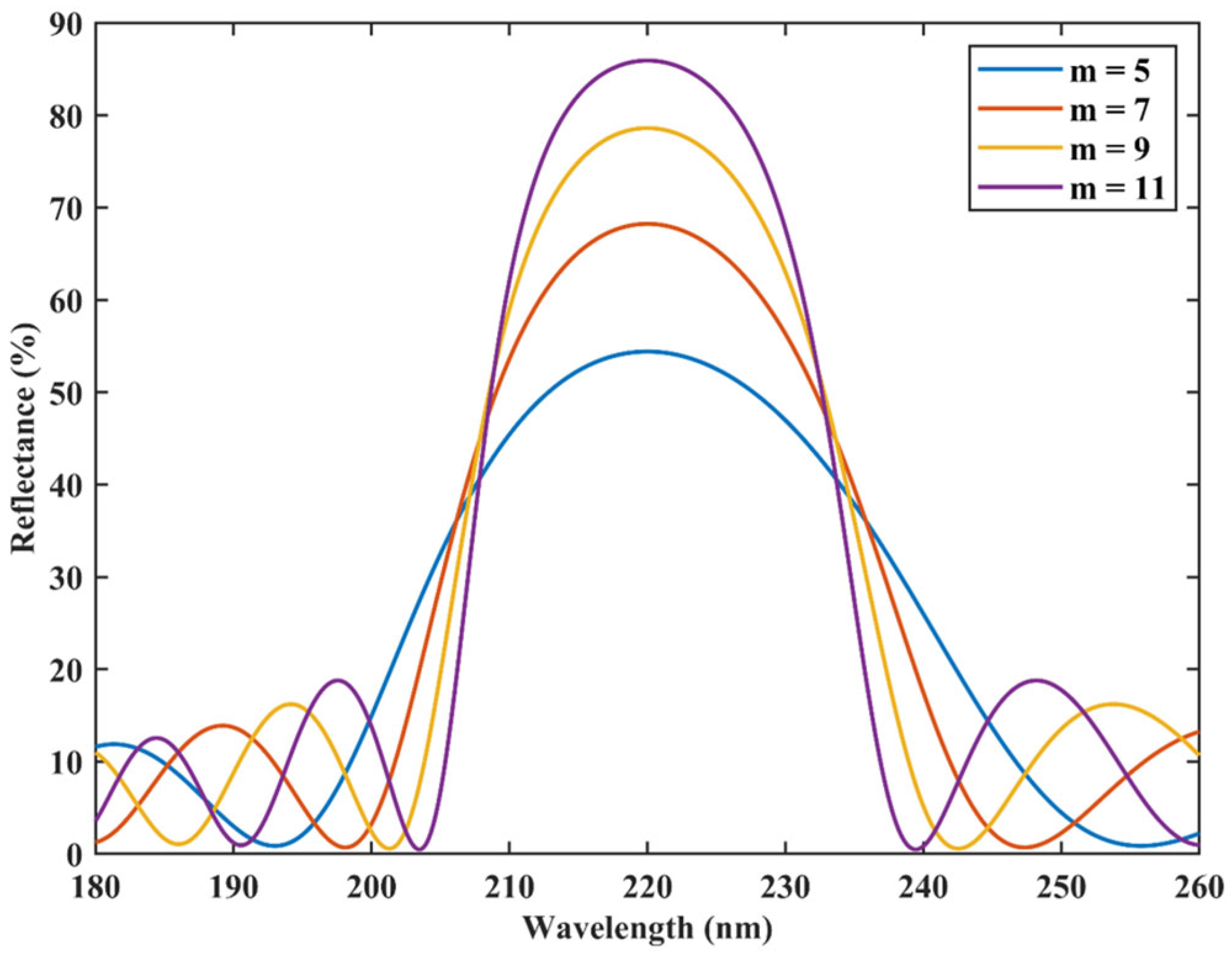
We calculated the reflection spectra under normal incidence over the wavelength range of 180 to 260 nm for four different multilayer structures with alternating period numbers of
m = 5, 7, 9, and 11, using the Transfer Matrix Method. As shown in
Figure 2, the reflectance of the films increases significantly with the number of alternating periods.
Specifically, when m = 5, the reflection peak is relatively broad and smooth, with a reflectance of 54.41%. When m = 7, a secondary peak begins to emerge on the shorter- wavelength side, and the reflectance increases to 68.24%. As m increases further, the secondary peak structure becomes more pronounced, exhibiting multiple distinct periodic sub-peaks. When m = 11, the reflectance reaches 85.93%, with a full width at half maximum of 25.45 nm.
In addition to normal incidence, oblique incidence should also be considered.
Figure 3 shows the variation in reflectance at different incident angles for
m = 11. At an incident angle of 10°, the reflection spectrum exhibits only a slight shift compared to normal incidence. The central wavelength of the main peak remains close to 220 nm, with a slight shift toward the shorter wavelength region. As the incident angle increases to 30°, the main peak shifts further toward shorter wavelengths, and the peak reflectance exhibits a slight decreasing trend. This phenomenon can be attributed to the decrease in the effective optical path length within the multilayer films as the incident angle increases, causing a blue shift of the central wavelength. Additionally, the reflectance coefficients of the polarized components at the interfaces between high- and low-refractive-index materials vary with incident angle, leading to a moderate reduction in overall reflectance. When the incident angle increases to 50°, noticeable changes occur in the spectral profile. The main reflection peak shifts to around 200 nm, while a pronounced minimum appears near 220 nm. At an incident angle of 70°, the reflection spectrum shows further redistribution of peaks and valleys. The main peak shifts toward 190 nm, with the peak reflectance reduced to 70%, and a secondary minimum appears near 220 nm. This indicates that at large incident angles, the phase-matching conditions within the multilayer stack are significantly restructured for different wavelengths. Consequently, the primary high-reflectance band formed under normal or small-angle incidence may become redistributed into multiple secondary interference peaks, thereby reducing reflectance at the design wavelength. In general, the reflective behavior of the multilayer structure exhibits angular dependence. As the incident angle increases, the reflection peak shifts toward shorter wavelengths, accompanied by a noticeable reduction in peak reflectance.
In practice, the angle of incidence on the film surface varies depending on the positions of the point light sources. Therefore, considering only normal incidence or a single oblique angle is insufficient to characterize the real optical behavior. It is necessary to evaluate the overall reflective performance of the multilayer system and further investigate its response to radiation from the light source.
3.2. Analysis of the Influence of Groove Width
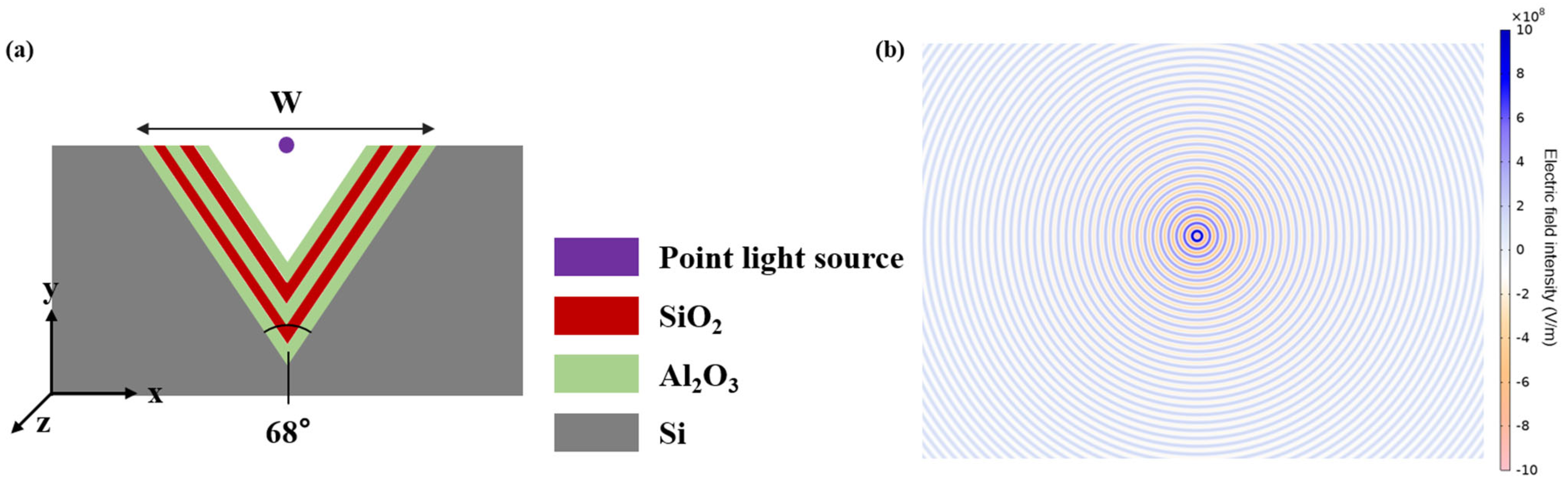
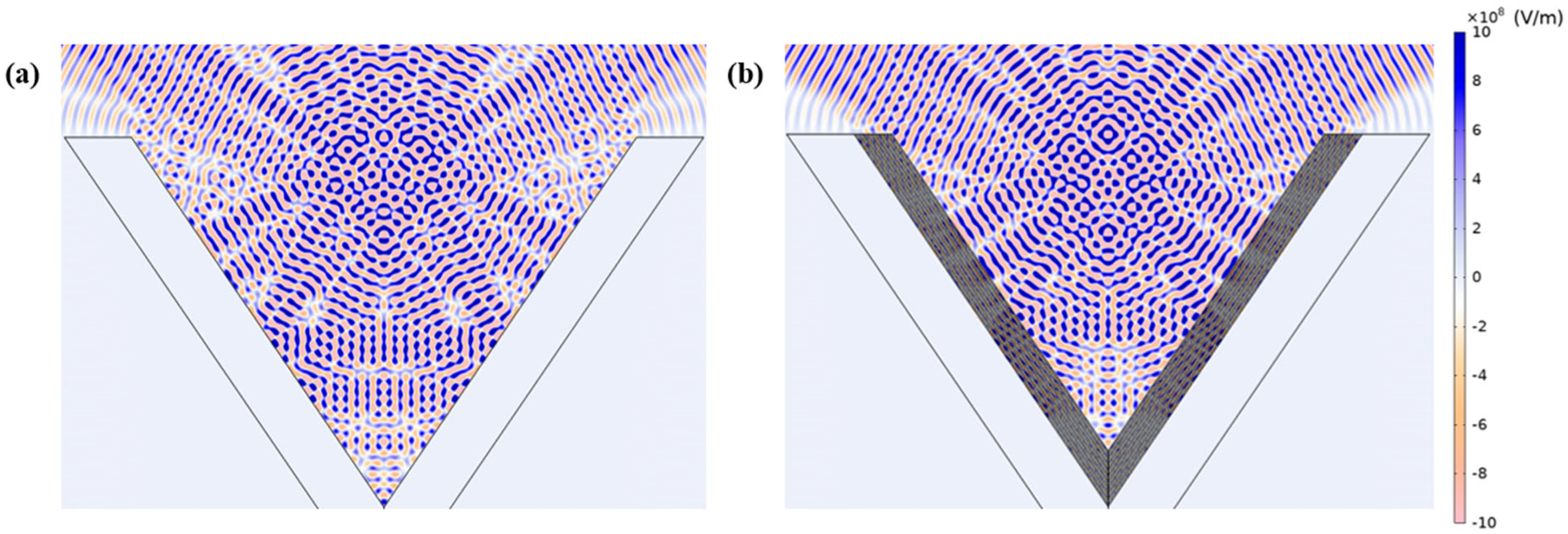
We use a frequency-domain electromagnetic wave analysis tool, which was built in- house based on the finite element method to obtain the electric field distribution and far-field radiation patterns. We conduct simulations at a wavelength of 220 nm, using the corresponding refractive indices for all materials at 220 nm and applying perfectly matched layers [
34] at the boundaries of our computation window. A triangular mesh is applied, with a minimum element size of 15 nm near interfaces and grooves. The near-field electromagnetic response of the device is first computed, and the far-field radiation pattern is then obtained using a far-field transformation. Each V-grooved discharge unit has a depth of about 50 μm [
35] perpendicular to the x–y plane as in
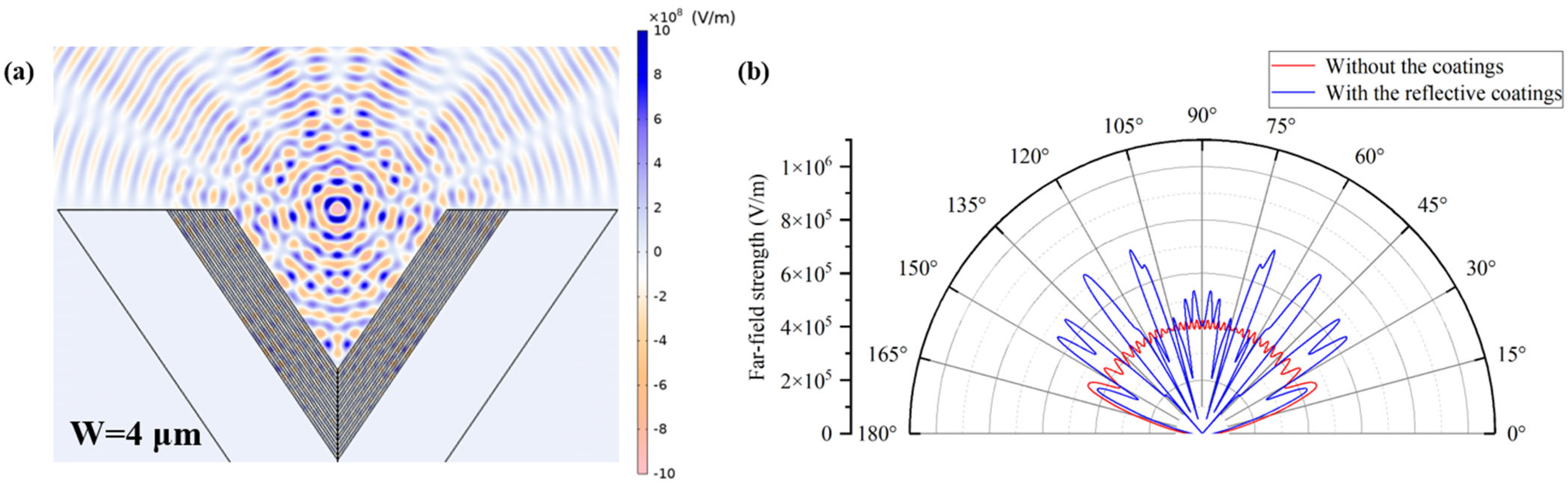
Figure 1a, which is >200 times the wavelength in vacuum, i.e., 220 nm, making field variation along z-direction negligible. Thus, the electro-magnetic responses of the proposed device in the z-dimension can be viewed as effectively uniform. To examine the influence of the structural dimensions of the V-shaped groove on reflective performance, we first consider a case with a groove width,
W, of 10 μm as an example. The resulting electric field distribution and far-field radiation pattern are shown in
Figure 4.
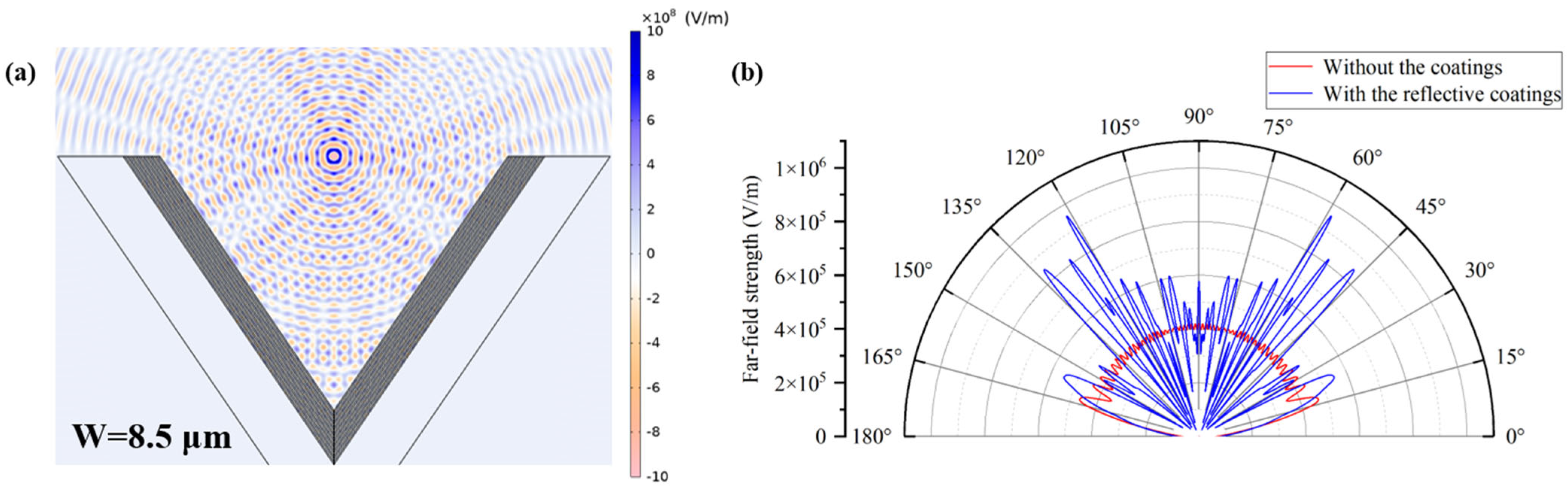
Figure 4a shows the electric field distribution. Compared to
Figure 1b, multiple reflections of electromagnetic waves occur within the V-shaped groove, resulting in the formation of complex standing waves and interference fringes, which indicate local field enhancement. Due to the refractive index contrast between the high- and low-index layers of the multilayer structure, the incident electromagnetic wave undergoes successive partial reflections and transmissions at each interface. These processes cause effective interference between the reflected and transmitted waves within the microscale groove, thereby forming a stable standing wave field distribution.
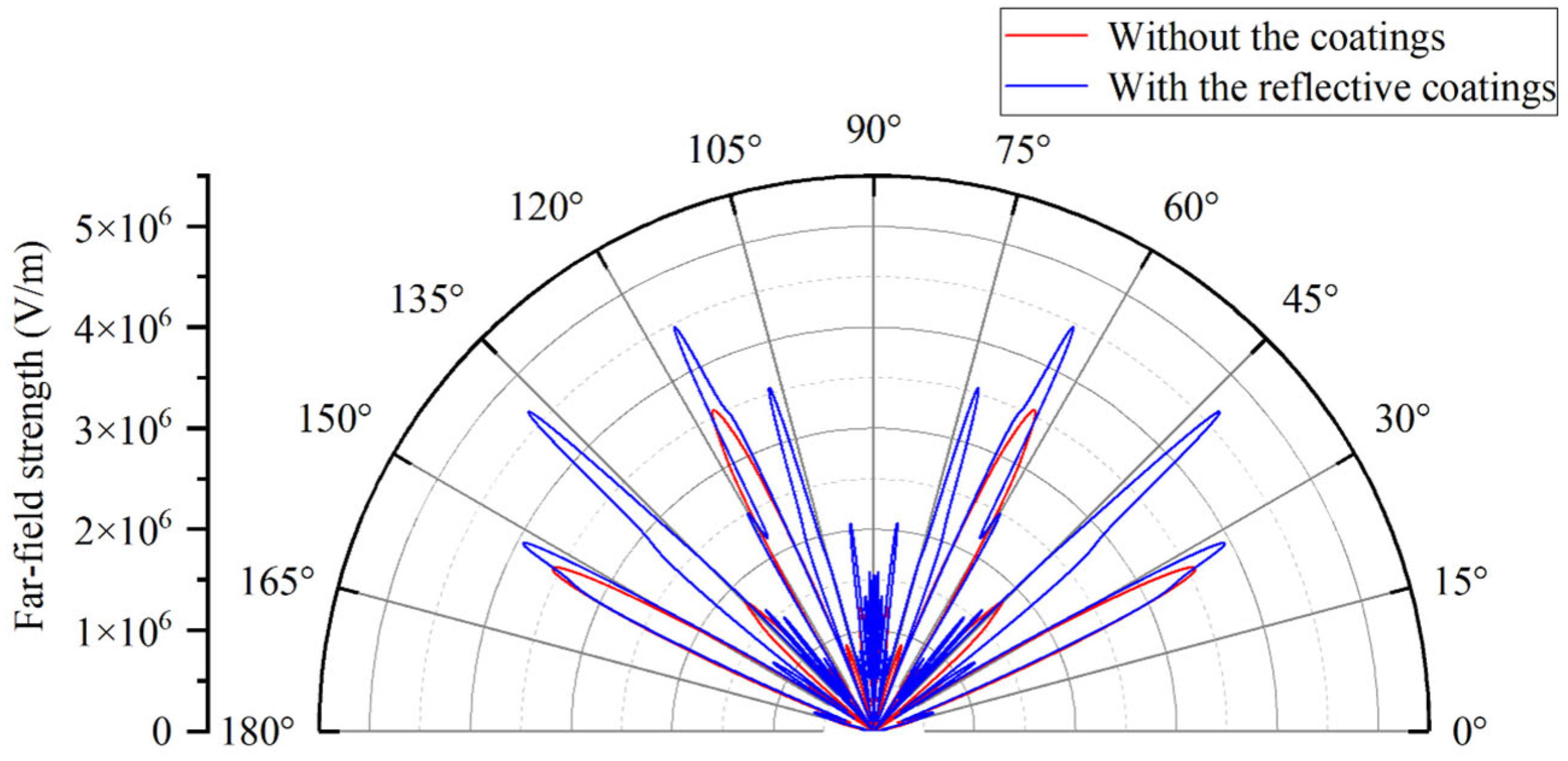
Figure 4b shows the far-field radiation pattern. In the case without the coatings, it exhibits a hemispherical distribution with uniformly distributed energy. In contrast, the presence of several sharp lobes in the case with the reflective coatings suggests that multilayer reflections within the groove lead to a complex far-field radiation pattern. Moreover, the magnitude of the far-field mode shows that the lobe intensity in the case with reflective coatings, which spans angular ranges of approximately 60–75° and 105–120°, is nearly twice that of the case without the coatings, further confirming that multiple reflections within the groove cause constructive interference and upward enhancement.
To quantitatively evaluate the reflective performance of the groove, we further introduce reflection efficiency and power enhancement. These are inspired by prior studies that report relative metrics such as luminescence intensity and conversion efficiency [
23]. By integrating the far-field radiation patterns corresponding to the case without the coatings and the case with reflective coatings, capturing all upward-emitted components, the associated radiated powers emitted above the groove are obtained and denoted as
P1 and
P2, respectively. These quantities correspond to the output optical power above the device. The reflection efficiency can be defined as follows:
This ratio represents the proportional contribution of the reflective structure to the far-field radiation and reflects its effective utilization in the total radiated energy. It serves as a useful metric for evaluating the effectiveness of the proposed device in terms of reducing losses and improving energy utilization. The power enhancement can be defined as follows:
This ratio represents the percentage increase in radiation for the case with reflective coatings relative to the case without coatings, indicating the effectiveness of the groove-shaped multilayer device in enhancing overall radiation. It can be used to evaluate the ratio of the increased radiated power to the original radiated power.
The far-field radiation data are integrated, yielding the radiated powers P
1 and P
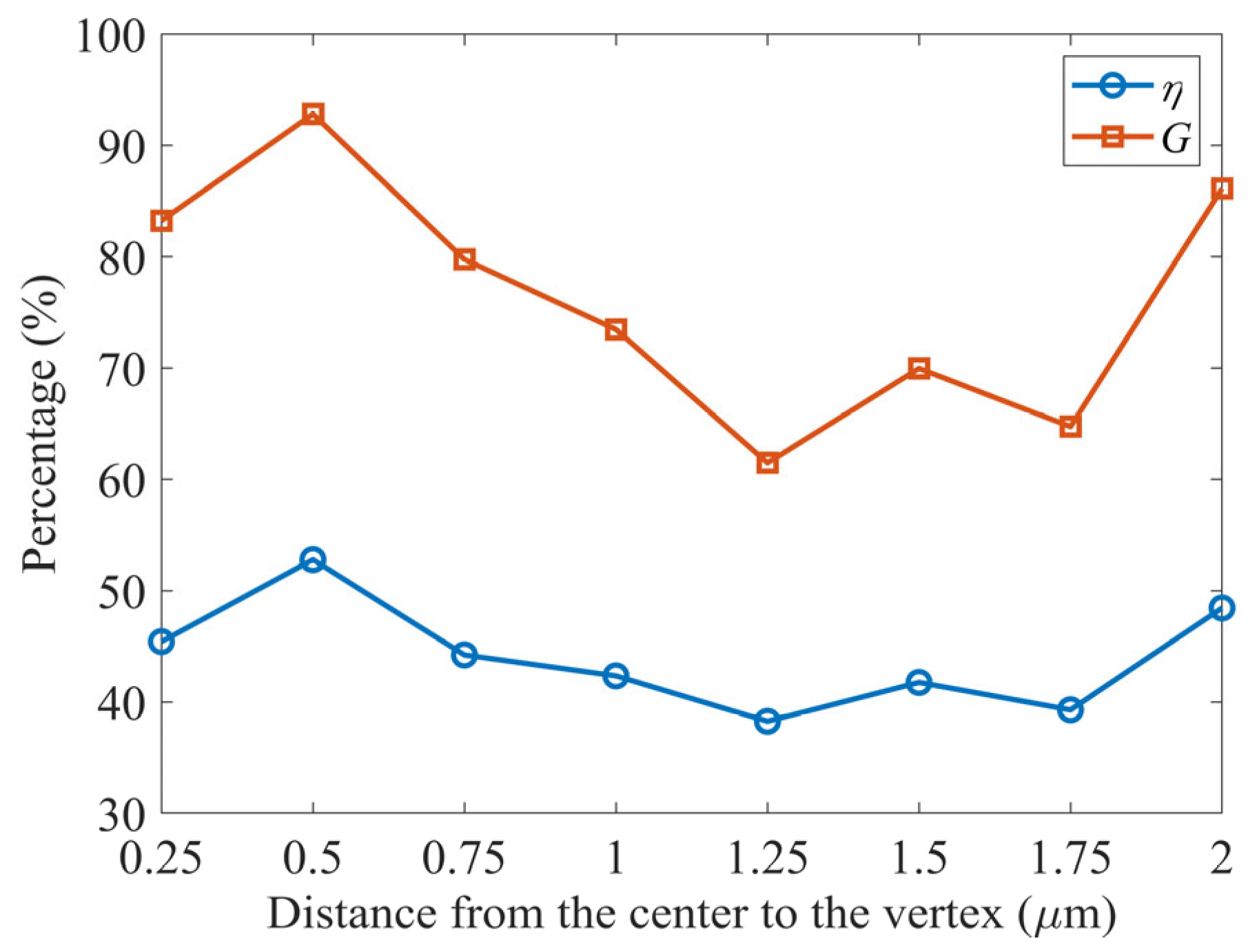
2 for the cases without and with reflective coatings, respectively. By substituting these values into Equations (1) and (2), the reflection efficiency and power enhancement for W = 10 μm are calculated to be 42.87% and 75.03%, respectively. They are calculated for different groove widths, as shown in
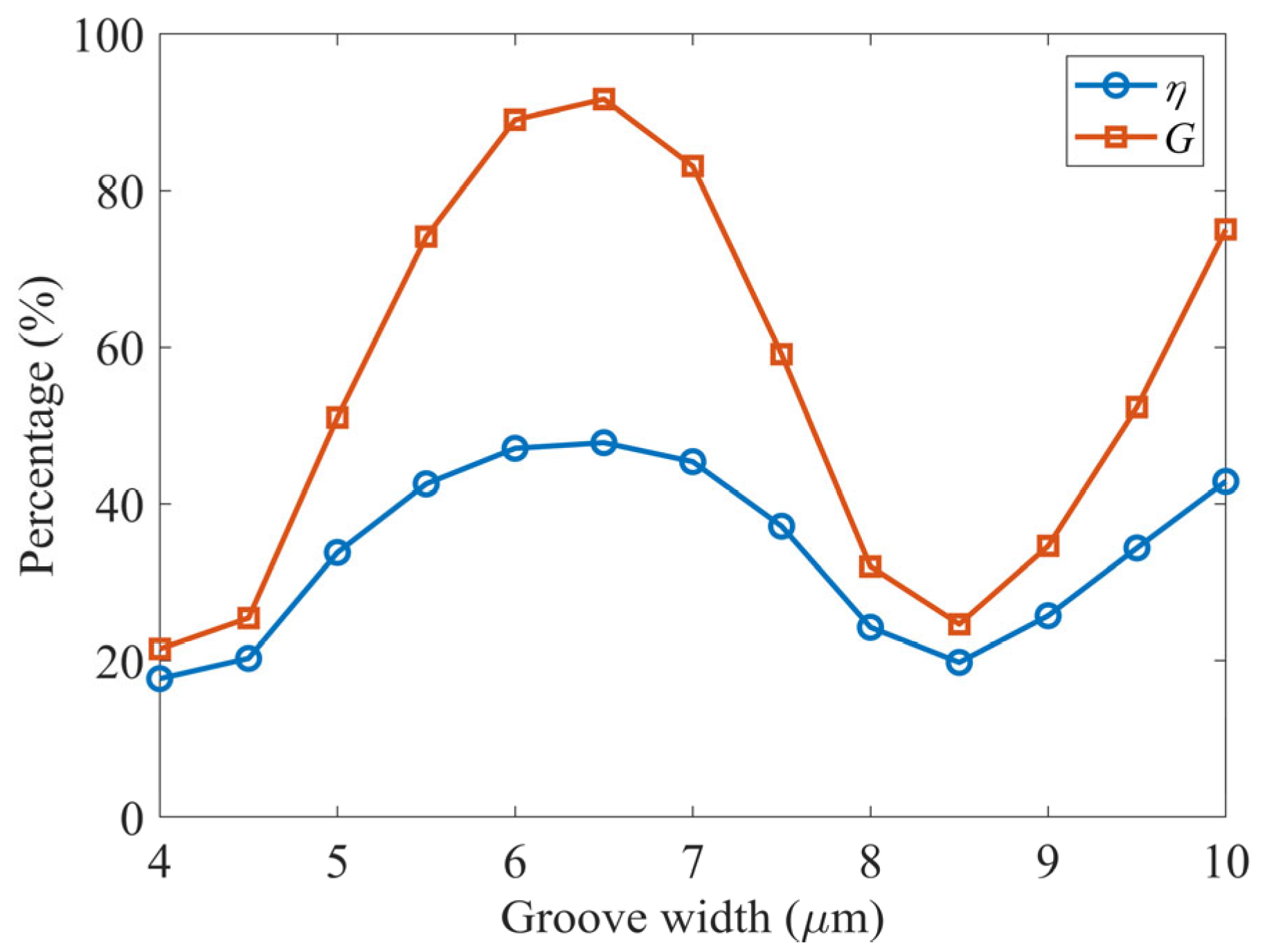
Figure 5.
When the groove width is reduced from 10 μm to 8.5 μm, the reflection efficiency decreases to 19.77%, and the power enhancement drops to 24.64%. The corresponding electric field intensity and far-field radiation pattern are shown in
Figure 6. As shown in
Figure 6a, the multilayer film within the groove continues to change the electric field. However, the interference fringes are significantly less distinct and concentrated compared to the case with
W = 10 μm. The electromagnetic waves exhibit increased divergence near the groove opening. Along the reflection path, destructive interference becomes more pronounced, indicating that the optical path differences at multiple positions no longer correspond to integer multiples of the wavelength, thereby suppressing constructive interference. Meanwhile,
Figure 6b shows that both the amplitudes and the number of lobes are greatly reduced. The radiation intensity in multiple directions is noticeably weakened, showing that the conditions for multipath interference are no longer satisfied in this case, leading to dispersion and attenuation of the radiated energy.
When the groove width is further reduced from 8.5 μm to 6.5 μm, the device exhibits optimal reflective performance, with reflection efficiency and power enhancement reaching peak values of approximately 47.82% and 91.66%, respectively. The corresponding electric field intensity and far-field radiation pattern are shown in
Figure 7. As shown in
Figure 7a, distinct and intense interference fringes are formed within the V-shaped groove, exhibiting strong constructive interference. The electric field is highly concentrated around the groove opening, exhibiting a high-density distribution. The wavefront displays good symmetry and radiates outward in the vertical direction, showing that the energy undergoes multiple reflections within the cavity and is effectively coupled and emitted in a stable direction.
As shown in
Figure 7b, the number of lobes increases, and the radiation intensity is significantly enhanced in multiple directions compared to
Figure 4b. This phenomenon can be attributed to the enhanced phase accumulation effect resulting from multiple reflections within the cavity, which leads to more pronounced interference superposition. As a result, stronger upward radiation characteristics and a more concentrated energy distribution are observed in the far field. Furthermore, the enhancement of lobes also shows that local coherent superposition is simultaneously achieved along multiple interference paths, further improving overall radiation efficiency. Consequently, a groove width of
W = 6.5 μm can be considered the optimal design parameter, as it effectively enhances both reflection efficiency and energy output.
As the groove width is further reduced to 4 μm, the reflective performance deteriorates significantly. The reflection efficiency decreases to 17.69%, and the power enhancement drops to 21.49%. The corresponding electric field intensity distribution is shown in
Figure 8. The interference fringes in the V-shaped groove region appear sparse, with an overall reduction in field strength. Although some reflection still occurs within the groove, the reflected wavefronts fail to achieve phase matching, preventing significant coherent superposition. As a result, the energy reutilization efficiency within the structure is substantially reduced. This result indicates that when the groove becomes too narrow, the propagation and reflection paths of the light waves are severely constrained, ultimately leading to a substantial reduction in the structure’s ability to release reflected energy. This manifests as a degradation in reflective performance.
As shown in
Figure 8b, although the intensity is slightly enhanced compared to the case without the coatings, the overall radiation remains weak. The far-field energy distribution exhibits a low-intensity diffusion pattern. This radiation pattern shows that under these conditions, the reflected energy within the groove cavity cannot be effectively directed outward. These characteristics indicate that when the groove width is reduced below a certain threshold, the device can no longer establish an effective upward cavity-reflection mechanism. Even though multiple reflections may still occur, the lack of constructive interference leads to dispersed energy distribution. Ultimately causing low far-field output, limited reflection efficiency, and minimal power enhancement.
Therefore, by appropriately tuning the geometric dimensions of the groove, the internal reflection paths, phase accumulation mechanisms, and interference effects of electromagnetic waves can be effectively controlled, resulting in a notable enhancement in the device’s reflective performance.
3.3. Analysis of the Influence of Light Source Position
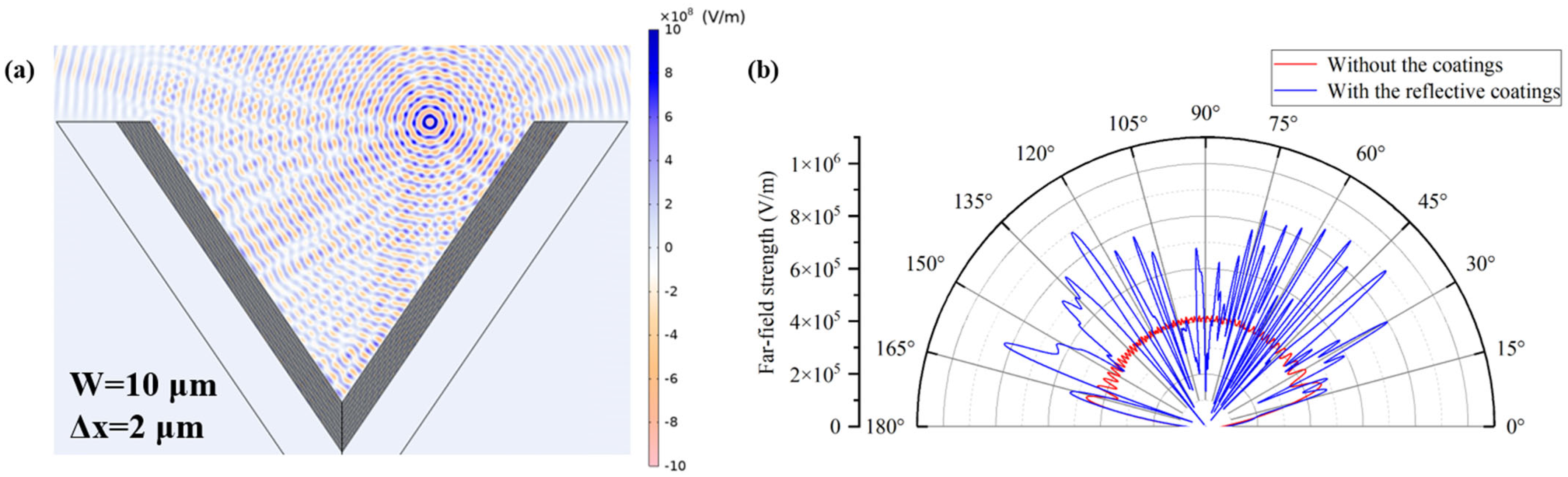
Under practical experimental conditions, the ultraviolet light source generated via microplasma is often not precisely aligned with the geometric center of the groove-shaped device due to inherent limitations in alignment accuracy. Therefore, we further investigate the effects of source offset relative to the center of the groove structure. The results obtained with a groove width of
W = 10 μm and the light source positioned at the geometric center of the device serve as the reference.
Figure 9 shows the electric field intensity and far-field radiation pattern resulting from a 1 μm offset of the light source along the
x-axis, with the groove width and other structural parameters at constant.
When the light source is displaced along the
x-axis, the wavefronts incident on the left and right walls of the groove experience unequal optical path lengths, leading to an initial phase difference. As shown in
Figure 9a, the interference fringes on the right side of the groove become denser with significantly enhanced local field intensity, whereas those on the left side appear sparser with reduced field strength. This asymmetric field enhancement primarily arises from the accumulated phase difference caused by variations in propagation path lengths when the light source is displaced from the central position, resulting in uneven coherent superposition of the reflected waves within the groove.
The corresponding far-field radiation pattern is shown in
Figure 9b. It can be observed that the radiation direction no longer exhibits the original symmetrical distribution. The asymmetry in the lobe distribution arises from the optical path difference between the two groove walls. The offset causes shorter optical paths for reflection on the nearer side, resulting in denser and more intense lobes concentrated in 45–75°. Conversely, reflection from the farther side experiences longer paths, leading to sparser lobes distributed between 105 and 135°. This phenomenon shows the complex radiation characteristics resulting from the combined effects of propagation path length differences and interference at the multilayer interfaces under source offset conditions.
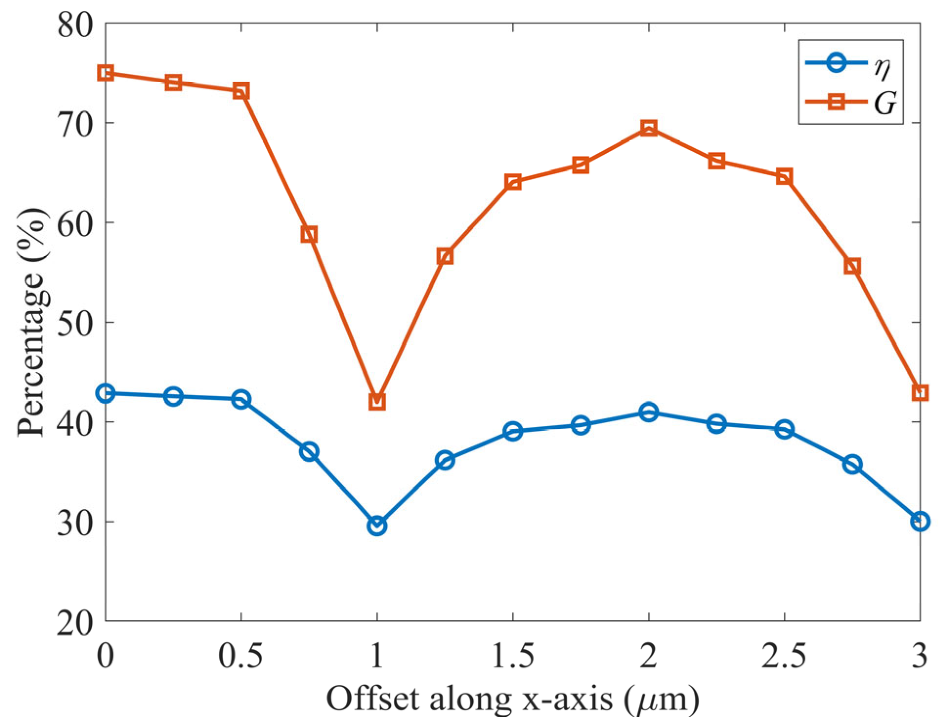
The reflection efficiency and power enhancement at different offset values of the light source along the
x-axis are calculated, as shown in
Figure 10.
It is observed that as the light source offset increases, the reflection efficiency slightly decreases, reaching a minimum of 29.57% at an offset of 1 μm. Simultaneously, the power enhancement drops significantly to 41.99%, indicating that the structural symmetry is disrupted at this offset, leading to phase interference along the reflected light paths and subsequently reducing the far-field energy output.
When the offset is further increased to 2 μm, both metrics show partial recovery, with the reflection efficiency rising to 40.99% and the power enhancement reaching 69.47%. However, neither returns to the initial values. The corresponding electric field intensity and far-field radiation pattern are shown in
Figure 11. The interference fringes of the electric field become increasingly asymmetric, with reflection paths enhanced on the side closer to the offset and weakened on the opposite side. As shown in
Figure 11b, the number of lobes increases significantly on the side closer to the offset, accompanied by enhanced radiation intensity in multiple directions. This may be attributed to changes in the incident angle of light at fixed positions on the multilayer surface as the offset increases, causing improved reflective performance compared to the case with a 1 μm offset.
However, as the offset continues to increase, the reflective performance drops sharply once again, indicating that the effective reflective region of the structure is spatially bounded. Beyond this range, the radiated energy can no longer be efficiently controlled. This result shows that the groove exhibits high sensitivity to the light source position, and its alignment accuracy directly affects the performance of the reflected radiation.
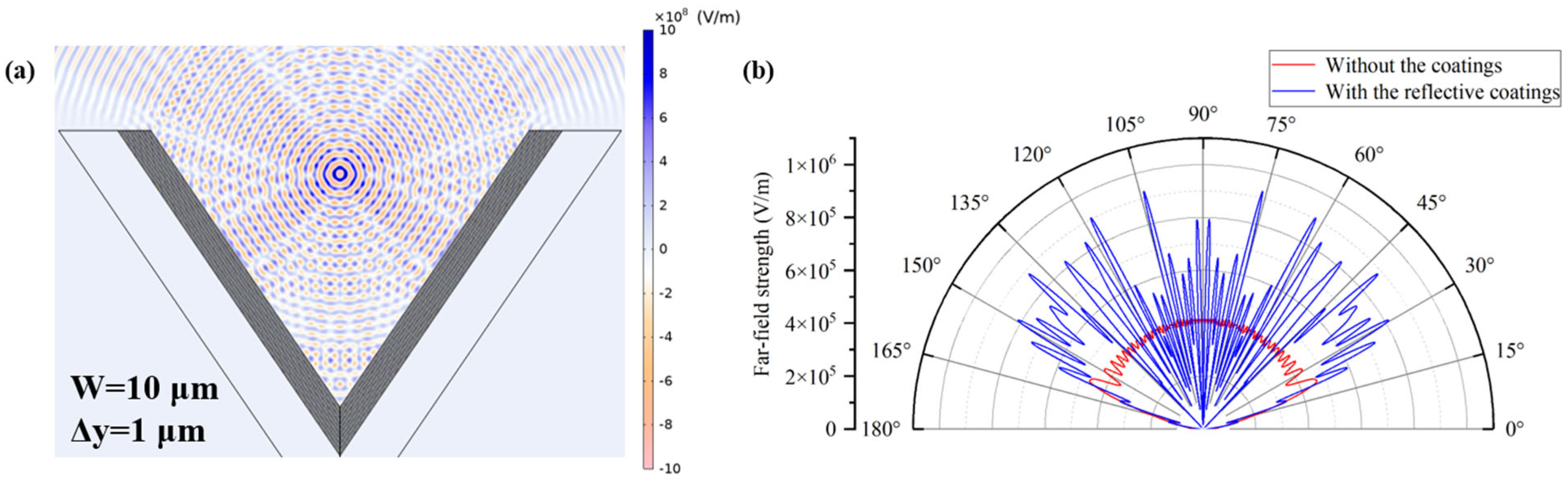
In addition to the
x-axis offsets, we also perform simulations and analyses for light source offsets along the
y-axis. When the light source is offset by 1 μm along the
y-axis, the electric field intensity and far-field radiation pattern are shown in
Figure 12. The light source is positioned closer to the bottom region of the groove, significantly shortening the propagation distance of the initial incident wavefront to the sidewalls and thereby reducing the internal reflection path length of the electromagnetic waves. This change in the propagation path directly causes an overall upward shift of the interference fringes inside the groove, which signifies more energy being funneled toward the groove opening. The regions of enhanced field intensity move noticeably toward the groove opening, and a strong interference-enhanced band appears near the opening region.
Meanwhile, as shown in
Figure 12b, when the light source is offset along the
y-axis, the lobe intensity in the far-field radiation shows no significant change compared to the case where the light source is positioned at the geometric center of the groove. However, it is noteworthy that the number of lobes along the 90° direction increases significantly, accompanied by a denser spacing between lobes. This variation in lobe distribution shows that the downward offset of the light source shortens the initial reflection paths between the groove walls, thereby enhancing the coherent superposition of electromagnetic waves near the groove opening. Consequently, the radiation becomes more strongly concentrated in the direction perpendicular to the groove opening, leading to a more pronounced upward radiation pattern. The reflection efficiency at this offset is calculated to be 42.34%, with a corresponding power enhancement of 73.43%. This result indicates that the device’s reflective performance undergoes only a slight reduction and remains within an acceptable range.
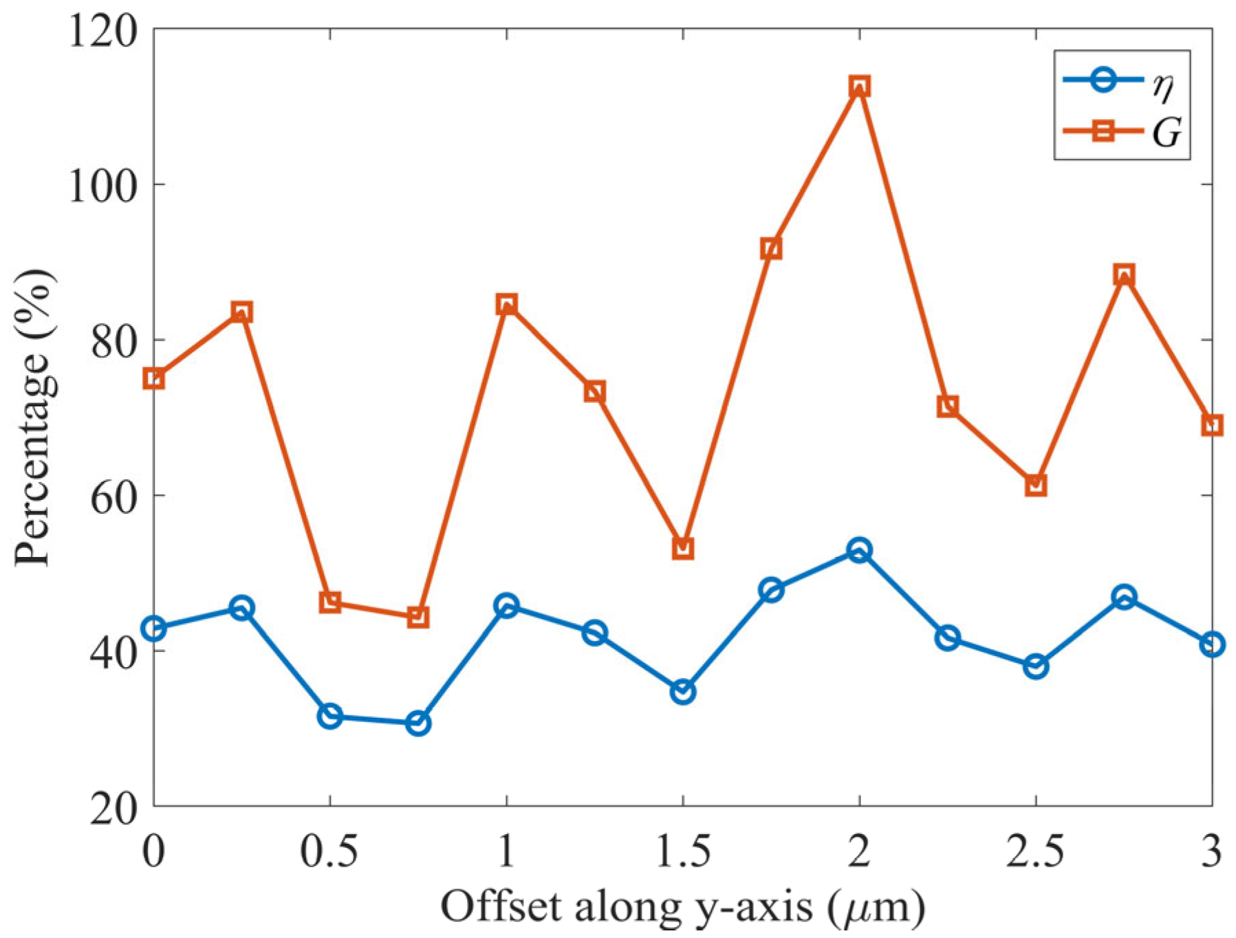
Figure 13 shows the variations in reflection efficiency and power enhancement under different
y-axis offsets of the light source. It is observed that the structure exhibits a periodic response during the y-direction offset process, with performance peaks appearing at multiple offset positions. Specifically, when the offset reaches 0.25 μm, the reflective performance is slightly improved compared to the initial position. As the offset increases to 0.5 μm, both the reflection efficiency and power enhancement drop significantly, reaching 31.6% and 46.2%, respectively. At an offset of 1 μm, both metrics rise again, with the reflection efficiency reaching 45.81% and the power enhancement increasing to 84.55%. As the light source is further offset to 1.5 μm, the performance declines once more. However, at 2 μm, a substantial improvement is observed, with the reflection efficiency and power enhancement reaching 52.96% and 112.59%, respectively, which represent the highest values within the scanned range. Subsequently, a local peak also appears at an offset of 2.75 μm, while at 2.5 μm and 3 μm, the reflective performance exhibits varying degrees of decline.
These results show that the groove exhibits a certain degree of spatial selectivity to offsets along the y-axis. Variations in reflection paths and phase-matching conditions at different offsets jointly determine whether interference enhancement or suppression occurs within the structure. In particular, an offset of 2 μm appears to create more favorable conditions for coherent superposition, thereby enhancing reflective performance and significantly boosting power output.
According to the analysis of
Figure 10 and
Figure 13, the groove is more sensitive to offsets along the
x-axis, while exhibiting a certain degree of spatial selectivity along the
y-axis under the condition of ensuring efficient coupling and reflection of the point source. Nevertheless, regardless of the light source position, the structure consistently maintains relatively good reflective performance within a certain range.
3.4. Analysis of the Influence of Multiple Light Sources
To examine real conditions more accurately, we further investigate the electromagnetic response of the coatings in a 10 μm-wide groove by arranging multiple point sources. Specifically, nine point sources are placed in a tilted square array, positioned at the center, the four corners, and the midpoints of the four sides of the square.
Figure 14 shows the corresponding electric field distributions. Without the coatings, the multiple point sources generate interference fringes, while about 34% of UV light is absorbed by the silicon substrate. In contrast, with the reflective coatings, we see enhanced standing wave patterns both inside and above the groove. Notably, previously downward UV light undergoes multiple internal reflections and is redirected upward.
The corresponding far-field radiation patterns are shown in
Figure 15. Compared to the case without coatings, significantly enhanced upward radiation is found. In particular, the intensities at 45° and 135° increase by nearly threefold. This shows that the groove facilitates constructive interference within specific angular ranges, thereby enhancing upward radiation. Further calculations reveal that the reflection efficiency and power enhancement of this configuration increase to 42.35% and 73.41%, respectively. These results further confirm the effectiveness of the V-grooved reflective coatings in enhancing UV light extraction, suppressing backward losses, and improving the overall utilization efficiency of the emitted light.
We evaluated the reflective performance of the device under varying spacing between point sources, as shown in
Figure 16. The results show that even in the lowest-performing configuration, the reflection efficiency remains close to 40%, and the power enhancement exceeds 60%. This indicates that the proposed structure exhibits stable reflective performance under different point source arrangements, effectively enhancing ultraviolet emission across a range of excitation conditions.
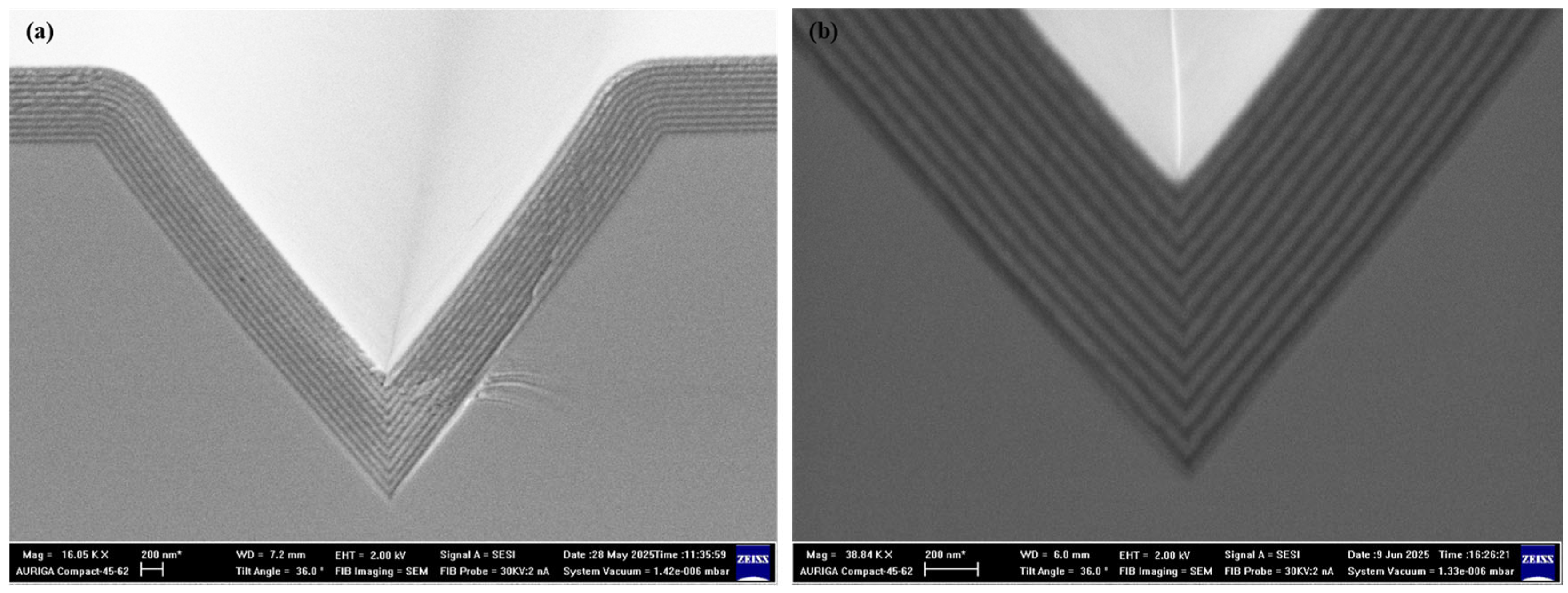
We fabricate the V-shaped grooves and deposit the multilayer reflective coatings. From
Figure 17, one can see that the proposed device is successfully fabricated with highly uniform and conformal coatings formed. In practical implementations, arrays containing hundreds or thousands of such grooves will be fabricated on a chip, providing cumulative UV output sufficient for applications such as disinfection and sensing. However, due to the lack of some necessary equipment, ultraviolet microplasma excitation cannot be conducted at this stage. When operated in microplasma mode, the coatings may have performance degradation due to possible heating, sputtering, transformation, and contamination.

