1. Introduction
In 1916, Einstein formulated the theoretical framework of general relativity and first predicted the existence of gravitational waves. Nearly a century later, in 2015, the ground-based gravitational wave detector LIGO made the first direct detection of these waves [
1,
2], marking the beginning of gravitational wave astronomy. Due to the influence of Earth’s gravitational field variations, surface vibrations, and other environmental factors, ground-based detectors are primarily sensitive to frequencies above 10 Hz. To observe gravitational wave sources with greater mass, at larger distances, and in lower-frequency bands, it is essential to overcome the limitations inherent in ground-based detection [
3]. Deploying space-based detectors with very long baselines presents the most promising solution. These detectors utilize the principle of laser heterodyne interferometry to measure the relative displacement between spacecraft by detecting the phase shift in the interference signal. The payload responsible for measuring this phase shift is referred to as a phasemeter. According to system-level performance requirements, the phasemeter must achieve a displacement sensitivity of 1 pm, corresponding to a phase measurement noise requirement of 2π μrad/Hz
1/2@(0.1 mHz–1 Hz) in the frequency range of 0.1 mHz to 1 Hz. Current major space-based gravitational wave detection initiatives include LISA [
4,
5], the Taiji program [
6,
7], and the Tianqin program [
8,
9].
The interference signal is first rectified and filtered by a QPD and then digitized by an ADC, which converts the continuous-time, continuous-amplitude beat signal into a sequence of discrete digital values. Digitization is inherently a nonlinear process, as it involves rounding the analog signal to the nearest quantized level. The primary noise sources in the analog-to-digital conversion process are quantization noise and sampling timing jitter. Since the linear spectral density of phase noise induced by quantization is typically negligible, sampling clock jitter becomes the dominant source of phase noise in the digitization of beat frequency signals [
10]. To mitigate this effect, noise suppression techniques are employed to compensate for ADC sampling delay mismatches across QPD detector channels, thereby improving the accuracy of phase measurement.
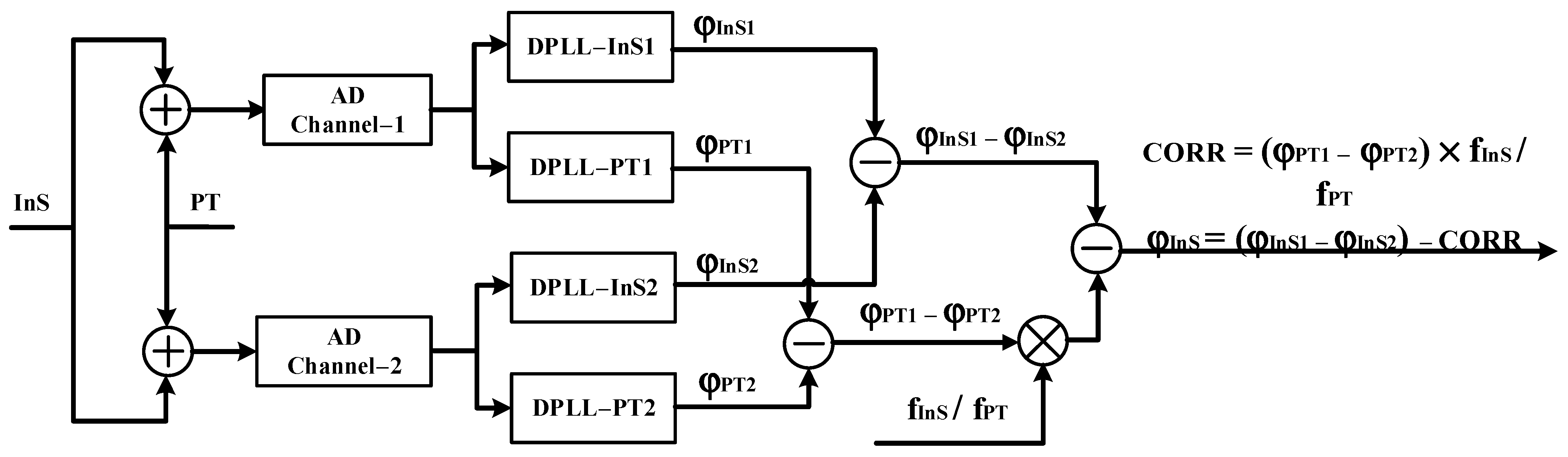
Currently, the major space-based gravitational wave detection programs employ a method based on pilot tone calibration for ADC sampling timing jitter correction [
11,
12,
13]. This is achieved by injecting a stable reference pilot tone signal with a fixed frequency into the input of each ADC. The phase noise obtained from the phase measurement of the high-frequency pilot tone signal is primarily attributed to ADC sampling timing jitter. Adding a pilot tone signal to all ADC channels allows the phase jitter component of the beat signal’s phase measurement to be effectively eliminated through the phase measurement results from the pilot tone signal. Clock stability plays a critical role in the performance of phase measurement, making it essential to use an ultra-stable clock as the system clock for the phasemeter. To eliminate the phase noise from the oscillator generating the pilot tone and the phase jitter between interstellar pilot tones, the high-frequency signal, after frequency doubling of the pilot tone, is phase-modulated onto the laser link carrier [
14]. This enables the transfer of interstellar clock noise, thereby facilitating subsequent data post-processing.
Barke [
14] designed an interstellar frequency allocation system for the LISA mission according to its requirements. For the frequency range of 7 to 23 MHz of the heterodyne interference signals, the ADC sampling frequency was set to 80 MHz and the pilot tone frequency was set to 75 MHz. Kullmann [
15] configured the ADC sampling frequency to 50 MHz and the pilot tone frequency to 72 MHz for the frequency range of 2 to 20 MHz of the heterodyne interference signals. Liang [
13] proposed a method of adding a pilot tone to the measurement signal, with an ADC sampling frequency of 50 MHz and a pilot tone frequency of 24.3 MHz. Liu [
16] conducted a phase noise test on a 14 MHz heterodyne interference signal, with an ADC sampling frequency of 80 MHz and a pilot tone frequency of 14 MHz. Huang [
17] performed phase noise testing on a 15 MHz heterodyne interference signal, with a pilot tone frequency of 31 MHz. Zhang [
18] tested phase noise for heterodyne interference signals at 5 MHz, 10 MHz, 15 MHz, 20 MHz, and 25 MHz, using an ADC sampling frequency of 80 MHz. The pilot tone frequencies used were 15.1 MHz, 25.1 MHz, 25.1 MHz, 25.1 MHz, and 29.1 MHz, respectively.
At present, many research teams conduct experiments on sampling timing jitter noise suppression by simulating pilot tones using signal generators. However, the high-frequency signal used for inter-satellite clock noise transfer, the system clock, and the pilot tone are indispensable components of the phasemeter. Therefore, it is essential to develop a dedicated sampling timing jitter noise suppression System (STJNSS). This system must also accommodate the diverse frequency requirements of future engineering applications. In this paper, we propose a comprehensive design of the STJNSS. It allows parameter adjustment of the high-frequency signal for inter-satellite clock noise transfer, the phasemeter’s system clock, and the pilot tone for suppressing ADC sampling timing jitter, in accordance with the requirements of current major space-based gravitational wave detection missions. Based on the authors’ previous research on phasemeters [
19], for heterodyne signals with a dynamic frequency range of 5 to 25 MHz, we set the ADC sampling frequency to 80 MHz and the pilot tone frequency to 31 MHz. Phase measurement noise was better than 2 πμrad/Hz
1/2 in the 0.1 mHz–1 Hz band. We then integrated the STJNSS with the phasemeter and conducted phase noise evaluation experiments. With the pilot tone set to 75 MHz, the system clock at 80 MHz, and the heterodyne signal at 10 MHz, the results demonstrated phase measurement noise better than 2πμrad/Hz
1/2 in the 0.1 mHz–1 Hz band, satisfying space gravitational wave mission requirements. These results verify the feasibility and correctness of the STJNSS design and demonstrate its potential for future engineering deployment. This also marks a significant extension of existing phasemeter research and provides a valuable reference for future phasemeter design and optimization.
2. Design Scheme of STJNSS
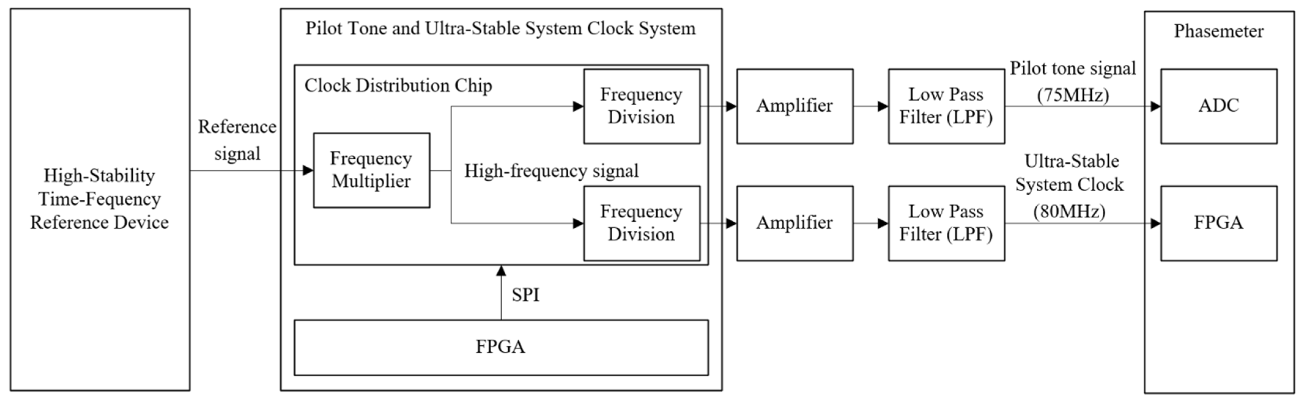
The design architecture of the STJNSS in this scheme is shown in
Figure 1. The ultra-stable system clock and low phase noise pilot tone are important guarantees for the phasemeter to realize micro-radian scale phase measurement [
20], at the same time taking into account the transfer characteristics of the pilot phase noise and clock noise in the interstellar link [
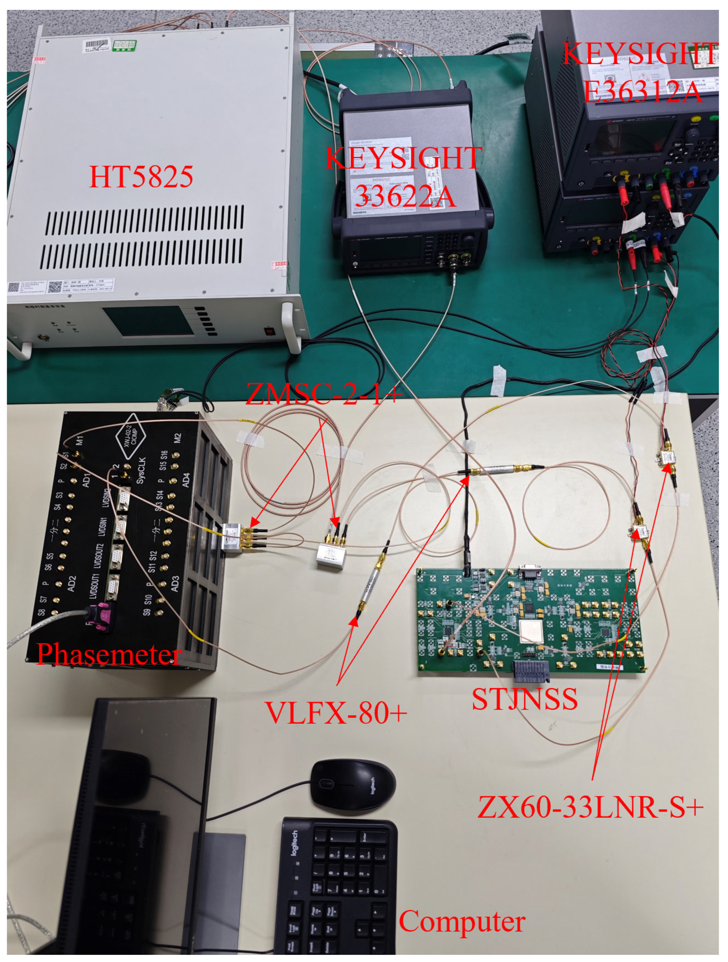
21]. The system adopts the design scheme of frequency doubling followed by frequency division, in which the reference signal from the ultra-stable rubidium clock is doubled by the internal phase-locked loop of the clock distribution chip to generate a high-frequency clock signal, and then transmitted through the tunable frequency divider to obtain the target frequency signal. The field-programmable gate array (FPGA) dynamically configures the multiplication coefficient and division ratio of the chip through the serial peripheral interface (SPI) interface to realize the flexible adjustment of the output frequency. After further processing, the pilot tone and ultra-stable system clock are connected to the phasemeter‘s ADC module and FPGA module, respectively, via an amplifier and low-pass filter. By measuring the phase noise of the heterodyne interferometric signal at the phasemeter output, the design validity and engineering feasibility of the proposed sampling timing jitter noise suppression system are experimentally verified.
In terms of key component selection, the amplifier chosen is Mini-Circuits’ (Brooklyn, NY, USA) ZX60-33LNR-S+, which features a low noise figure across the 50 MHz to 3 GHz range, effectively suppressing link noise and improving the signal dynamic range. The low-pass filter selected is the VLFX-80+ from the same company, with a passband range of DC to 80 MHz, which filters out high-frequency interference and meets the bandwidth requirements of the pilot tone and ultra-stable system clock signals.
2.1. Clock Chip Selection and Peripheral Circuit Design
Texas Instruments (Dallas, TX, USA) LMK04828 is selected as the clock distribution chip for this design. The device integrates dual phase-locked loops (PLLs) and dual voltage-controlled oscillators (VCOs), with VCO operating frequency ranges of 2370–2630 MHz and 2920–3080 MHz, covering the GHz frequency range required for the design’s high-frequency clock. The chip supports 14 signal outputs, each with an independent frequency division ratio (1–32), allowing flexible adaptation to various pilot tone signals and ultra-stable system clock output requirements. Additionally, the chip’s built-in system reference clock module supports independent frequency division control, with a division range of 8–8191, enabling the high-frequency clock signals from the VCO to be divided as low as 3 kHz, extending the test signal frequency into the low-frequency range. In terms of signal integrity, the LMK04828 exhibits excellent phase noise performance. For example, at an output frequency of 245.76 MHz and within a measurement bandwidth of 12 kHz to 20 MHz, its phase jitter is only 88 fs RMS. Considering its wide frequency coverage, flexible output configuration, and low-noise characteristics, the LMK04828 is an ideal choice for the clock distribution module in this system.
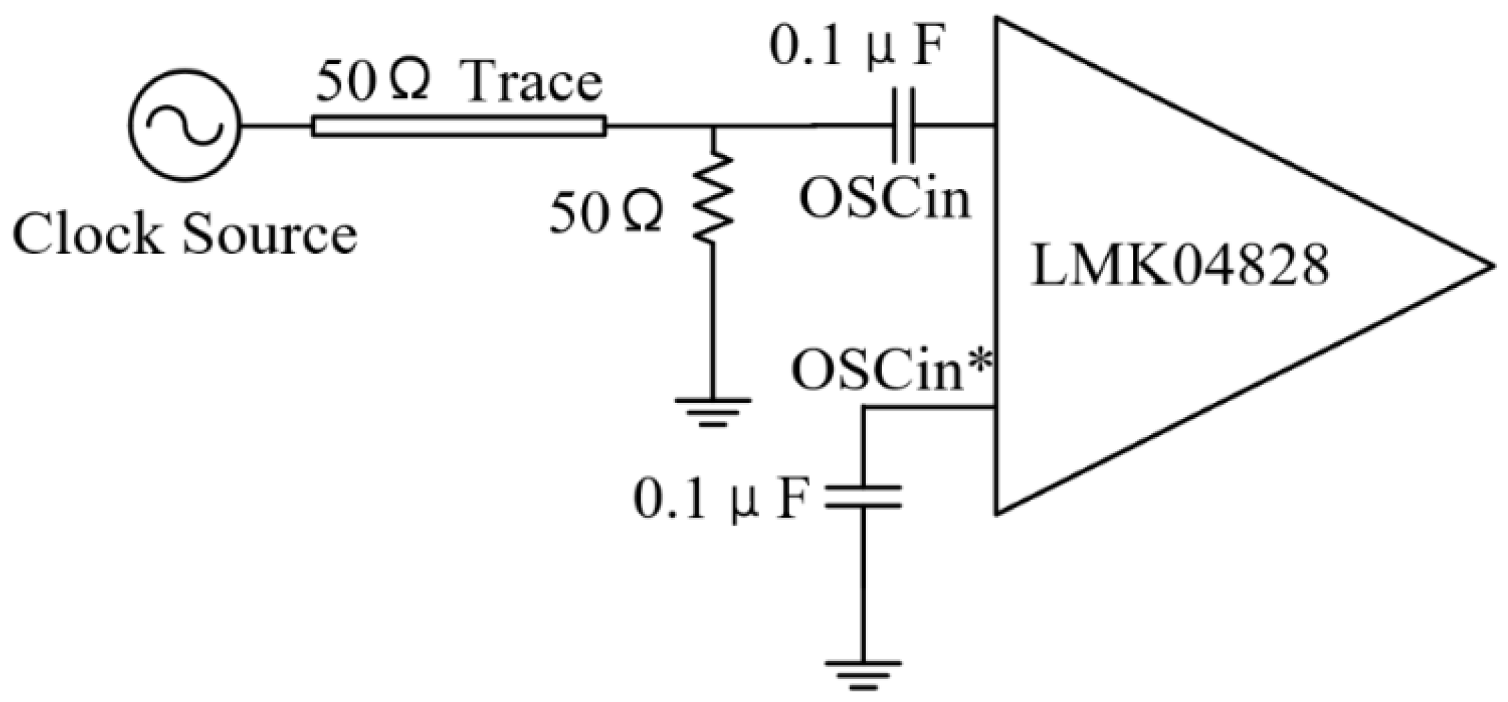
In the reference clock input design, the reference signal for the LMK04828 is provided by an ultra-stable rubidium clock, with the two connected via AC coupling (as shown in
Figure 2), and a 0.1 μF isolation capacitor is connected in series in the signal link to achieve DC bias isolation.
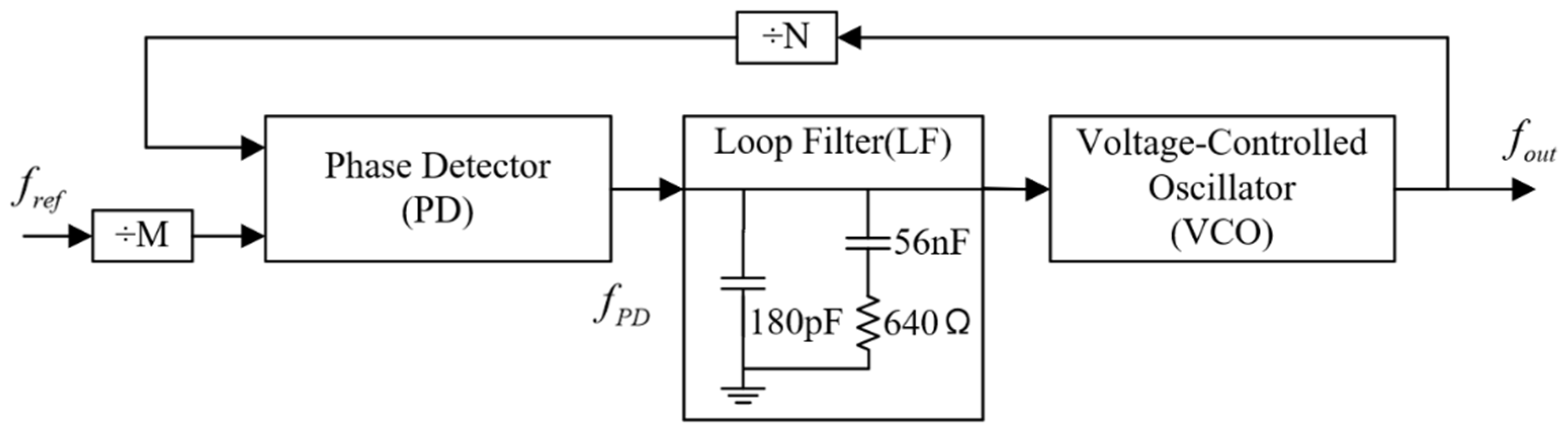
In this design, the core architecture of the phase-locked loop (PLL) consists of a phase discriminator (PD), a loop filter (LF), and a VCO (shown in
Figure 3). To meet the application requirements of the LMK04828 chip, a dedicated LF needs to be designed for the peripheral circuitry. The core function of the filter is to filter out the high-frequency noise and error components in the PD’s output signal while retaining the low-frequency control voltage to accurately regulate the VCO. Its transfer function directly determines the key performance indicators of the PLL, such as phase margin, loop bandwidth, and locking time.
Theoretically, loop bandwidth is inversely related to lock time—a wider bandwidth results in faster system response and shorter lock time. However, its effect on noise suppression depends on the type of noise. For high-frequency noise from the reference clock (e.g., spurs beyond the loop bandwidth), a wider bandwidth may allow this noise to bypass the feedback path and reach the output, reducing suppression effectiveness. In contrast, for low-frequency noise from the VCO (e.g., flicker noise), a wider bandwidth enhances the loop’s ability to suppress such disturbances via negative feedback. Therefore, the PLL design must carefully balance loop bandwidth, system stability, and noise suppression performance based on the spectral characteristics of both the reference clock and the VCO to avoid performance degradation caused by an overemphasis on either bandwidth or phase margin [
22]. In this design, the 10 MHz reference signal (
) output from the ultra-stable rubidium clock is directly fed into the PD through the LMK04828 divider factor of 1, so the PD frequency (
) equals
. According to PLL engineering design guidelines, the LF bandwidth should generally be less than one-tenth of the PD frequency (i.e., less than 1 MHz), while ensuring that the phase margin is no less than 45° to maintain system stability. Based on these principles, this design adopts the LF scheme shown in
Figure 3. According to verification by the simulation software, the final designed loop filter (LF) achieves a loop bandwidth of 25.15 kHz and a phase margin of 78.9°, effectively balancing locking speed, noise suppression, and system stability. The target signal
in the GHz frequency range output by the VCO ultimately meets the requirements of a high-precision clock distribution system in terms of both frequency stability and phase noise.
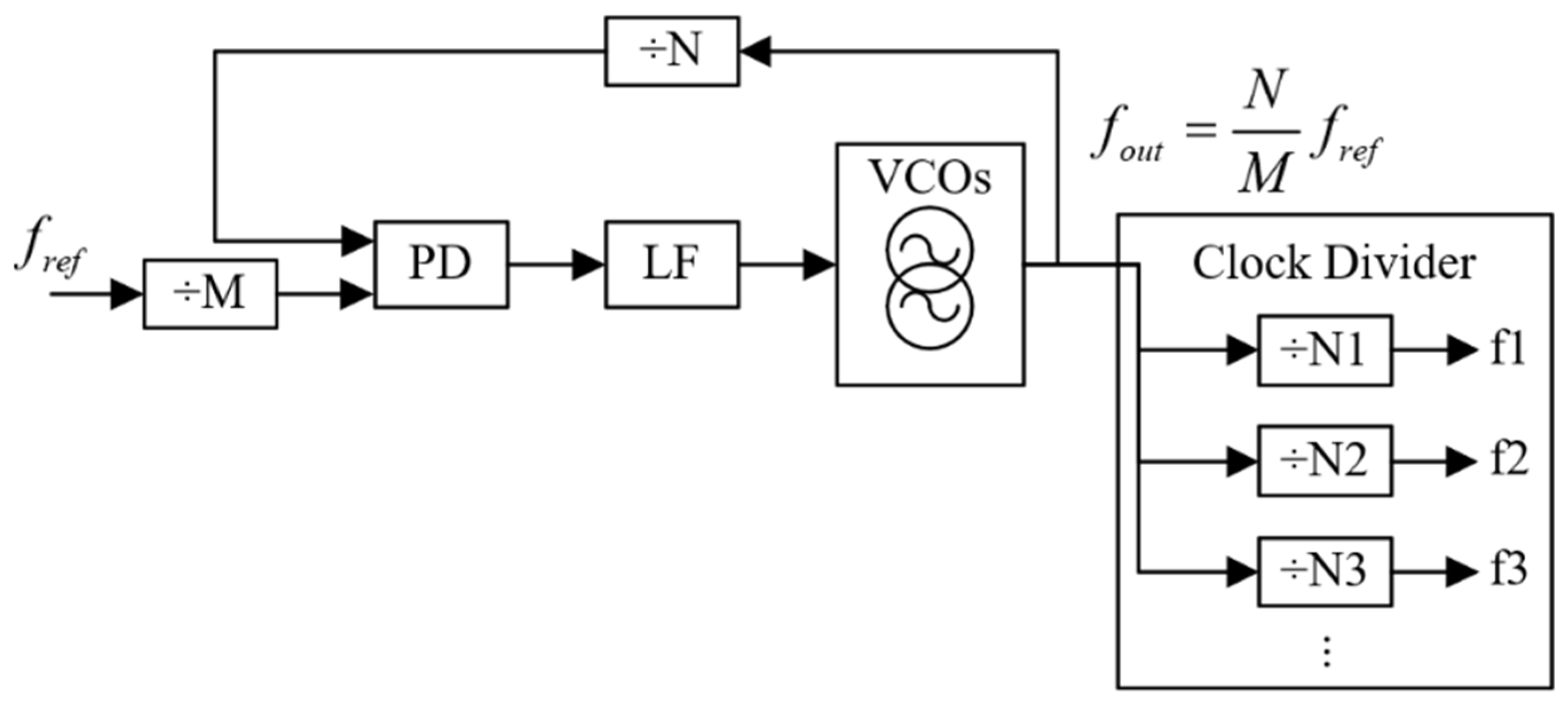
2.2. Clock Signal Generation Principle
As shown in
Figure 4, after the reference signal is input to the chip’s PLL module via the OSCin pin, a PD first compares the reference signal with the feedback signal and generates an error voltage corresponding to the phase difference. This voltage is then filtered by an LF to remove high-frequency noise and used to drive a VCO to adjust the output frequency, thereby achieving phase lock and frequency synthesis through a closed-loop feedback system. Benefiting from the chip’s built-in dual-PLL architecture, the module supports various reference frequency inputs (10 MHz–200 MHz), and by configuring different multiplication factors (integer or fractional mode), the VCO can generate stable GHz-range high-frequency clock signals in the 2370–2630 MHz and 2920–3080 MHz bands.
On the signal output side, the chip integrates 14 independent clock output channels, each equipped with a high-precision digital frequency divider. Each output channel supports the independent configuration of division ratios and drive levels. The division parameters can be flexibly set via the SPI interface to generate pilot tones and ultra-stable system clocks at various frequencies according to experimental requirements.
5. Summary and Outlook
This paper proposes the design and implementation of an STJNSS, developed to meet the demanding requirements of current space-based gravitational wave detection missions. Specifically, the system allows flexible parameter adjustment of high-frequency signals for inter-satellite clock noise transfer, system clock signals for phasemeters, and pilot tones used to suppress ADC sampling timing jitter. The STJNSS is built upon the TI LMK04828 clock chip, which can flexibly generate GHz-level clock signals within two frequency bands: 2370–2630 MHz and 2920–3080 MHz. By configuring the chip’s internal programmable dividers (supporting division ratios from 1 to 32), it can provide various output frequencies, including pilot tones (e.g., 75 MHz) and ultra-stable system clocks (e.g., 80 MHz). In addition, the integrated SYSREF divider supports division ratios ranging from 8 to 8191, enabling an output of pilot tone signals as low as 3 kHz, fully covering the frequency range required by the phasemeter. The output amplitude of the system can also be flexibly configured using external RF amplifiers (such as ZX60-33LNR-S+), with actual output amplitudes ranging from 1 V to 5 V, thereby satisfying the phasemeter’s interface drive requirements.
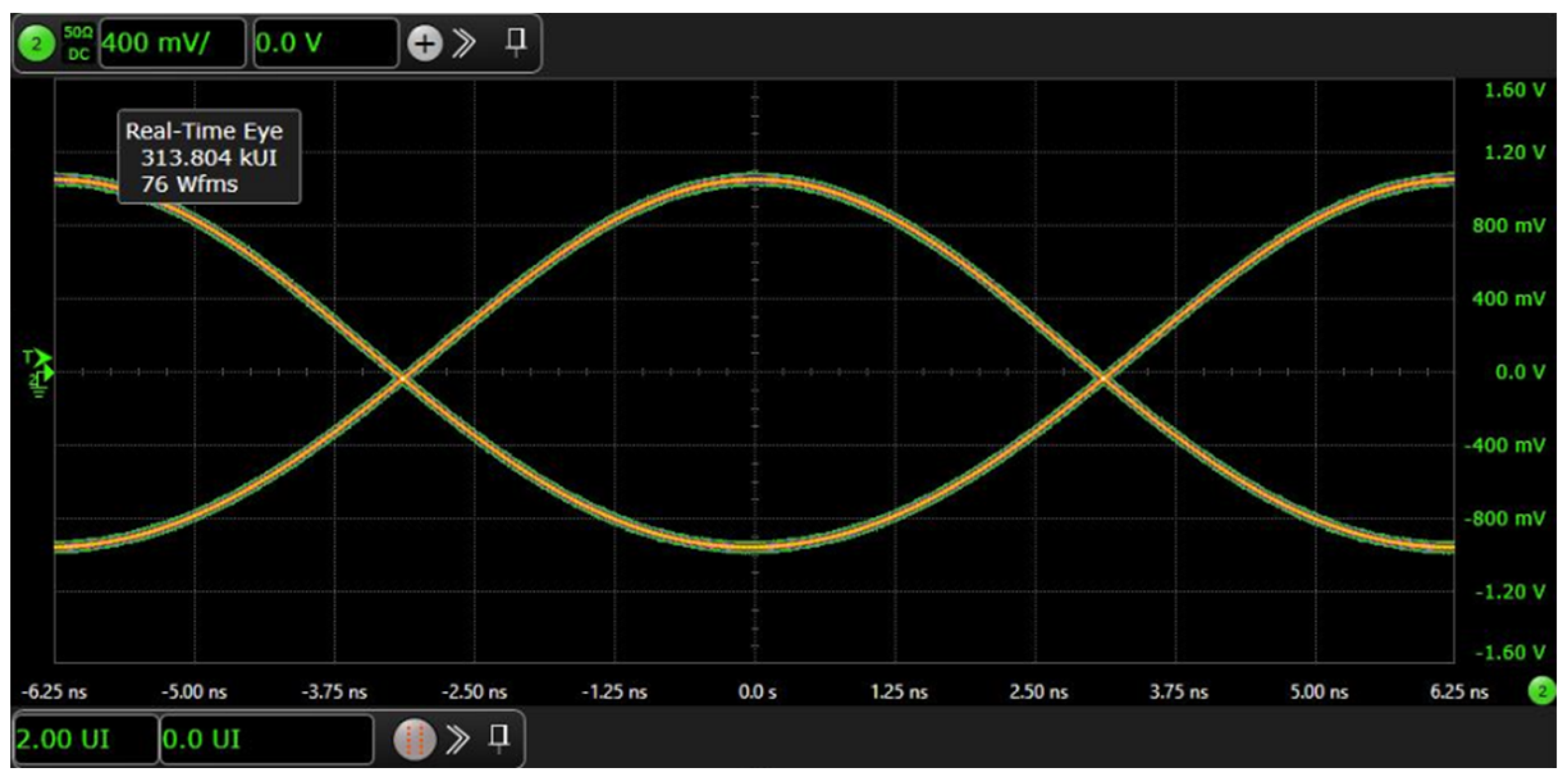
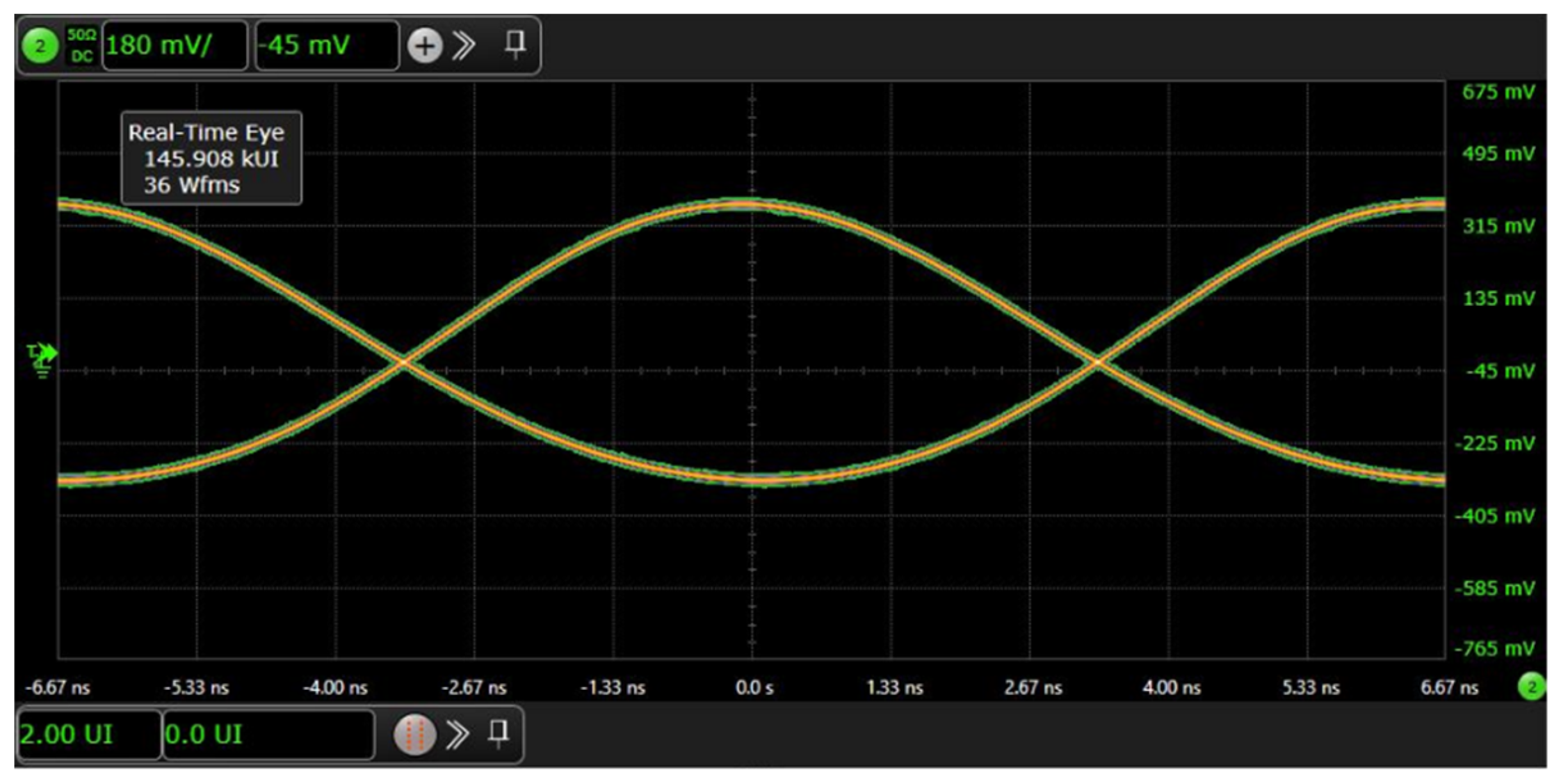
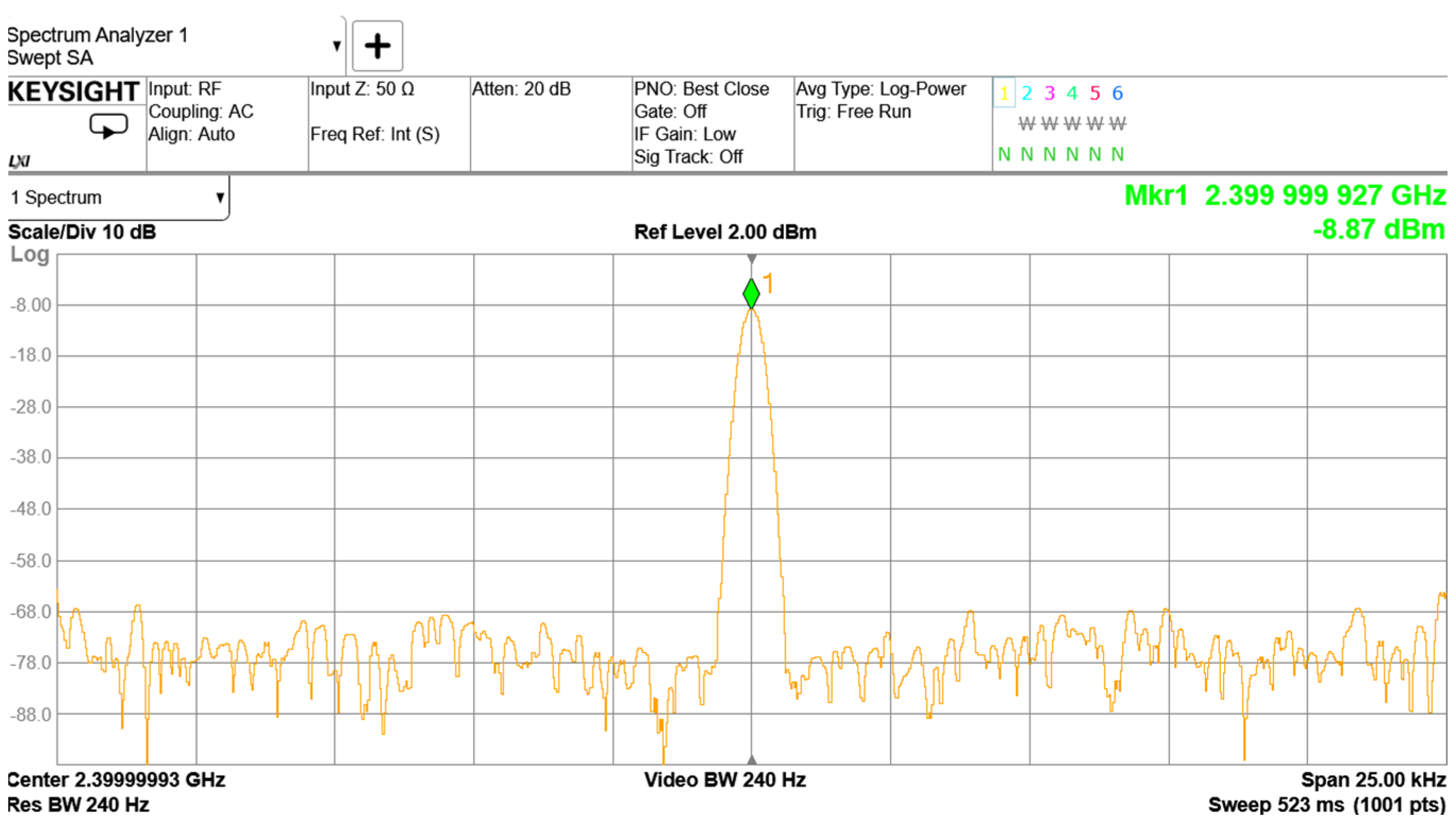
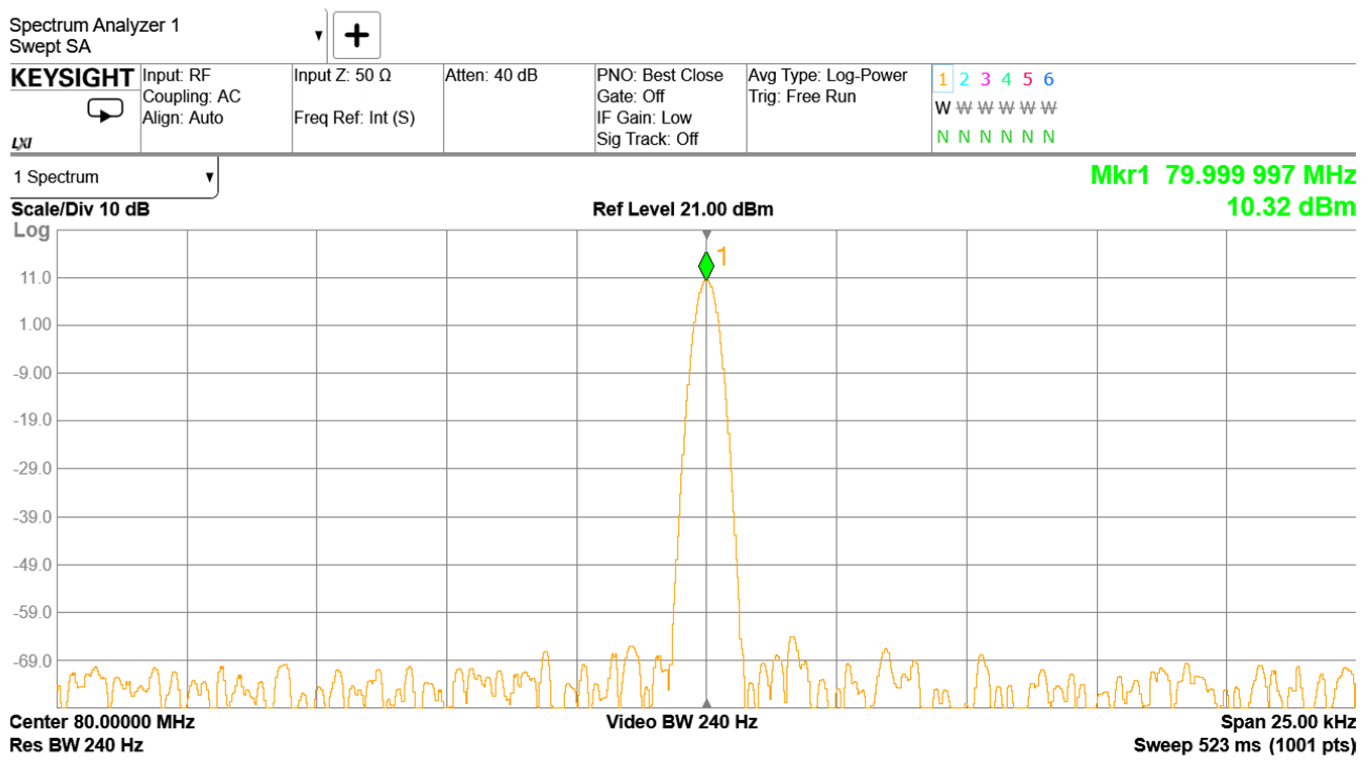
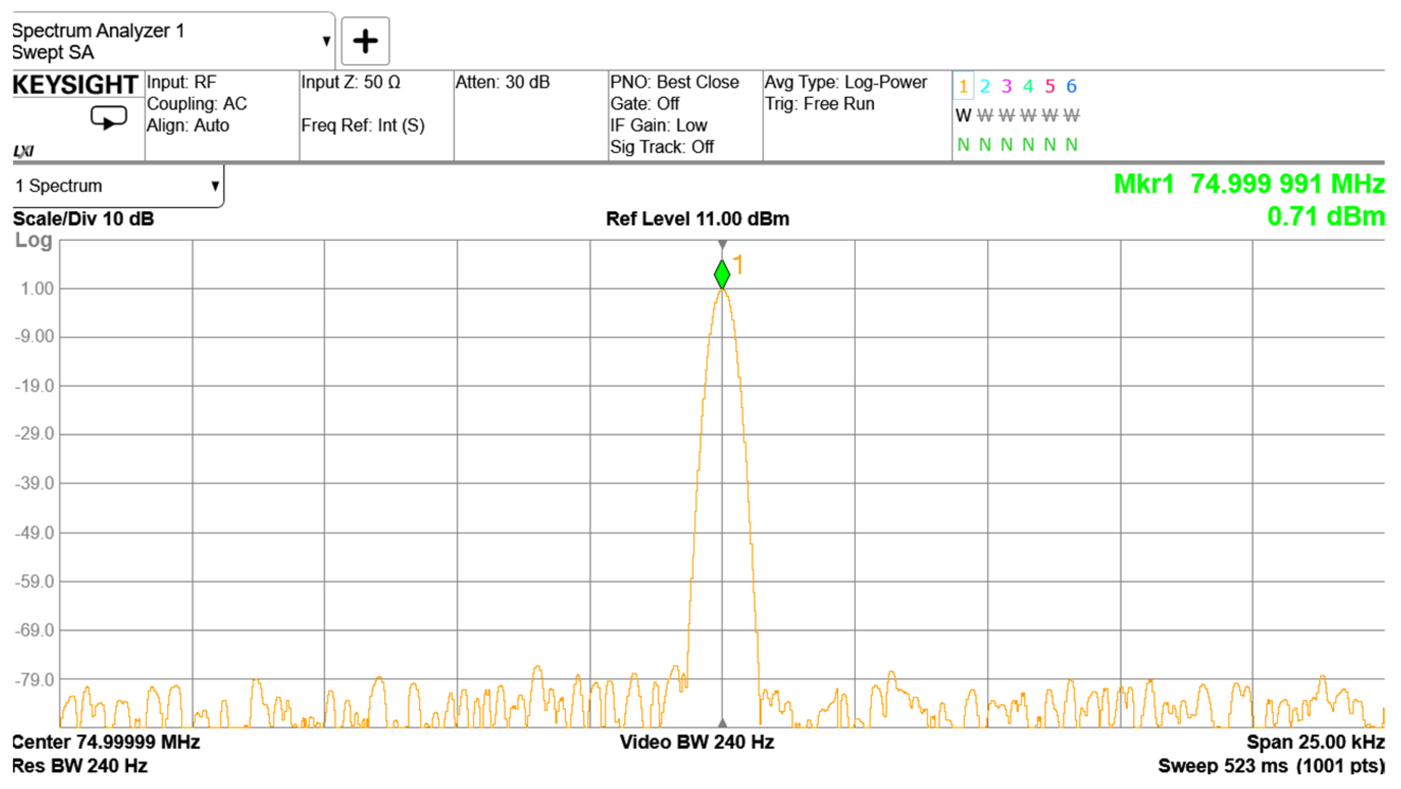
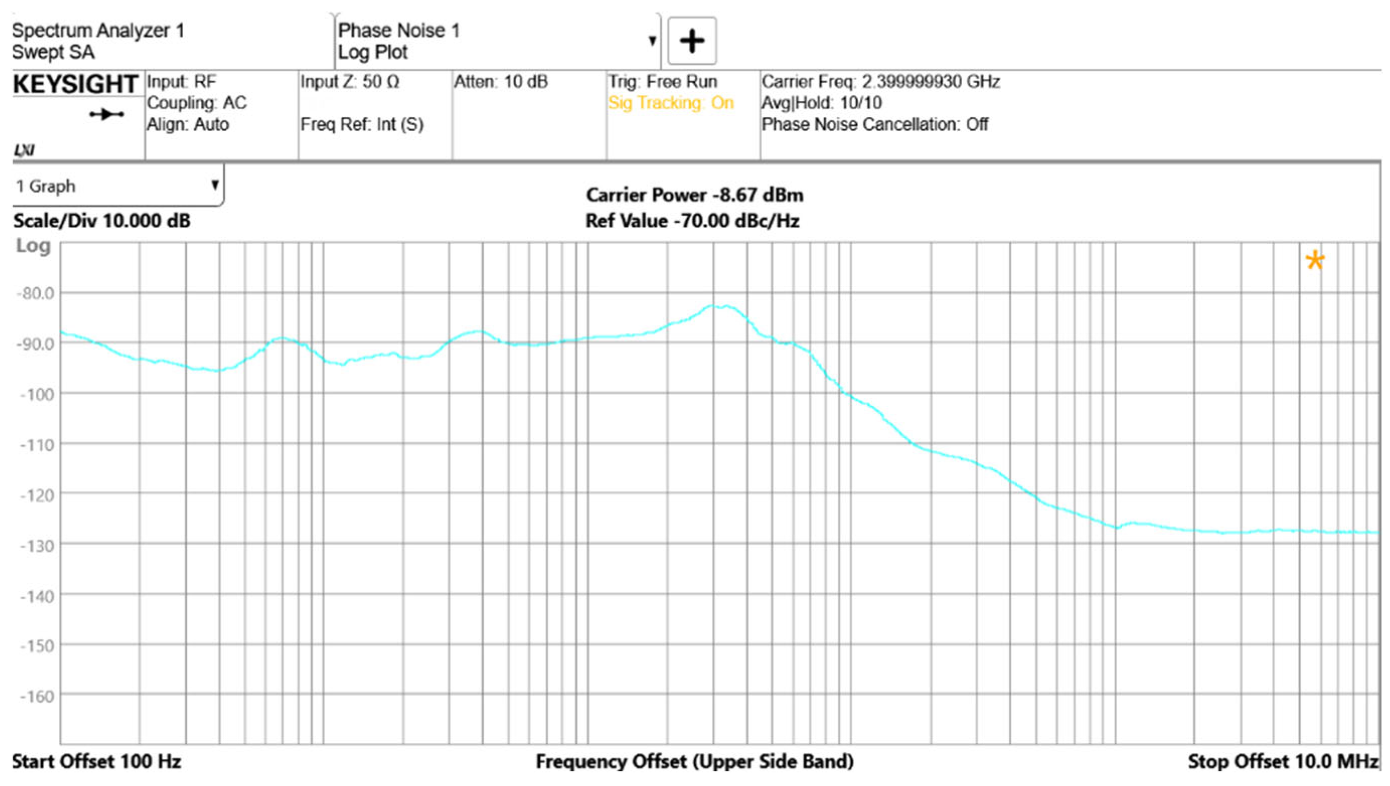
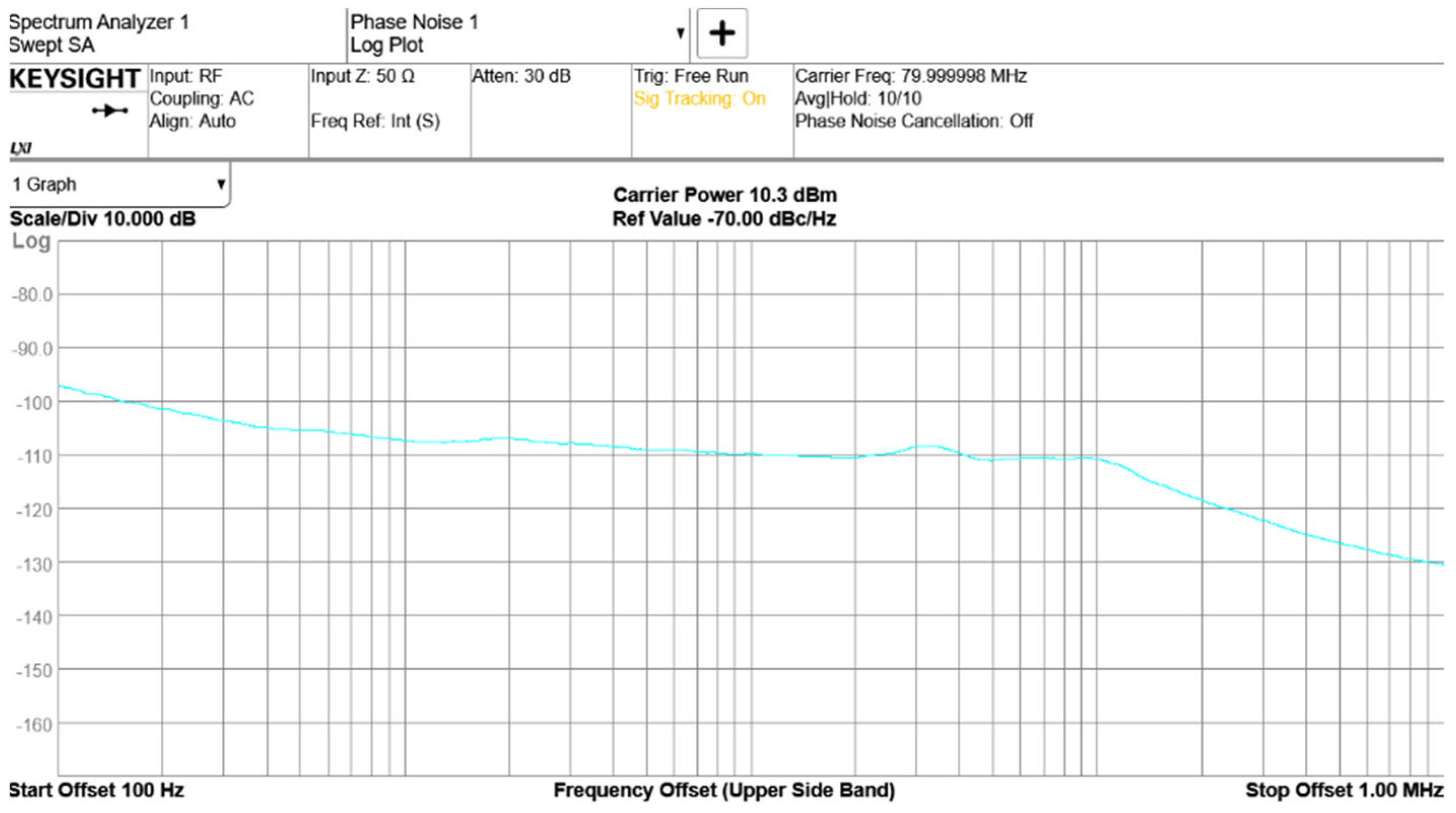
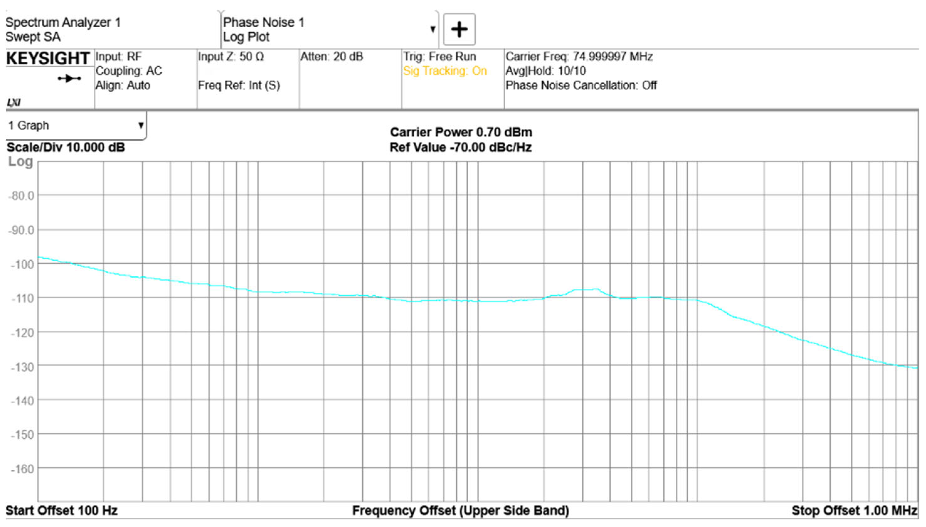
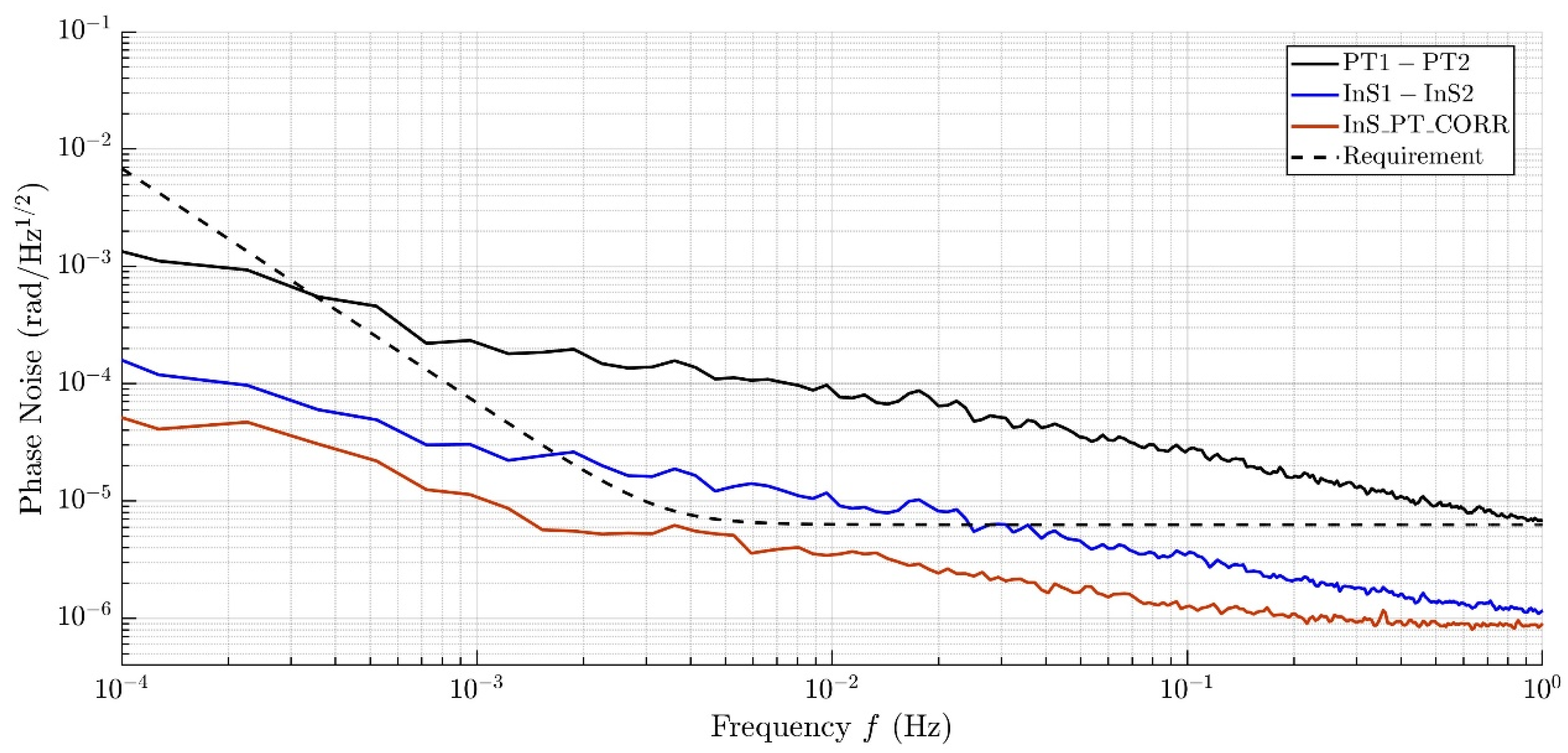
To validate the practical performance of the STJNSS, it was integrated with a phasemeter, and phase noise evaluation experiments were conducted. In the experiment, the pilot tone frequency was set to 75 MHz, the system clock to 80 MHz, and the heterodyne signal to 10 MHz. The results show that the phase meter achieves phase noise better than 2π μrad/Hz¹ᐟ² in the 0.1 mHz–1 Hz frequency range, meeting and even exceeding the performance requirements of space-based gravitational wave detection missions in the low-frequency regime. This confirms that the STJNSS can effectively suppress sampling timing jitter noise and demonstrates the feasibility of its engineering implementation.
Given that inter-satellite scientific interferometers must simultaneously support functions such as coupled relative ranging, absolute ranging, laser communication, and clock noise transfer, the phasemeter is required to simultaneously measure the phases of the main beat note and two sidebands, while also demodulating the laser communication signal. The STJNSS developed in this work significantly enhances the timing performance of the phasemeter system, laying a solid technical foundation and providing a reliable development and validation platform for future functional extensions. This demonstrates the system’s strong potential for engineering application in space missions.
6. Discussion
The space-based gravitational wave detection mission employs a three-satellite formation, with inter-satellite distances reaching hundreds of thousands to millions of kilometers. According to the principle of laser heterodyne interferometry, minute changes in the distances between inertial reference points of the satellites induced by gravitational wave events are converted into phase changes in the heterodyne interference signals, which are measured by the phasemeter. The mission requires a ranging accuracy of 1 picometer and a corresponding phase noise performance of 2π μrad/√Hz within the frequency range of 0.1 mHz to 1 Hz. Due to the inter-satellite Doppler effect, the dynamic frequency range of the heterodyne signals spans from 5 MHz to 25 MHz. To suppress sampling clock jitter noise introduced during digitization, our previous work proposed and verified a single pilot tone-based jitter noise suppression architecture, which demonstrated effective phase noise performance meeting the mission requirements within this dynamic frequency range.
Building on this foundation, this paper further develops and integrates the STJNSS as a key submodule within the phasemeter system. The STJNSS not only achieves the effective suppression of sampling timing jitter across a wide frequency dynamic range but also provides high-precision, configurable system clock and pilot tone outputs, thereby ensuring long-term timing and frequency stability of the system. The experimental results show stable phase noise performance at 10 MHz, further validating the feasibility and robustness of the single pilot tone jitter suppression architecture. This achievement significantly enhances the phasemeter system’s integration capability and engineering adaptability, laying a solid technical foundation for its application in future space-based gravitational wave detection missions.


