Abstract
In this paper, we propose and demonstrate a liquid crystal on silicon (LCoS) device that achieves high-efficiency, broadband, polarization-independent phase modulation by integrating a metasurface between the liquid crystal layer and the backplane of a commercial LCoS device. The metasurface is composed of rectangular silicon pillars encapsulated in silicon dioxide. By precisely adjusting the orientation and dimensions of these silicon pillars, the metasurface effectively controls the polarization state of the incident light, enabling polarization-independent phase modulation across the C+L band. Experimental results show that the polarization conversion ratio remains approximately 95% throughout the entire C+L band under varying driving voltages. Due to the low absorption characteristics of silicon and silicon dioxide, the metasurface integration introduces minimal loss. Additionally, the experimental results indicate that the reflectance of the metasurface-integrated LCoS exceeds 96% of the original LCoS reflectance. Notably, the metasurface does not affect the phase modulation characteristics of the device or exacerbate the fringing field effect, which could otherwise degrade modulation efficiency. The fabrication process for incorporating the silicon metasurface into the LCoS is fully compatible with standard semiconductor manufacturing techniques, thus facilitating the potential for large-scale production. Theoretical analysis further confirms that the design is tolerant to fabrication errors.
1. Introduction
The liquid crystal on silicon (LCoS) is based on liquid crystal (LC) display technology and silicon-based integrated circuits. It operates by combining the LC layer and the silicon-based backplane, integrating the pixelated metal mirror array and the drive circuit. By varying the applied external electric field, the alignment of LC molecules is controlled, and the amplitude, phase, and polarization states of the incident light are manipulated [1]. Compared to amplitude-modulating LCoS devices (mainly for video and image projections), phase-only modulating LCoS devices [2,3] have a wider range of applications, including correction of chromatic aberration in imaging systems [4], phase control in biological optical microscopy [5], wavefront correction in adaptive optics systems [6,7], and spectral shaping [8]. Additionally, phase-only modulating LCoS devices also find significant applications in fields such as laser processing [9] and holography [10].
LCoS devices offer high-resolution and broad-band continuous phase modulation owing to the pixel addressing capability and the efficient control of LC molecules. However, there are some issues to be addressed, such as the adverse impacts of zero-order light due to the gaps between the neighboring pixels and the polarization dependence of incident light. Recently, pixelated metasurfaces have emerged as a focal point of significant research and application interest [11,12]. The integration of metasurfaces with LCoS devices not only enables precise light manipulation at subwavelength scales but also augments the degrees of freedom available, thereby improving the overall performance of LCoS systems. For example, to eliminate zeroth-order light, a metasurface with an absorber function, specifically a metal–insulator–metal structure, has been integrated between the pixel array of the LCoS device and the CMOS driving circuitry. This integration effectively mitigates zeroth-order light interference between pixel gaps, significantly improving the modulation efficiency of the device [13].
To eliminate the polarization dependence of incident light, two primary improvement strategies have been proposed. The first employs a dual-layer liquid crystal structure with orthogonal orientations to independently modulate two orthogonal polarization states, thereby achieving polarization independence [14]. However, this approach requires precise control over thickness uniformity and alignment accuracy between the two liquid crystal layers, and the dual-layer encapsulation process significantly increases the complexity of the driving circuitry. The second strategy integrates a thin-film quarter-wave plate (QWP) between the single liquid crystal layer and the CMOS backplane [15]. Nevertheless, the conventional QWP are constrained by material birefringence dispersion, resulting in a practical operational bandwidth typically limited to less than 50 nm, while their thickness exacerbates the fringing field effect. Aiming at the limitations of the conventional QWP, the method of replacing the QWP with a plasma metasurface has also been proposed [16], but it remains questionable whether it will exacerbate the fringing field effect. In addition, the method of regulating the reflection of two incident lights with mutually perpendicular polarization directions at different positions through reflective metal gratings has also been proposed [17]. However, its structural parameters need to be strictly calculated, and there is almost no tolerance.
In this paper, a high-efficiency and broadband polarization-independent LCoS (PI-LCoS) is designed by embedding a well-designed metasurface layer between the liquid crystal layer and the backplane of a commercial phase LCoS device. The metasurface consists of rectangular high-refractive-index silicon pillars and silica as the cladding. With the excitation of incident light, the electric dipole response is generated along the long edge of the silicon pillars [18], resulting in polarization conversion when superimposed with the incident electric field. Due to the negligible absorption of silicon in the optical communication band, the optical loss introduced by the metasurface layer is almost zero. The polarization conversion ratio (PCR) was measured, yielding a value of approximately 95% across the entire C+L band and at various driving voltages, which is consistent with the simulation results. Due to the high polarization conversion efficiency of the metasurface, the LCoS can achieve polarization-independent reflection over the whole C+L telecommunication band. Furthermore, the metasurface does not interfere with the device’s inherent phase modulation properties, nor does it exacerbate the fringing field effect. Additionally, since the meta-atoms of the metasurface are made of silicon, the fabrication process is highly compatible with CMOS technology. Furthermore, additional simulation results indicate that variations of ±20 nm in the length and ±10 nm in the width of the silicon pillars around design values have a minimal impact on the polarization conversion ratio. This feature offers significant process flexibility, which is advantageous for mass production.
2. Design Principle
The overall configuration of the PI-LCoS device is depicted in Figure 1a. The metasurface layer is located between the LC layer and the backplane. When light is incident on the LCoS device, it is phase-modulated by the LC layer, which introduces a phase difference between the two orthogonal linear polarizations of the incident light due to the electrically controlled birefringence effect. The metasurface layer, in conjunction with the backplane, rotates the two orthogonal linear-polarized states of the incident light by 90 degrees after reflected, ensuring that both orthogonal linear polarizations are equally phase-modulated during the double-pass of the LC layer, and thus achieving polarization-independent phase modulation. The metasurface is configured as a periodic array of square cells, with each unit cell constituted by rectangular silicon pillars covered by SiO2 cladding, as depicted in Figure 1b. The direction of the silicon pillars forms an angle of with the x-axis.
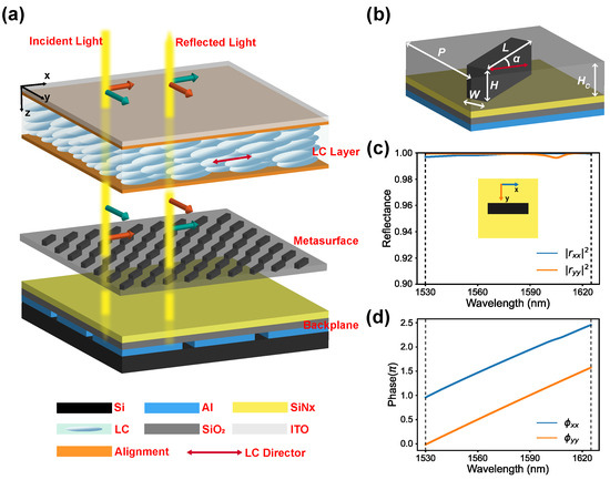
Figure 1.
(a) Structural diagram of the polarization-independent LCoS device. (b) Structure diagram of the metasurface unit, composed of rectangular silicon pillars and a SiO2 cladding, with a structural period nm, pillar length nm, width nm, height nm, and SiO2 cladding height nm. The angle between the silicon rectangular pillars and the LC alignment direction is denoted as . (c,d) The reflectivity and phase of the incident x-polarized and y-polarized light after reflection by the backplane integrating the metasurface in the case of .
The incorporation of silicon pillars leads to differing effective refractive indices in the length L and width W directions. As a result, the incident lights in these two polarization directions undergo varying phase delays, altering the polarization state. Incorporating the reflection from the LCoS backplane, the cell unit serves as a reflective wave plate. To clarify the wave plate mechanism, considering the scenario of . The top view of the unit is shown as the inset of Figure 1c, with the size of the silicon pillar of nm, nm, and nm, where L is aligned along the x-axis. The simulation results with the finite element method show that the reflectivities and are nearly 100%, as shown in Figure 1c. Moreover, the phase difference between the two orthogonal polarizations is consistently , which is wavelength-independent, as indicated in Figure 1d. The backplane integrating the metasurface acts as a reflective half-wave plate with its fast axis oriented along the y-axis, which can be represented by the Jones matrix as . Consider the case where L forms an angle of with the x-axis, implying that the silicon pillar is rotated around the z-axis by , which corresponds to a rotation of the fast axis of the reflective half-wave plate by degrees. The corresponding transmission matrix is given by
Setting , it becomes clear that , indicating that the incident light is transformed into an orthogonal polarization state upon reflection by the backplane integrating metasurface.
In the PI-LCoS device, the LC layer is composed of nematic liquid crystal with positive uniaxiality [19]. With the alignment layer, the LC director is oriented along the x-axis when no voltage is applied between the ITO layer and the backplane, while the LC director aligns along the x-axis. When a voltage is applied, the LC director rotates around the y-axis, with the rotation angle being voltage-dependent, as shown in Figure 2a. Due to the rotation of the LC director, the LC layer exhibits anisotropy, resulting in varying refractive indices along the three orthogonal axes. The relationship of these refractive indices with the rotation angle is described by , , and [20], where is the refractive index in the LC direction, and is the refractive index perpendicular to the LC direction. When light is incident in the LCoS device along the z-axis, the and polarization components exhibit a phase difference of , where d is the thickness of the LC layer, and is the incident wavelength. The reflection of light throughout the entire LCoS device can be characterized using the transfer matrix as
which implies that the polarization-independent phase modulation is achieved by the LCoS device. The phase modulation is achieved within each pixel of the LCoS device, with the modulation depth being determined by the voltage across the pixel’s electrodes, allowing for the pixel-level phase modulation. Each actually corresponds to a unique at that voltage.
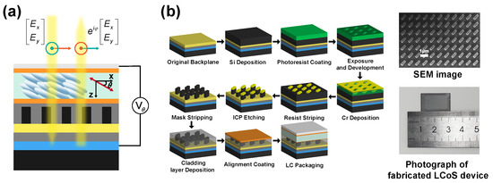
Figure 2.
(a) Schematic diagram of the device structure and optical path within a single pixel. (b) The fabrication process of metasurfaces. The insets are the SEM image of the metasurface and an LCoS sample.
3. Experimental Results and Discussion
3.1. Fabrication and Optical Property Measurement
To verify the design, we fabricated a PI-LCoS phase-modulating device based on a commercial liquid crystal spatial light modulator with an operating wavelength of 1400–1700 nm (Model: PLUTO-2-TELCO-013, by HOLOEYE Photonics AG.) with semiconductor manufacturing processes. The fabrication process is depicted in Figure 2b. First, a silicon layer with a thickness of 460 nm was deposited on the backplane of a commercial LCoS device using an Oxford Plasma100 Pro (Oxford Instruments, Oxford, UK) plasma-enhanced chemical vapor deposition (PECVD) system, with silane (5% SiH4/Ar mixed gas) as the source gas. The substrate temperature was maintained at 300 °C, and the chamber pressure was controlled between 100–200 mTorr. Subsequently, a photoresist film with a thickness of 250 nm was formed by spin-coating positive photoresist (AR-P 6200.09, Allresist GmbH, Berlin, Germany) onto the silicon layer using a Suss automatic spin coater at 5000 rpm for 60 s. The coated substrate was then baked at 150 °C for 1 min to cure the photoresist. Next, lithography exposure was performed using an ELIONIX-FS 125G8 (ELionix, Tokyo, Japan) electron beam lithography system with an acceleration voltage of 125 kV and an exposure dose of 100–200 . After exposure, the sample was developed by immersion in an AR 600-546 developer for 63 s, followed by rinsing with deionized water for 30 s. Thereafter, a chromium (Cr) layer with a thickness of 30 nm was deposited on the developed photoresist using a ULVAC ei-5z-1 (ULVAC, Maosaki, Japan) electron beam evaporation system under a vacuum below Torr and an evaporation rate of 1 Å/s. The sample underwent ultrasonic-assisted liftoff in an N-methyl-2-pyrrolidone (NMP) solution at dual frequencies of 40 and 50 kHz for 60 min to remove excess photoresist and Cr, resulting in a Cr-mask. Inductively coupled plasma (ICP) etching was performed using a Leuven ICP etch system with SF6, CHF3, and Ar gases (flow ratio 4:5:2 sccm) at 100 W RF of power, 10 mTorr of pressure, and an etching time of 85 s (etching rate = 5 nm/s), resulting in silicon pillars with heights of 460 nm. The Cr mask was removed by immersion in a chromium etchant for 1 min. A SiO2 cladding layer with a thickness of 500 nm was deposited using the PECVD system at 300–400 °C and 150–250 mTorr with SiH4 and N2O as source gases. Surface planarization was achieved via a Logitech Limited chemical mechanical polishing (CMP) system using Al2O3 slurry (50 nm particle size, pH = 10) under 1 psi of pressure, a 100 rpm rotation speed, and 5 min of polishing time, completing the metasurface layer fabrication on the LCoS backplane, with the SEM image shown in the inset of Figure 2b. Finally, a PI-LCoS device is prepared by encapsulating the metasurface layer with liquid crystals, with the sample shown in the inset of Figure 2b.
The polarization conversion ratio (PCR) is a crucial parameter for the PI-LCoS phase modulator, defined as [21], where and are the power of converted and non-converted polarization light, respectively. The schematic of the setup for the PCR measurement is shown in Figure 3a. Light emitted from the laser (Model: TLX5, Thorlabs, Newton, NJ, USA), is collimated and passes through a polarizer (P1), then through the beam splitter (BS), where it is divided into two paths. One beam is incident on the LCoS and reflected, then again reflected by the BS, passing through a polarizer (P2) and a focusing lens before reaching the detector. A second beam serves as the reference. The polarization of the incident and outgoing light can be selectively controlled by rotating P1 and P2, respectively. Figure 3b presents the simulated PCR results over the entire C+L band at the whole LC refractive index modulation range (as described in [22], corresponding to the various driving voltages). It can be seen that, in the majority of the regions, PCR exceeds 96%. The experimentally obtained PCR values are somewhat lower than the simulated values, primarily because of the omission of process-related factors that affect the PCR in the simulation. The PCR measurements were conducted for wavelengths ranging from 1520 to 1630 nm at various LCoS driving voltages, as shown in Figure 3c. The results clearly demonstrate that PCR is approximately 95% across the entire range of LCoS drive voltages for all wavelengths. Figure 3d illustrates the simulated absorption curve of light after reflection by the backplane integrating metasurface, indicating that the metasurface exhibits negligible light absorption. Reflectivity measurements were conducted for the PI-LCoS and the original commercial LCoS device, denoted as and , respectively. The ratios of the two reflectivities at various driving voltages are shown in Figure 3e. The ratios, at five different wavelengths covering the entire C+L band, remain above 96% throughout the LC driving voltage range, indicating a slight reduction in reflectivity due to the incorporation of the metasurface layer. This is attributed to the low absorption of silicon in the near-infrared spectra, which gives the metasurface the advantage of low loss. All of these simulation results were obtained by using the frequency-domain solver in the finite element simulation software CST 2023. The reflectance of co-polarized and cross-polarized light can be calculated based on the obtained S parameters.
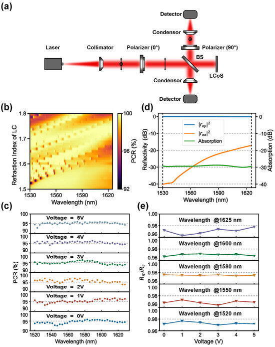
Figure 3.
(a) Schematic diagram of the PCR measurement setup. (b) Simulated PCR over the entire C+L band and across the whole LC refractive index modulation range. (c) Experimental PCR values at wavelengths ranging from 1520 to 1630 nm. (d) The simulated reflectivity curves for co−polarized and cross−polarized light, as well as the absorption rate, of incident light polarized along the x−direction after reflection. (e) The experimentally measured reflectivity ratios of the LCoS integrated with the metasurface () and the original LCoS ().
3.2. Phase Response Measurement
The phase responses of both the original LCoS device and the PI-LCoS device integrated with the metasurface were measured. The experimental setup is shown in Figure 4a. The incident light, with a wavelength of 1550 nm, was irradiated onto the entire LCoS panel following beam expansion. A polarizer was employed to ensure that the polarization direction of the incident light remained consistent across both experiments. The LCoS panel was divided into two regions: the upper region was applied with a single phase, while the lower region was subjected to a periodic phase modulation with a period of 4 pixels and a phase difference of between adjacent pixels. The lower region of the LCoS effectively acted as a phase grating, with its order diffracted light overlapping with the light reflected by the upper region. The diffraction angle was calculated based on the grating equation. The interference fringes generated by the overlap of the two beams were recorded at a distance cm, as determined by the equation , where W is the width of the LCoS panel, and is the first-order diffraction angle. As the gray level of the single phase region varied from 0 to 255, the interference pattern shifted accordingly. The pixels covered by the yellow line on the fringes were selected, and their intensities were recorded to obtain the fitted curves. Subsequently, the relationship between gray levels and phase response, shown in Figure 4b, was derived. The phase response of the original LCoS was halved. Specifically, the phase response of the incident light with the same polarization after passing PI-LCoS was half of the phase response of the original LCoS. Additionally, the phase responses of the PI-LCoS for the two cross-polarized incident light beams were nearly identical, confirming that the metasurface possesses a polarization conversion function and does not affect the original phase modulation characteristics.
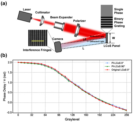
Figure 4.
(a) Schematic diagram of the phase response measurement setup. (b) The relationship between gray levels and phase response of PI−LCoS and original LCoS.
3.3. Fringing Field Effect Analysis and Beam Steering
However, it is not sufficiently rigorous to conclude that the addition of the metasurface will not exacerbate the fringing field effect based on the consistent phase response. This is because the fringing field effect typically arises when there is a significant voltage difference between adjacent pixels. In contrast, the phase response measurement reflects the overall modulation effect and does not provide insight into the pixel-level phase modulation. The phase modulation of LCoS is primarily dependent on the rotation angle of the LC director, which is determined by the electric potential distribution. To investigate whether metasurface exacerbate the fringing field effect and consequently alter the electric potential distribution, we simulated the potential distribution in three adjacent pixel units, each with a pixel pitch of 1 µm and an LC thickness of 8 m, while keeping other structural parameters consistent with previous descriptions. When a 5 V voltage was applied to the middle pixel, and no voltage was applied to the two adjacent pixels, the finite element software COMSOL 6.0 was used to simulate the potential distribution based on the electrostatic field theory. In the simulation software, the static dielectric constants of each material silicon were selected. The static dielectric constants of silicon and silicon dioxide were 11.7 and 3.9, respectively. The static dielectric constants of liquid crystal at a 5 V voltage and without voltage were set to 2.25 and 3.24, respectively. The results are shown in Figure 5a. The top image in Figure 5a depicts the potential distribution of the original LCoS. For comparison, the bottom image shows the potential distribution for the LCoS with metasurface. These two distributions are nearly identical, suggesting that the integrated metasurface has a negligible effect on the potential distribution within the device.
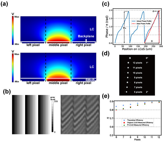
Figure 5.
(a) The simulated electric potential distributions of the original LCoS, and the LCoS with metasurface. (b) Gray level of blazed grating imposed on the LCoS (left) and a single white light interference pattern captured by the interferometer when the corresponding gray level was applied (right). (c) The phase profile within a single period when the grating period is 12 pixels. (d) The measured light intensity distributions after the beam steering. (e) The theoretical and experimentally measured diffraction efficiencies of the original LCoS and the PI-LCoS.
To verify this, we imposed a blazed grating onto the LCoS and conducted beam steering experiments at a wavelength of 1550 nm. Pixel-level phase observations were successfully achieved using white light interference. Since white light interference requires ensuring that the polarization directions of the reference light and the reflected light passing through the LCoS are aligned, a white light interferometer with a central light source wavelength of nm was selected. This wavelength is far outside the C+L band, which possesses the polarization conversion function. According to the principle of Michelson interference, after the incident light passes through the LCoS, an additional optical path difference will be generated, causing a shift in the zero optical path difference position and generating an additional height . The relationship between these two parameter is given by . White light interference images were captured at various distances as the LCoS was moved along the optical axis direction under the control of a piezoelectric transducer, with a step size of . By analyzing multiple white light interference images of a single pixel, the white light interference signal for that single pixel was obtained. The position corresponding to the maximum signal intensity represents the zero optical path difference value. For this, the actual phase modulation amount, , at the wavelength of nm can be calculated. The phase modulation at a wavelength of 1550 nm could be obtained by , where and are the birefringence values of the LC at the two wavelengths respectively [22]. The left image in Figure 5b shows the gray level imposed on the LCoS, while the right image displays a single white light interference pattern captured by the interferometer when the corresponding gray level was applied. In white light interferometry, the intensity of the same pixel varies across different interference images. Therefore, it is necessary to control the piezoelectric transducer to take multiple images to ensure that all pixels within a single period of the blazed grating reach the maximum brightness. By recording the corresponding displacements of the piezoelectric transducer when each pixel achieves maximum intensity, the phase differences between pixels can be derived from these displacement values. Measurements were carried out for blazed gratings with periods ranging from 6 to 12 pixels. Figure 5c presents the phase profile within a single period when the grating period is 12 pixels. It can be observed that the maximum value of the actual phase profile is less than 2, and a flyback region is presented. The diffraction efficiency of the imposed blazed grating is given by [23]
where m is the diffraction order, D is the grating period, d is the length of the flyback region, and is the maximum phase modulation amount. The measured light intensity distributions after the beam steering are shown in Figure 5d. Subsequently, when the diffraction order , the theoretical values of the diffraction efficiency under different grating periods and the diffraction efficiency values measured for the original LCoS and the PI-LCoS are obtained, as shown in Figure 5e. It can be seen that the diffraction efficiency of the PI-LCoS integrated with the metasurface is almost the same as that of the original LCoS, and it does not exacerbate the fringing field effect.
3.4. Processing Tolerence
In the actual fabrication process, discrepancies between the actual and the design values may occur due to process errors [24]. Achieving a high tolerance for these process errors is a key objective in device design. In the proposed PI-LCoS, the width and length of the silicon pillars of the metasurface are two parameters that are particularly susceptible to variations. When the width W of the silicon pillars varies within nm and the length L varies within nm, the PCR performance of the LCoS was simulated, as shown in Figure 6. It can be seen that the PCR is greater than 97.5% throughout the C + L band, indicating that there is a process tolerance of nm for the width and nm for the length of the silicon pillars. Meanwhile, it can be seen that the resonance peaks in Figure 6 originate from the guided mode resonances of the silicon pillars, which are determined by the matching relationship between the width of the silicon pillars and the wavelength of the incident light. The silicon pillars and silica cladding form a high-low refractive index waveguide structure. When the incident light wavelength matches the width and period of the silicon pillars, guided modes within the pillars are excited (such as transverse modes corresponding to TE or TM polarization), leading to strong resonant responses at specific wavelengths. These resonance peaks enhance the polarization conversion efficiency at target wavelengths. The presence of the resonance peaks not only does not significantly degrade the device performance, but also optimizes the applicability of LCoS in optical communication and other scenarios by selectively enhancing polarization conversion in key bands. This phenomenon is consistent with the guided mode resonance theory of dielectric metasurface, and the experimental results verify the rationality of the design and process robustness.
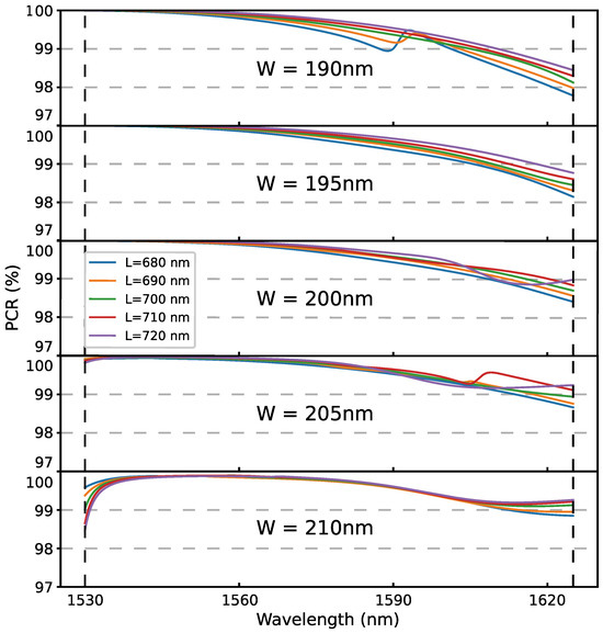
Figure 6.
The PCR varies with different silicon pillar dimensions across the entire C+L band.
4. Conclusions
We have successfully integrated silicon-based metasurfaces with commercial LCoS devices, overcoming the narrow-bandwidth limitation of QWP and achieving polarization-independent phase modulation across the C+L band. This integration eliminates the need for complex polarization optical elements, thereby simplifying the LCoS. The silicon-based metasurface introduced in this study has a relatively high polarization conversion rate, and the absorption in the communication band can be ignored. Our PCR result is 95%, which is comparable to that of the reference [16], but the reflectance is higher than 96%, which is superior to their work. Meanwhile, we observed pixel-level phase modulation through white light interference, which more rigorously proves that the silicon-based metasurface does not exacerbate the fringing field effect and thus preserves the internal potential distribution of the LCoS device. As a result, the original driving voltage requirements and optical performance of the device are maintained. Furthermore, the silicon is highly compatible with standard semiconductor fabrication processes, and the design demonstrates substantial tolerance to variations in the size of the metasurface elements. These attributes underscore the significant potential for large-scale production and commercialization of PI-LCoS devices. By simplifying the overall optical system, this work opens new avenues for a variety of practical applications.
Author Contributions
Conceptualization, Y.D.; Methodology, Y.D.; Formal analysis, B.L.; Investigation, B.L.; Data curation, B.L.; Writing-original draft, Y.D.; Writing-review, J.Y.; Visualization, Y.D. and J.Y.; Supervision, J.Y. All authors have read and agreed to the published version of the manuscript.
Funding
This work was supported by the Research Project at Zhejiang University of Technology (KYY-HX-20230664 and KYY-HX-20230664-1).
Institutional Review Board Statement
Not applicable.
Informed Consent Statement
Not applicable.
Data Availability Statement
Data underlying the results presented in this paper are not publicly available at this time but can be obtained from the authors upon reasonable request.
Conflicts of Interest
The authors declare no conflicts of interest.
References
- Vettese, D. Liquid crystal on silicon. Nat. Photon 2010, 4, 752–754. [Google Scholar] [CrossRef]
- Zhang, Z.; You, Z.; Chu, D. Fundamentals of phase-only liquid crystal on silicon (LCOS) devices. Light Sci. Appl. 2014, 3, e213. [Google Scholar] [CrossRef]
- Lazarev, G.; Chen, P.J.; Strauss, J.; Fontaine, N.; Forbes, A. Beyond the display: Phase-only liquid crystal on Silicon devices and their applications in photonics [Invited]. Opt. Express 2019, 27, 16206. [Google Scholar] [CrossRef]
- Fernández, E.J.; Prieto, P.M.; Artal, P. Wave-aberration control with a liquid crystal on silicon (LCOS) spatial phase modulator. Opt. Express 2009, 17, 11013–11025. [Google Scholar] [CrossRef] [PubMed]
- Yamaguchi, K.; Otomo, K.; Kozawa, Y.; Tsutsumi, M.; Inose, T.; Hirai, K.; Sato, S.; Nemoto, T.; Uji-i, H. Adaptive Optical Two-Photon Microscopy for Surface-Profiled Living Biological Specimens. ACS Omega 2021, 6, 438–447. [Google Scholar] [CrossRef]
- Fernandez, E.J.; Suchkov, N.; Artal, P. Adaptation to the eye’s chromatic aberration measured with an adaptive optics visual simulator. Opt. Express 2020, 28, 37450–37458. [Google Scholar] [CrossRef]
- Eguchi, A.; Brewer, J.; Milster, T.D. Optimization of random phase diversity for adaptive optics using an LCoS spatial light modulator. Appl. Opt. 2019, 58, 6834–6840. [Google Scholar] [CrossRef]
- Guo, X.; Liu, Y.; Yin, T.; Morrison, B.; Pagani, M.; Daulay, O.; Bogaerts, W.; Eggleton, B.J.; Casas-Bedoya, A.; Marpaung, D. Versatile silicon microwave photonic spectral shaper. APL Photonics 2021, 6, 036106. [Google Scholar] [CrossRef]
- Hasegawa, S.; Hayasaki, Y. Femtosecond laser processing with adaptive optics based on convolutional neural network. Opt. Lasers Eng. 2021, 141, 106563. [Google Scholar] [CrossRef]
- Han, Z.; Yan, B.; Qi, Y.; Wang, Y.; Wang, Y. Color holographic display using single chip LCOS. Appl. Opt. 2019, 58, 69–75. [Google Scholar] [CrossRef] [PubMed]
- Yu, N.; Genevet, P.; Kats, M.A.; Aieta, F.; Tetienne, J.P.; Capasso, F.; Gaburro, Z. Light Propagation with Phase Discontinuities: Generalized Laws of Reflection and Refraction. Science 2011, 334, 333–337. [Google Scholar] [CrossRef] [PubMed]
- Zhang, C.; Hu, J.; Dong, Y.; Zeng, A.; Huang, H.; Wang, C. High efficiency all-dielectric pixelated metasurface for near-infrared full-Stokes polarization detection. Photon. Res. 2021, 9, 583–589. [Google Scholar] [CrossRef]
- Zhang, Y.; Wu, Z.; Xia, J.; Wu, J.; Yang, K.; Dong, C.; Tong, G.; Zhang, H.; Yang, R.; Luo, Y. Infrared metasurface absorber based on silicon-based CMOS process. Opt. Express 2022, 30, 32937–32947. [Google Scholar] [CrossRef]
- Lin, Y.H.; Ren, H.; Wu, Y.H.; Zhao, Y.; Fang, J.; Ge, Z.; Wu, S.T. Polarization-independent liquid crystal phase modulator using a thin polymer-separated double-layered structure. Opt. Express 2005, 13, 8746–8752. [Google Scholar] [CrossRef]
- Moore, J.R.; Collings, N.; Crossland, W.A.; Davey, A.B.; Evans, M.; Jeziorska, A.M.; Komarcevic, M.; Parker, R.J.; Wilkinson, T.D.; Xu, H. The Silicon Backplane Design for an LCOS Polarization-Insensitive Phase Hologram SLM. IEEE Photonics Technol. Lett. 2008, 20, 60–62. [Google Scholar] [CrossRef]
- Zhu, Z.; Wen, Y.; Li, J.; Chen, Y.; Peng, Z.; Li, J.; Zhu, L.; Wu, Y.; Zhou, L.; Liu, L.; et al. Metasurface-enabled polarization-independent LCoS spatial light modulator for 4K resolution and beyond. Light Sci. Appl. 2023, 12, 151. [Google Scholar] [CrossRef] [PubMed]
- Anderson Keith, J.M.M. Reflective LC Devices Including Thin Film Metal Grating. U.S. Patent 10,473,839 B2, 12 November 2019. [Google Scholar]
- Sakhare, P.A.; Atmakuri, M.; Dontabhaktuni, J. Tailoring the resonant modes in liquid crystal based all-dielectric metasurfaces. Sci. Rep. 2023, 13, 6780. [Google Scholar] [CrossRef]
- Gelbart, W.M. Molecular theory of nematic liquid crystals. J. Phys. Chem. 1982, 86, 4298–4307. [Google Scholar] [CrossRef]
- Ramachandran, G.N.; Ramaseshan, S. Crystal Optics; Springer: Berlin/Heidelberg, Germany, 1961. [Google Scholar]
- Liu, T.; Yang, S.; Tang, D.; Da, H.; Feng, R.; Zhu, T.; Sun, F.; Ding, W. Polarization conversion based on an all-dielectric metasurface for optical fiber applications. J. Phys. D Appl. Phys. 2017, 50, 334001. [Google Scholar] [CrossRef]
- Tkachenko, V.; Abbate, G.; Marino, A.; Vita, F.; Giocondo, M.; Mazzulla, A.; Ciuchi, F.; Stefano, L.D. Nematic Liquid Crystal Optical Dispersion in the Visible-Near Infrared Range. Mol. Cryst. Liq. Cryst. 2006, 454, 263–271. [Google Scholar] [CrossRef]
- Xu, L.; Zhang, J.; Wu, L.Y. Influence of phase delay profile on diffraction efficiency of liquid crystal optical phased array. Opt. Laser Technol. 2009, 41, 509–516. [Google Scholar] [CrossRef]
- Lee, K.B.; Cheon, S.; Kim, C.O. A Convolutional Neural Network for Fault Classification and Diagnosis in Semiconductor Manufacturing Processes. IEEE Trans. Semicond. Manuf. 2017, 30, 135–142. [Google Scholar] [CrossRef]
Disclaimer/Publisher’s Note: The statements, opinions and data contained in all publications are solely those of the individual author(s) and contributor(s) and not of MDPI and/or the editor(s). MDPI and/or the editor(s) disclaim responsibility for any injury to people or property resulting from any ideas, methods, instructions or products referred to in the content. |
© 2025 by the authors. Licensee MDPI, Basel, Switzerland. This article is an open access article distributed under the terms and conditions of the Creative Commons Attribution (CC BY) license (https://creativecommons.org/licenses/by/4.0/).