Abstract
This study presents a comprehensive numerical and experimental investigation of electric field enhancement in inverted-pyramidal gold (Au) array substrates, focusing on variable inter-pyramidal spacing for surface-enhanced Raman scattering (SERS) applications. We conducted a series of finite element method (FEM) simulations to model the spatial distribution of electromagnetic fields within plasmonic metasurfaces under 780 nm laser excitation. The results show that reducing the spacing between inverted pyramidal structures from 10 μm to 3.2 μm significantly increases the electric field intensity at both the tip and edge regions of the inverted-pyramidal Au structure, with maximum fields reaching 6.75 × 10⁷ V/m. Experimental SERS measurements utilizing 4-mercaptobenzoic acid as a Raman reporter support the simulation findings, indicating enhanced signal intensity in closely spaced configurations. These results confirm that geometric field concentration and plasmonic coupling are the dominant mechanisms responsible for SERS enhancement in these systems. This work provides a strategic framework for optimizing the geometry of plasmonic substrates to improve the sensitivity and reliability of SERS-based sensing platforms.
1. Introduction
Metal nanoparticles exhibit unique physicochemical properties, rendering them highly promising for diverse applications in materials science, nanotechnology, and biomedicine [1]. Key applications include targeted drug delivery, ultrasensitive chemical and biological sensing, and advanced imaging [2,3]. Their exceptional optical behavior originates from surface plasmon resonance (SPR), characterized by collective oscillations of conduction electrons under incident light, leading to enhanced absorption and scattering. The SPR effect depends critically on incident light frequency, surrounding dielectric environment, nanoparticle size, and shape [4,5,6,7]. Recent advancements in nanoparticle synthesis have enabled precise control over size and geometry, facilitating the tunability of their plasmonic properties. This tunable property facilitates their integration into a wide range of applications, including photovoltaics, photonics, optoelectronics, and plasmon-enhanced sensing. Particularly, localized surface plasmon resonance (LSPR) generates intense local electromagnetic fields essential for enhancing Raman spectroscopy sensitivity through surface-enhanced Raman scattering (SERS) [8,9]. SERS performance is further influenced by experimental parameters such as excitation laser power and wavelength, optimized to maximize signal strength and detection sensitivity [8].
Analyzing the optical properties of nanoparticles with complex geometries often requires numerical simulations, due to the limitations of analytical solutions. Standard computational methods include the finite-difference time-domain (FDTD) method, the finite element method (FEM), and the boundary element method (BEM). These methods operate by discretizing spatial domains and can be categorized into time-domain and frequency-domain approaches. Time-domain methods (e.g., FDTD) simulate electromagnetic field evolution temporally, and are suitable for broadband analysis [10]. In contrast, frequency-domain methods (e.g., FEM, BEM) solve Maxwell’s equations, assuming steady-state sinusoidal fields at specific frequencies. The FDTD method and the FEM typically mesh both nanoparticle and surrounding medium volumes, which can be computationally demanding, while the BEM requires only surface discretization, which is advantageous for open or infinite domains [11,12]. Hybrid FEM-BEM approaches leverage the benefits of both methods, enhancing localized precision and computational efficiency.
Nanostructure geometry significantly influences electromagnetic field enhancement. FDTD simulations confirm that sharp-edged geometries, such as pyramid-shaped structures, produce strong electromagnetic field enhancements (“hot spots”), greatly amplifying SERS signals [13,14]. Additionally, coupling localized surface plasmons (LSPs) from gold (Au) nanopyramid arrays with surface plasmon polaritons (SPPs) directed by Au nanorings can further intensify local electromagnetic fields [15,16]. Close-proximity structures (e.g., dimers) also significantly enhance Raman signals through strong electric field coupling [17,18,19]. Au nanohole arrays fabricated via electron beam lithography allow precise control over hole size and spacing, critical for tuning the LSPR wavelength [20,21]. Although 780 nm excitation is commonly employed, optimal excitation wavelengths require adjustments based on specific nanostructure LSPR characteristics [22,23]. Nanohole arrays demonstrate excellent reproducibility as SERS substrates, though their enhancement factors differ from those of nanoparticle-based substrates [24]. Recent research integrates nanoparticle enhancement capabilities with nanohole array uniformity to improve SERS performance [25,26]. Non-metallic substrates have recently been explored in SERS applications. Semiconductor processing techniques have created inverted pyramid-patterned silicon substrates coated with molybdenum disulfide (MoS2) [27]. Under a 100 mV applied voltage, rhodamine 6G (R6G) molecules were confined effectively within micropits, and the high surface area and charge transfer capability of MoS2 resulted in a 274-fold enhancement over planar silicon, achieving a detection limit of 10−5 M. This approach resolves analyte distribution issues during droplet evaporation, enhancing sensitivity and stability. Structured nanomaterials have successfully detected biomolecules, including DNA, demonstrating significant potential for biosensing. Integration with antibodies (immuno-SERS) further improves specificity and sensitivity by directing analytes to designated sensing regions [28,29,30]. Raman reporter molecules can amplify signals for analytes with weak substrate affinity. Future research may expand toward direct detection of multiple analytes and complex samples. Structural parameters, such as pyramid spacing, notably influence local electromagnetic field distributions and, consequently, SERS substrate sensitivity. Although detailed effects of pyramid base shape remain less explored, overall, geometry critically modulates electromagnetic enhancement.
This communication presents the design of a novel micropatterned substrate based on an inverted pyramid array to enhance the LSPR effect. The array geometry generates electromagnetic “hot spots” which are essential for improved SERS sensitivity. Simulations using inverted-pyramidal Au arrays assess how variations in inter-pyramid spacing influence local electromagnetic field distributions, optimizing the substrate design for enhanced SERS performance.
2. Materials and Methods
2.1. Fabrication and Characterization of the Prepared Inverted-Pyramidal Au Array
The inverted-pyramidal structure used in this study follows the process laid out in our previous research [27]. A silicon dioxide (SiO2) layer was first deposited onto a silicon substrate to serve as a hard mask. A photoresist layer was subsequently spin-coated onto the substrate, followed by photolithographic exposure. Plasma etching was then employed to selectively remove the SiO2 layer, after which the photoresist was stripped. The patterned substrate was immersed in a 47% potassium hydroxide (KOH) solution at 75 °C to anisotropically etch the silicon, forming inverted pyramid-shaped micro-pits. The sample was then treated with a buffered oxide etchant (BOE) at room temperature to remove any residual SiO2. The inter-pit spacing was designed to be approximately 5.5 μm. Finally, a thin Au layer, approximately 30 nm in thickness, was deposited onto the substrate using thermal evaporation. The morphology of the samples was examined using a HITACHI S-4800 scanning electron microscope (SEM, HITACHI, Tokyo, Japan) operating at 30 kV for imaging.
2.2. Numerical Simulation
The optical properties of inverted pyramidal metasurfaces were investigated using the FEM, implemented through the commercial software COMSOL Multiphysics (version 6.3) [31]. To simulate the near-field electromagnetic response, an infinite array of plasmonic nanopyramids with rectangular bases was modeled using a unit cell approach. The structure utilized an orthorhombic lattice configuration and was built on a SiO2 substrate. At the center of the unit cell, a 30 nm thick Au layer conformed to the inverted pyramidal topography of the substrate, representing the metasurface geometry. A laser excitation wavelength of 780 nm was chosen for the simulations due to its strong interaction with gold nanostructures in the near-infrared region. This wavelength is close to the LSPR of the designed metasurface, thereby maximizing electromagnetic field enhancement. The computational domain was discretized using adaptive finite element meshing to strike a balance between accuracy and computational efficiency. Special attention was given to refining the mesh near critical interfaces, particularly in the boundary layers surrounding the gold nanostructures, as summarized in Table 1.

Table 1.
Parameters for custom mesh element size definition used in the numerical simulation.
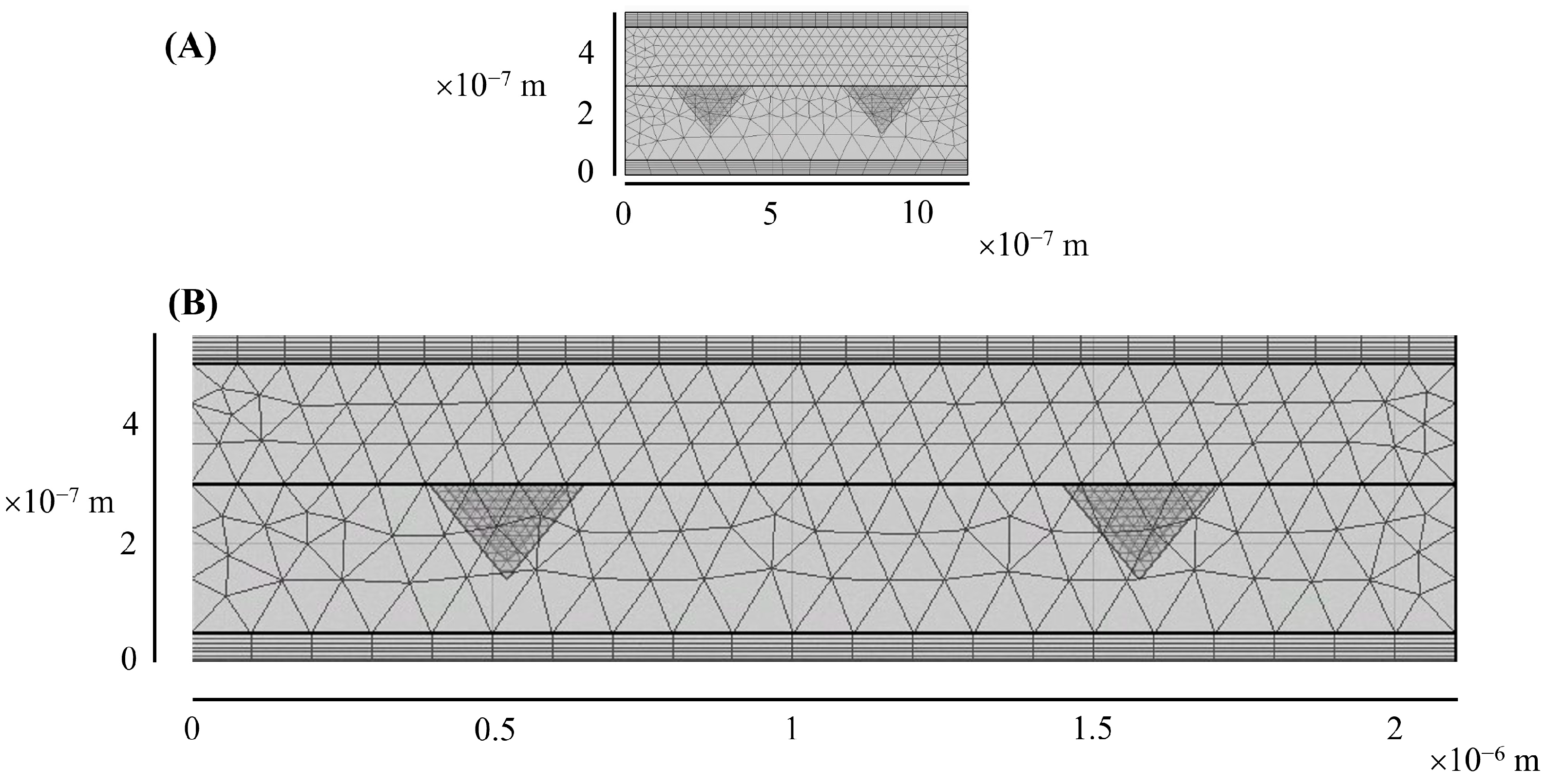
A fine mesh was utilized to accurately represent the physical system while maintaining computational efficiency. As illustrated in Figure 1, two structure spacings (3.2 μm and 7.9 μm) were modeled to investigate their influence on the distribution of their local electromagnetic fields. These design parameters were chosen to correspond with the physical dimensions of the fabricated substrates.
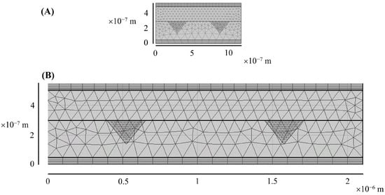
Figure 1.
Finite element mesh of the inverted-pyramid arrays with spacings of (A) 3.2 μm and (B) 7.9 μm.
A full-field, frequency-domain simulation was performed within the defined computational domain. Periodic boundary conditions were applied along the lateral boundaries to emulate an infinite metasurface array. To eliminate reflections and simulate an open boundary environment, perfectly matched layers (PMLs) with a thickness of 50 nm were implemented at the top and bottom boundaries. The excitation was introduced from the top of the domain using a linearly polarized plane wave. The material domains were defined as Au for the nanostructured layer, Si for the substrate, and air as the surrounding dielectric medium. The material properties were specified as follows: the Si substrate was modeled using the refractive index data reported by Jellison in the 0.234–0.840 μm wavelength range, and the Au nanostructure was defined using the optical constants for a 25 nm thick gold film, as reported by Yakubovsky over the 0.30–2.0 μm spectral range. Air was modeled with a refractive index of 1.0.
2.3. Raman Measurement
Prior to SERS analysis, the inverted-pyramidal Au array substrates were incubated in 4-MBA (1.0 mM) for 30 min, then rinsed with ultrapure water and dried in vacuum in a dark atmosphere for 1 hr at room temperature. Then, the Raman spectra were recorded using a confocal micro-Raman system with a 10 mW 780 nm laser (Thermo Scientific Inc., Waltham, MA, USA).
For Raman mapping analysis, 4-MBA was also employed as the Raman reporter molecule. Raman spectroscopy was carried out using a confocal micro-Raman spectrometer equipped with a 780 nm excitation laser and a 50× objective lens. The excitation power was set to 10 mW. Spectral data were acquired with an integration time of 1 s per point and averaged over 10 scans. Raman mapping was performed across a 26 × 27 μm2 area with a spatial resolution of 1 μm.
3. Results and Discussion
3.1. Electric Field of the Inverted-Pyramidal Au Array
The enhancement mechanisms of SERS are generally categorized into two types: electromagnetic enhancement and chemical enhancement [32]. Traditionally, noble metal nanostructures, such as Au and Ag, have been considered the primary contributors to SERS signal amplification due to the intense localized electromagnetic “hot spots” generated by plasmon resonance [33].
In a previous study, we employed a patterned silicon substrate coated with a few layers of MoS2, rather than conventional metallic nanostructures [27]. Experimental results revealed that the Raman signal intensity within the inverted pyramid micro-pits of the MoS2/patterned silicon substrate was approximately 274 times greater than that of a planar silicon substrate. This remarkable SERS performance can be attributed to a combination of enhancement mechanisms: (1) molecular confinement effect—the micrometer-scale inverted pyramid structures effectively confine analyte molecules (R6G), increasing their interaction with the substrate and enhancing local concentration; (2) electric field-directed aggregation—the application of a longitudinal electric field promotes the directed migration of R6G molecules into the micro-pits, mitigating random molecular distribution and enhancing signal uniformity and intensity; (3) chemical enhancement by MoS2—the two-dimensional layered structure of MoS2 offers a large surface area favorable for analyte adsorption. More importantly, MoS2 facilitates charge transfer between the substrate and the analyte, significantly boosting Raman signal intensity. Few-layer MoS2 tends to exhibit a direct band gap, which further enhances the charge transfer mechanism and improves overall SERS sensitivity.
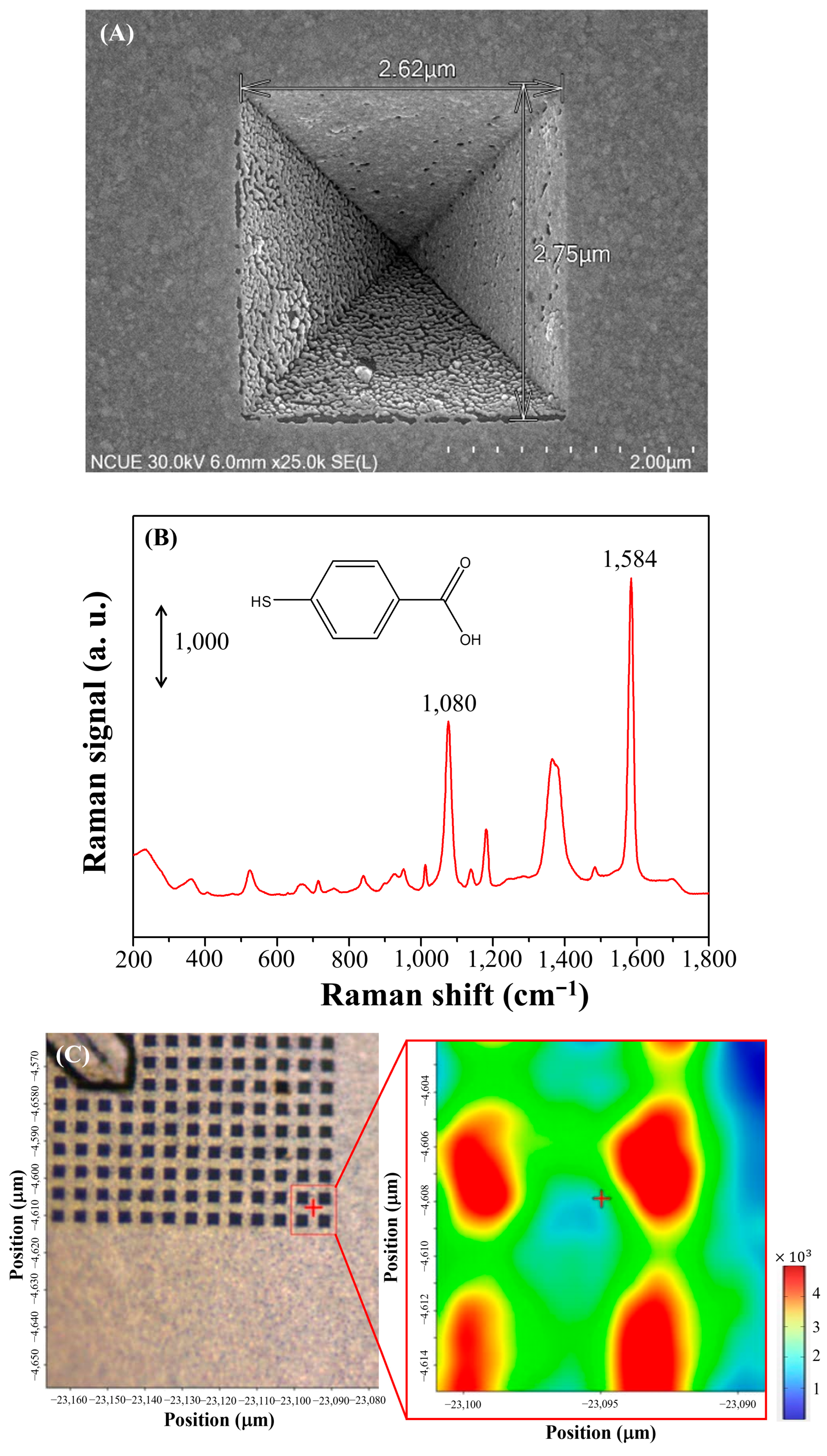
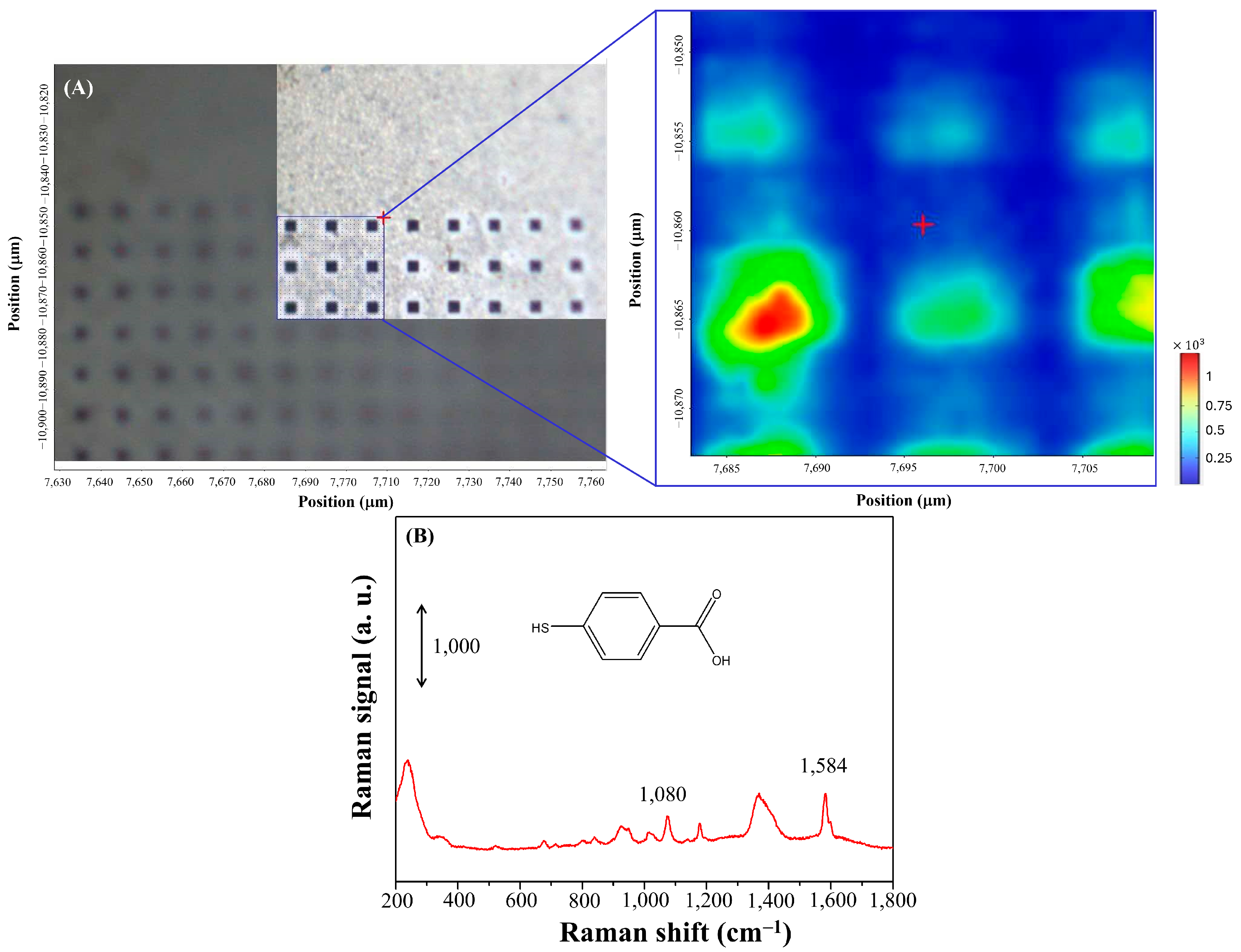
Figure 2A shows three-dimensional unit cell model of an inverted-pyramid gold array structure, as used in our previous study. The base of the rectangular pyramid measures 2.6 μm × 2.6 μm, with a depth of 1.6 μm. Herein, a Au layer, approximately 30 nm in thickness, was deposited onto the substrate using thermal evaporation. A 4-MBA molecule of 1.0 mM was used as a model molecule because of its large scattering cross-section and ability to form self-assembled monolayer on the surface of Au. Figure 2B shows the SERS spectrum of 4-MBA deposited on the inverted-pyramidal gold array substrate. Two stronger vibration bands of 4-MBA at approximately 1584 and 1080 cm−1 are assigned to the aromatic ring vibrations with C–S stretching characteristics v8a and v12, respectively [34]. The band at 1584 cm−1 was selected as a reference peak for Raman mapping in this study, and the resulting spatial distribution is presented in Figure 2C. Consistent with previous studies, the inverted-pyramidal gold array substrate demonstrates significantly enhanced Raman signal intensity, confirming its strong SERS performance.
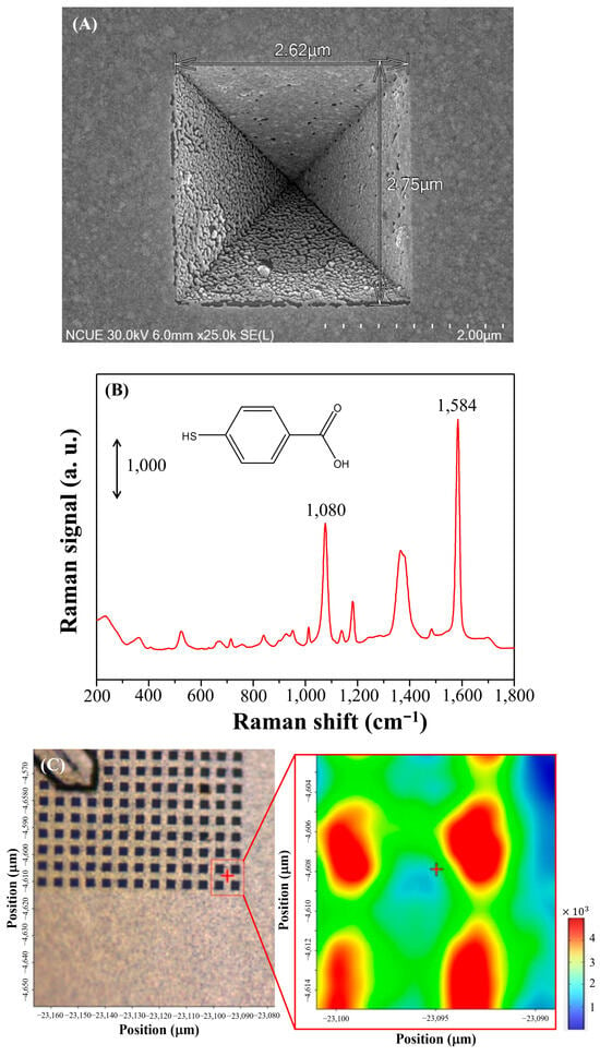
Figure 2.
(A) SEM image of the inverted-pyramidal Au structures, (B) Raman spectrum of 4-MBA using the inverted-pyramidal Au structure, and (C) photographic image using microscope and Raman mapping image of 4-MBA (Raman shift at 1584 cm−1) for the inverted-pyramidal Au array substrate with spacing of 5.9 μm.
However, we propose that the Raman enhancement mechanism observed in this study differs from that reported in our previous work. In the current experiment, 4-MBA molecules were adsorbed onto the Au-coated substrate via a simple incubation method, forming strong Au–S bonds. Under our experimental conditions, both the regions inside the inverted pyramidal structures and the areas between them were uniformly coated with Au, enabling potential chemical enhancement throughout the substrate. Nevertheless, a pronounced SERS signal was observed only within the inverted-pyramidal cavities. Unlike the prior study, no external electric field was applied to promote molecular accumulation within the pits, and due to the strong chemisorption between 4-MBA and Au, the previously proposed molecular confinement effect is unlikely to contribute here. These observations suggest that the dominant enhancement mechanism may arise from localized electromagnetic effects. Therefore, in this work, we employ numerical simulations to further investigate and elucidate the underlying factors responsible for the observed SERS signal enhancement within the inverted pyramidal structures.
3.2. Numerical Simulation of Electric Field Distribution of the Inverted-Pyramidal Au Array
It is also worth noting that sharp structures, such as Au or Ag nanospikes, are well-documented for generating strong electromagnetic field enhancements. Therefore, this study additionally aims to investigate, through theoretical simulations, whether localized electromagnetic field enhancement occurs at the edges or tips of the inverted-pyramid structures. If validated, this phenomenon could serve as a supplementary and impactful mechanism for further optimizing SERS substrate performance in future applications.
Figure 3 represents SEM images of the fabricated inverted-pyramidal Au array substrates. Figure 3A shows a periodic Au-coated inverted-pyramidal array with a center-to-center spacing of approximately 5.91 μm between adjacent structures. The side-to-side distances between neighboring pyramids are in the range of 3.21–3.33 μm. Figure 3B presents another array design, where the center-to-center distance between adjacent inverted-pyramidal structures is 10 μm. Correspondingly, the measured side-to-side distances are in the range of 7.84–7.94 μm. These structural measurements confirm the well-defined periodicity and uniformity of the fabricated inverted-pyramidal Au arrays.
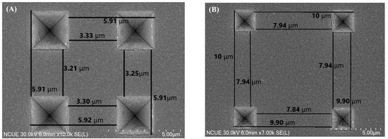
Figure 3.
SEM images of the inverted-pyramidal Au array substrates with spacings of (A) 5.9 μm and (B) 10 μm.
Therefore, to investigate the influence of structural spacing on electromagnetic field distribution, numerical simulations were conducted using the experimentally observed spacing distances. As shown in Figure 4, the simulated inter-pyramidal spacings ranged from 3.2 μm to 10 μm, corresponding to the measured variations in the fabricated substrates (Figure 3).

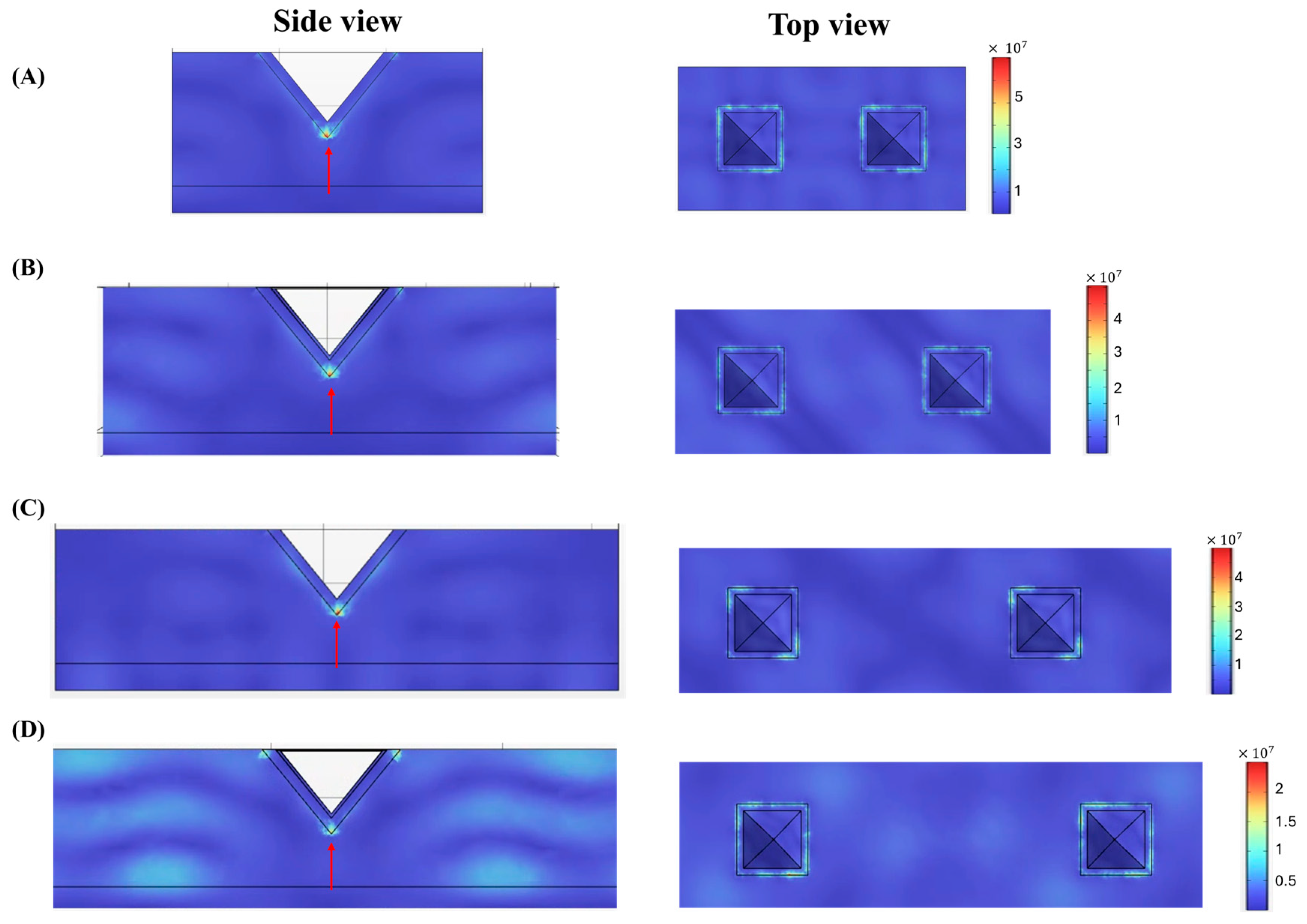
Figure 4.
Numerical simulation images (side view and top view) of the electric field distribution for the inverted-pyramidal Au array substrate with spacings of (A) 3.2 μm, (B) 5.5 μm, (C) 7.9 μm, and (D) 10 μm. The red arrows indicated the bottom rims of the structure exhibit strong electric fields.
Figure 4A demonstrated simulated spatial electric field distribution of the inter-pyramidal spacing at 3.2 μm in the x–z plane (side view) at the resonance wavelength of 780 nm under a laser excitation power of 10 mW. The results show that the highest plasmonic field intensity is concentrated at the tip of the inverted pyramid structure. Notably, the bottom rims of the structure exhibit strong electric fields, reaching up to 6.75 × 10⁷ V/m (as indicated by the red arrow). The top-view (x–y plane) electric field spectra reveal that the bottom left and right rims of the structure possess significantly higher field intensities (5.87 × 10⁷ V/m). This enhancement is attributed to the refractive index contrast between the substrate/Au thin film and the Au/air interface. Additionally, a slight penetration of the electric field into the silicon substrate is observed, likely due to the direct physical contact with the gold layer, contributing a baseline field from the substrate–metal interface.
The x–y plane simulation results shown in Figure 4B (the inter-pyramidal spacing at 5.5 μm) highlights that the maximum electric field is again localized at the tip of the inverted pyramid. The bottom edges of the structure exhibit a peak electric field intensity of 4.82 × 10⁷ V/m, while the top edges reach only 2.57 × 10⁷ V/m. This illustrates the high sensitivity of the localized electric field to changes in inter-structure spacing, particularly at the base region of the inverted pyramids. Figure 4C (the inter-pyramidal spacing at 7.9 μm) shows a similar trend, with the strongest field enhancement occurring at the tip of the inverted pyramidal structure. The bottom edges of the structure exhibit high electric field intensities up to 4.65 × 10⁷ V/m. The corresponding x–y plane simulation shows that the bottom rims consistently exhibit stronger electric fields than the top edges, which peak at 4.23 × 10⁷ V/m. In Figure 4D, the maximum electric field is again located at the tip of the inverted-pyramidal Au structure, reaching 1.92 × 10⁷ V/m. The x–y plane field distribution across the rectangular base shows markedly lower electric field intensities, with a peak value of 0.99 × 10⁷ V/m at the base, substantially lower than the field intensity observed at the tip.
3.3. Raman Images of the Inverted-Pyramidal Au Array Substrate
Figure 2C and Figure 5A also present Raman mapping results for inverted-pyramidal Au arrays with different inter-structure spacings, using the characteristic Raman shift of 4-MBA at 1584 cm−1. These results demonstrate a significant variation in Raman signal enhancement within individual inverted pyramids and regions between adjacent structures. The spatially uniform SERS intensity observed in Raman mapping (Figure 2C and Figure 5A) contrasts with the local electric field hotspots predicted by simulations (Figure 4). This discrepancy can be attributed to several reasons: (1) the spatial resolution of Raman mapping (~1 μm) may not be sufficient to resolve sub-micrometer hot spot gradients; (2) molecular adsorption and surface roughness may lead to a more distributed enhancement effect across the structure; and (3) photonic interactions between adjacent pyramids may induce broader field distributions than predicted by idealized models. Similar observations have been reported for Au nanostructures with gaps <100 nm, where the µm-scale laser spot masks the nanoscale field gradient [35]. In addition, the SEM images indeed suggest that the thermally evaporated Au layer forms a quasi-continuous film composed of densely packed, irregularly shaped nanoparticles, rather than a smooth conformal coating (Figure 2A). As a result, plasmonic nanogaps between adjacent nanoparticles can significantly contribute to SERS enhancement via localized gap-mode LSPR. While our FEM simulation model used a continuous 30 nm Au layer for simplification, we acknowledge that, in practice, these nanoscale gaps likely create additional hot spots not captured by the model. This effect complements the geometric enhancement from the inverted-pyramid structure. Thus, we proposed that the simulation represents an idealized geometry, whereas the actual enhancement results from both structural and particle-induced plasmonic effects.
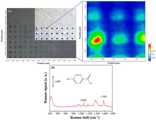
Figure 5.
(A) SEM image and Raman mapping image of 4-MBA (Raman shift at 1584 cm−1) and (B) Raman spectrum of 4-MBA for the inverted-pyramidal Au array substrates with spacing of 10 μm.
Furthermore, compared to the 5.9 µm spaced Au array shown in Figure 2C, the 10 µm spaced Au array (Figure 5A) exhibits reduced SERS uniformity. Hotspot uniformity is critical for sensor reproducibility. This phenomenon can be attributed to the following reasons: (1) the weaker inter-pyramidal plasmonic coupling at larger spacings, which diminishes both the intensity and localization of the electromagnetic field; (2) increased inter-structure distances create larger inactive regions between pyramids, resulting in a more uneven distribution of electromagnetic fields; (3) stochastic variations in nanoparticle deposition become more significant when fewer active structures fall within the laser excitation area, leading to inconsistent signal enhancement. In contrast, the 5.9 µm spaced array offers denser hot spot coverage and more uniform field overlap, resulting in both higher and more consistent SERS enhancement. These findings underscore the critical role of structural spacing optimization in the rational design of high-performance SERS substrates.
Figure 2B and Figure 5B show the Raman spectra of 4-MBA acquired at the center of inverted-pyramidal Au structures with inter-pyramidal spacings of 5.9 μm and 10 μm, respectively. The Raman signal intensity at 1584 cm−1 in Figure 2B was measured as 4125 ± 325 a.u., representing an approximately 3.99-fold enhancement compared to the intensity of 1033 ± 125 a.u., as shown in Figure 5B. This result highlights the significant influence of structural spacing on SERS performance. We demonstrated that reducing the inter-pyramidal distance further (e.g., to <3.2 μm) is expected to enhance plasmonic coupling between adjacent structures, potentially leading to even higher electromagnetic field intensities in the gap regions. However, achieving such tight spacing introduces significant manufacturing challenges that exceed our current laboratory resources, including issues such as etch merging, structural collapse, and non-uniform gold deposition. From a design standpoint, there exists an optimal spacing range that maximizes plasmonic coupling without compromising structural integrity. Subject to future funding and resource availability, we plan to investigate the feasibility of fabricating structures with sub-3 μm spacing and experimentally assess their effects. When the spacing between the inverted pyramids is larger, the influence of LSPR on the local electromagnetic field becomes less pronounced, leading to diminished SERS enhancement. This trend aligns with the electromagnetic field simulation results shown in Figure 6.
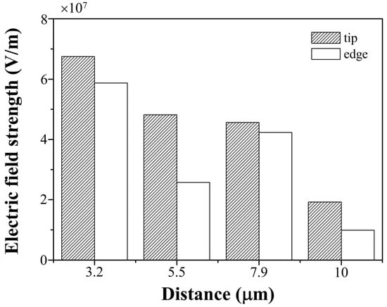
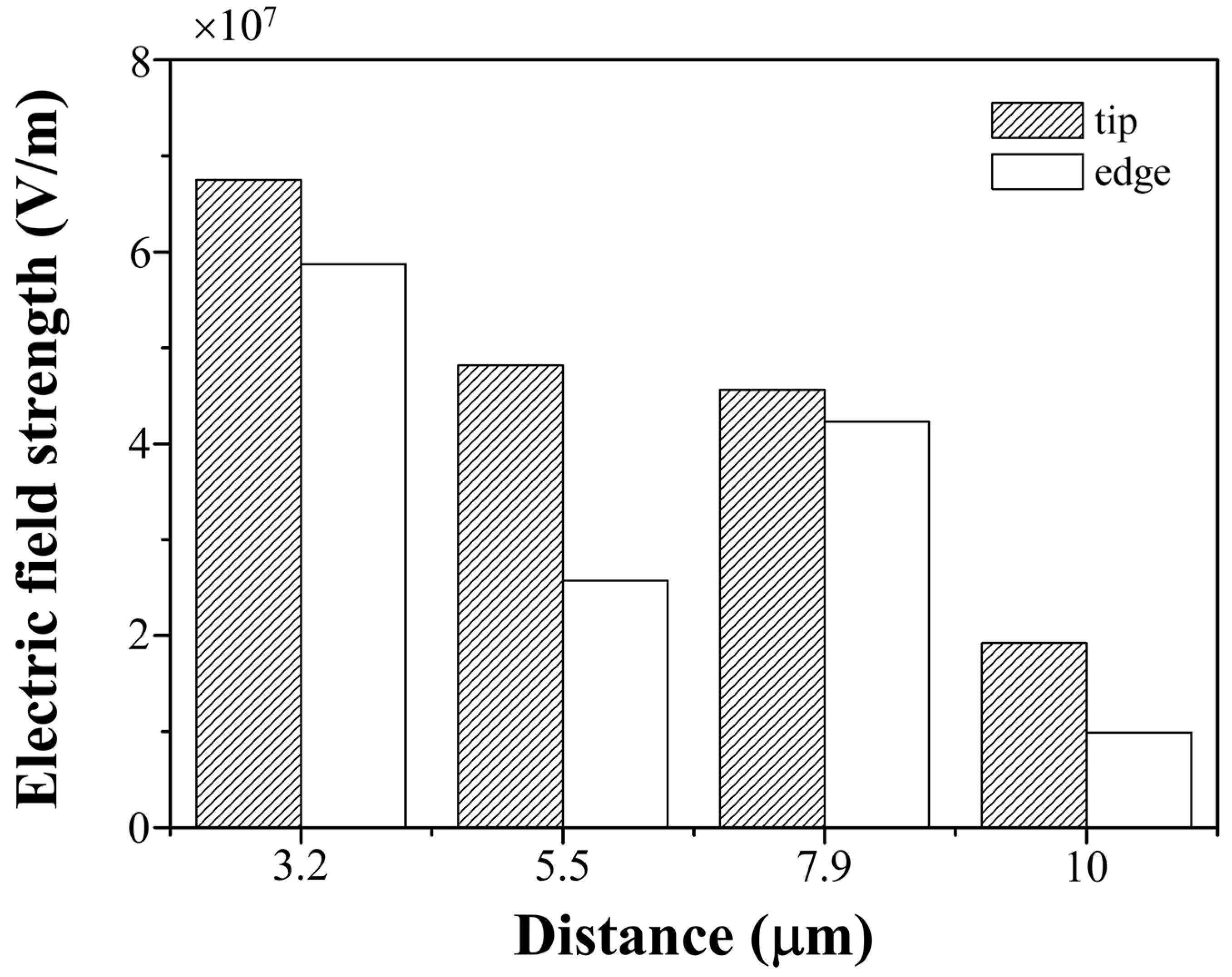
Figure 6.
The distance-dependent electric field strength for the inverted-pyramidal Au array substrates.
To further support this observation, we compiled the simulated electric field results for various inter-pyramidal distances, initially presented in Figure 4, into Figure 6. The simulations reveal that differences in distance significantly affect the electric field strength, particularly at the edges and tips of the inverted pyramids. As the distance increases from 3.2 μm to 10 μm, the electric field strength at the edge decreases from approximately 5.87 × 10⁷ V/m to 0.99 × 10⁷ V/m. Correspondingly, the electric field intensity at the pyramid tip also decreases, from 6.75 × 10⁷ V/m to 1.92 × 10⁷ V/m. While we did not directly calculate the absolute SERS enhancement factor (EF) in this work, a semi-quantitative relationship can be inferred. The local electric field enhancement (E) from simulation relates to SERS intensity enhancement as EF ∝ E4. Based on our simulation, the electric field intensity at the tip increased from 1.92 × 10⁷ V/m (for 10 µm spacing) to 4.82 × 10⁷ V/m (for 5.5 µm spacing), indicating an approximate 2.51-fold increase in field intensity, and potentially >39.7× increase in Raman signal by this estimation. Experimentally, we observed a ~3.99-fold increase in Raman intensity under the same spacing conditions. The disparity between simulated and observed enhancements can be attributed to averaging ensemble measurements and experimental imperfections such as molecular orientation and surface roughness. Nevertheless, the trend strongly supports the correlation between electromagnetic simulation and SERS performance.
These findings suggest that inter-structure spacing is critical in modulating edge and tip field enhancements in plasmonic metasurfaces [36]. In such systems, electromagnetic coupling between closely spaced structures can amplify fields through edge-to-edge plasmonic interactions [37]. This coupling enhances the field within the gap region and redistributes charges, modifying the overall field profile, including at the tip, due to changes in boundary conditions and mutual inductive effects [38,39]. Several factors, including geometry, dielectric environment, and the relative positioning of neighboring features, influence the extent of field enhancement. Consequently, the tip field is indirectly modulated by the edge field strength, which depends on the inter-pyramidal spacing. This phenomenon is well-documented in numerical studies in this study.
We further conducted a sensitivity test by varying the Au layer thickness from 20 nm to 40 nm in additional simulations (Table 2). Our simulations reveal that, across all examined inter-pyramidal spacings, a 30 nm Au layer consistently yields the highest electric field intensity at the base of the inverted pyramidal structures. For instance, at 3.2 μm spacing, increasing the Au thickness from 20 nm to 30 nm enhances the electric field from 5.88 × 10⁷ V/m to 6.75 × 10⁷ V/m, representing an approximate 12.9% increase. However, further increasing the thickness to 40 nm results in a significant decrease in field intensity to 3.04 × 10⁷ V/m, a reduction of about 55% compared to the 30 nm layer. This trend is consistent across larger inter-pyramidal spacings. At a 10 μm spacing, the field intensity drops from 1.92 × 10⁷ V/m at 30 nm thickness to 4.21 × 10⁶ V/m at 40 nm, marking a decrease of approximately 78.1%. These observations suggest that while a 30 nm Au layer optimally balances plasmonic activity and field confinement, thicker layers may suppress plasmon resonance due to increased optical losses and reduced field confinement. Therefore, precise control over the Au deposition process is important to ensure consistent and optimal SERS performance.
Table 2.
Simulated electric field strength at the tip of the inverted pyramid structure under different inter-pyramidal spacing and Au thickness.
4. Conclusions
In this study, we investigated how inter-pyramidal spacing affects localized electromagnetic field enhancement in inverted-pyramidal Au array substrates, using numerical simulations and Raman spectroscopy. Our simulation results showed that the electric field intensity at the tips and edges of the pyramidal structures is highly sensitive to the spacing between them; closer arrangements lead to significantly stronger field enhancements. Experimental Raman mapping using 4-MBA further supported these findings by demonstrating enhanced signal intensities in substrates with narrower spacings. The results highlight the importance of geometric parameters, particularly tip sharpness, inter-structure spacing and Au thickness, in modulating plasmonic field distribution. In contrast to our previous research on MoS2-based systems, where molecular confinement and electric field-assisted accumulation were key factors, the current Au-based structures primarily rely on electromagnetic enhancement driven by LSPR and inter-structure plasmonic coupling. This work establishes design principles for engineering high-performance plasmonic substrates and offers valuable insights for the development of next-generation SERS sensors. In addition, we acknowledge that fabrication imperfections, such as variations in pyramid base width, height, and tip sharpness, can significantly influence SERS performance. Although a systematic evaluation of these geometric variations was not conducted in the current study due to time constraints and limited laboratory resources, we plan to perform a comparative analysis of ±10% process variations using both numerical simulations and experimental Raman measurements in future work.
Author Contributions
Conceptualization, Y.A., Y.-P.T., F.-L.H. and T.-S.K.; methodology, Y.A. and Y.-P.T.; software, Y.A. and Y.-P.T.; validation, Y.A. and H.C.; formal analysis, Y.A. and H.C.; investigation, Y.A. and H.C.; resources, F.-L.H. and Y.-W.L.; data curation, Y.A. and H.C.; writing—original draft preparation, Y.A., I.S. and Y.-W.L.; writing—review and editing, Y.A., I.S. and Y.-W.L.; visualization, Y.A., H.C. and Y.-W.L.; supervision, I.S. and Y.-W.L.; project administration, F.-L.H., T.-S.K. and Y.-W.L.; funding acquisition, Y.-W.L. All authors have read and agreed to the published version of the manuscript.
Funding
This research was funded by the Taiwan National Science and Technology Council (NSTC) under contracts (113-2113-M-018-001) and The APC was funded by NSTC.
Institutional Review Board Statement
Not applicable.
Informed Consent Statement
Not applicable.
Data Availability Statement
Data are contained within the article.
Acknowledgments
This study was supported by the Taiwan National Science and Technology Council (NSTC) under contracts (113-2113-M-018-001) and the Ministry of Education (MOE) under Taiwan Experience Education Program (TEEP112).
Conflicts of Interest
The authors declare no conflicts of interest.
References
- Patel, B.; Darji, P.; Fnu, P.I.J.; Nalla, S.; Khatri, V.; Parikh, S. A comprehensive review and insight into the latest advancements in nanotechnology. Biosci. Biotech. Res. Asia 2024, 21, 985–1000. [Google Scholar] [CrossRef]
- Kalashgrani, M.Y.; Mousavi, S.M.; Akmal, M.H.; Gholami, A.; Omidifar, N.; Chiang, W.H.; Althomali, R.H.; Lai, C.W.; Rahman, M.M. Gold fluorescence nanoparticles for enhanced SERS detection in biomedical sensor applications: Current trends and future directions. Chem. Record 2024, Early View, e202300303. [Google Scholar] [CrossRef]
- Veg, E.; Hashmi, K.; Raza, S.; Joshi, S.; Rahman Khan, A.; Khan, T. The role of nanomaterials in diagnosis and targeted drug delivery. Chem. Biodivers. 2025, 22, e202401581. [Google Scholar] [CrossRef] [PubMed]
- Ganesh, K.M.; Bhaskar, S.; Cheerala, V.S.K.; Battampara, P.; Reddy, R.; Neelakantan, S.C.; Reddy, N.; Ramamurthy, S.S. Review of gold nanoparticles in surface plasmon-coupled emission technology: Effect of shape, hollow nanostructures, nano-assembly, metal–dielectric and heterometallic nanohybrids. Nanomaterials 2024, 14, 111. [Google Scholar] [CrossRef]
- Ashrafi, T.M.S.; Mohanty, G. Surface plasmon resonance sensors: A critical review of recent advances, market analysis, and future directions. Plasmonics 2025, 1–21. [Google Scholar] [CrossRef]
- Mcoyi, M.P.; Mpofu, K.T.; Sekhwama, M.; Mthunzi-Kufa, P. Developments in localized surface plasmon resonance. Plasmonics 2024, 1–40. [Google Scholar] [CrossRef]
- Verma, S.; Pathak, A.K.; Rahman, B.A. Review of biosensors based on plasmonic-enhanced processes in the metallic and meta-material-supported nanostructures. Micromachines 2024, 15, 502. [Google Scholar] [CrossRef] [PubMed]
- Goel, R.; Chakraborty, S.; Awasthi, V.; Bhardwaj, V.; Dubey, S.K. Exploring the various aspects of surface enhanced Raman spectroscopy (SERS) with focus on the recent progress: SERS-active substrate, SERS-instrumentation, SERS-application. Sens. Actuator A-Phys. 2024, 376, 115555. [Google Scholar] [CrossRef]
- Philip, A.; Kumar, A.R. The performance enhancement of surface plasmon resonance optical sensors using nanomaterials: A review. Coord. Chem. Rev. 2022, 458, 214424. [Google Scholar] [CrossRef]
- Gedney, S. Introduction to the Finite-Difference Time-Domain (FDTD) Method for Electromagnetics; Springer Nature: Berlin/Heidelberg, Germany, 2022. [Google Scholar]
- Amirjani, A.; Sadrnezhaad, S.K. Computational electromagnetics in plasmonic nanostructures. J. Mater. Chem. C 2021, 9, 9791–9819. [Google Scholar] [CrossRef]
- Dieperink, M.; Skorikov, A.; Claes, N.; Bals, S.; Albrecht, W. Considerations for electromagnetic simulations for a quantitative correlation of optical spectroscopy and electron tomography of plasmonic nanoparticles. Nanophotonics 2024, 13, 4647–4665. [Google Scholar] [CrossRef]
- Zhang, W.; Peng, Y.; Lin, C.; Xu, M.; Zhao, S.; Masaki, T.; Yang, Y. Research progress and application of two-dimensional materials for surface-enhanced Raman scattering. Surf. Sci. Technol. 2024, 2, 14. [Google Scholar] [CrossRef]
- Gomez-Cruz, J.; Bdour, Y.; Stamplecoskie, K.; Escobedo, C. FDTD analysis of hotspot-enabling hybrid nanohole-nanoparticle structures for SERS detection. Biosensors 2022, 12, 128. [Google Scholar] [CrossRef]
- Tang, J.; Hao, J.; Li, Z.; Bai, J. Towards understanding hybrid influencing mechanisms of substrate microstructure on SERS effect. Appl. Surf. Sci. 2024, 660, 159974. [Google Scholar] [CrossRef]
- Xie, Y.; Xu, J.; Shao, D.; Liu, Y.; Qu, X.; Hu, S.; Dong, B. SERS-based local field enhancement in biosensing applications. Molecules 2024, 30, 105. [Google Scholar] [CrossRef]
- Dai, Y.; Yue, L.; Li, W.; Pang, L. Plasmon-enhanced Raman spectroscopy to estimate near-electric-field enhancement. Phys. Rev. A 2024, 109, 053516. [Google Scholar] [CrossRef]
- Liu, J.; Meng, Z.; Zhou, J. High electric field enhancement induced by modal coupling for a plasmonic dimer array on a metallic Film. Photonics 2024, 11, 183. [Google Scholar] [CrossRef]
- Lee, Y.-M.; Kim, S.-E.; Park, J.-E. Strong coupling in plasmonic metal nanoparticles. Nano Converg. 2023, 10, 34. [Google Scholar] [CrossRef]
- Wu, T.; Lin, Y.-W. Surface-enhanced Raman scattering active gold nanoparticle/nanohole arrays fabricated through electron beam lithography. Appl. Surf. Sci. 2018, 435, 1143–1149. [Google Scholar] [CrossRef]
- Mao, F.; Ngo, G.L.; Nguyen, C.T.; Ledoux-Rak, I.; Lai, N.D. Direct fabrication and characterization of gold nanohole arrays. Opt. Express 2021, 29, 29841–29856. [Google Scholar] [CrossRef] [PubMed]
- Alvarez-Puebla, R.A. Effects of the Excitation Wavelength on the SERS Spectrum. J. Phys. Chem. Lett. 2012, 3, 857–866. [Google Scholar] [CrossRef] [PubMed]
- McFarland, A.D.; Young, M.A.; Dieringer, J.A.; Van Duyne, R.P. Wavelength-scanned surface-enhanced Raman excitation spectroscopy. J. Phys. Chem. B 2005, 109, 11279–11285. [Google Scholar] [CrossRef] [PubMed]
- Shin, H.-J.; Yoo, J.; Park, E.; Song, E.H.; Nam, J.-M. Plasmonic nanogap probes for surface-enhanced Raman scattering-based bioimaging and analysis. J. Phys. Chem. C 2024, 128, 17815–17824. [Google Scholar] [CrossRef]
- Wang, H.; Liu, Y.; Rao, G.; Wang, Y.; Du, X.; Hu, A.; Hu, Y.; Gong, C.; Wang, X.; Xiong, J. Coupling enhancement mechanisms, materials, and strategies for surface-enhanced Raman scattering devices. Analyst 2021, 146, 5008–5032. [Google Scholar] [CrossRef]
- Itoh, T.; Yamamoto, Y.S. Between plasmonics and surface-enhanced resonant Raman spectroscopy: Toward single-molecule strong coupling at a hotspot. Nanoscale 2021, 13, 1566–1580. [Google Scholar] [CrossRef]
- Ko, T.-S.; Hsieh, H.-Y.; Lee, C.; Chen, S.-H.; Chen, W.-C.; Wang, W.-L.; Lin, Y.-W.; Wu, S. Electric field-enhanced SERS detection using MoS2-coated patterned Si substrate with micro-pyramid pits. Nanomaterials 2024, 14, 1852. [Google Scholar] [CrossRef]
- Sun, J.; Wang, Z.; Yang, L.; He, Y.; Liu, R.; Ran, W.; Wang, Z.; Shao, B. An improved multiple competitive immuno-SERS sensing platform and its application in rapid field chemical toxin screening. Toxics 2022, 10, 605. [Google Scholar] [CrossRef]
- Lee, H.; Kim, W.; Song, M.Y.; Kim, D.H.; Jung, H.S.; Kim, W.; Choi, S. One-stop plasmonic nanocube-excited SERS immunoassay platform of multiple cardiac biomarkers for rapid screening and progressive tracing of acute myocardial infarction. Small 2024, 20, 2304999. [Google Scholar] [CrossRef]
- Yang, S.J.; Lee, J.U.; Jeon, M.J.; Sim, S.J. Highly sensitive surface-enhanced Raman scattering-based immunosensor incorporating half antibody-fragment for quantitative detection of Alzheimer’s disease biomarker in blood. Anal. Chim. Acta 2022, 1195, 339445. [Google Scholar] [CrossRef]
- Augustyniak, M.; Usarek, Z. Finite element method applied in electromagnetic NDTE: A review. J. Nondestruct. Eval. 2016, 35, 39. [Google Scholar] [CrossRef]
- Mohaghegh, F.; Tehrani, A.M.; Materny, A. Investigation of the importance of the electronic enhancement mechanism for surface-enhanced Raman scattering (SERS). J. Phys. Chem. C 2021, 125, 5158–5166. [Google Scholar] [CrossRef]
- Khurana, K.; Jaggi, N. Localized surface plasmonic properties of Au and Ag nanoparticles for sensors: A review. Plasmonics 2021, 16, 981–999. [Google Scholar] [CrossRef]
- Mhlanga, N.; Ntho, T.A. A theoretical study of 4-mercaptobenzoic acid assembled on Ag for surface-enhanced Raman scattering applications. Mater. Today Commun. 2021, 26, 101698. [Google Scholar] [CrossRef]
- Suganami, Y.; Oshikiri, T.; Mitomo, H.; Sasaki, K.; Liu, Y.E.; Shi, X.; Matsuo, Y.; Ijiro, K.; Misawa, H. Spatially uniform and quantitative surface-enhanced raman scattering under modal ultrastrong coupling beyond nanostructure homogeneity limits. ACS Nano 2024, 18, 4993–5002. [Google Scholar] [CrossRef] [PubMed]
- Grzeskiewicz, B.; Ptaszynski, K.; Kotkowiak, M. Near and far-field properties of nanoprisms with rounded edges. Plasmonics 2014, 9, 607–614. [Google Scholar] [CrossRef]
- Magdy, M. A conceptual overview of surface-enhanced Raman scattering (SERS). Plasmonics 2023, 18, 803–809. [Google Scholar] [CrossRef]
- Zhu, L.; Meng, Z.; Hu, S.; Zhao, T.; Zhao, B. Understanding metal–semiconductor plasmonic resonance coupling through surface-enhanced Raman scattering. ACS Appl. Mater. Interfaces 2023, 15, 22730–22736. [Google Scholar] [CrossRef]
- Xia, M.; Zhang, P.; Qiao, K.; Bai, Y.; Xie, Y.-H. Coupling SPP with LSPR for enhanced field confinement: A simulation study. J. Phys. Chem. C 2015, 120, 527–533. [Google Scholar] [CrossRef]

Disclaimer/Publisher’s Note: The statements, opinions and data contained in all publications are solely those of the individual author(s) and contributor(s) and not of MDPI and/or the editor(s). MDPI and/or the editor(s) disclaim responsibility for any injury to people or property resulting from any ideas, methods, instructions or products referred to in the content. |
© 2025 by the authors. Licensee MDPI, Basel, Switzerland. This article is an open access article distributed under the terms and conditions of the Creative Commons Attribution (CC BY) license (https://creativecommons.org/licenses/by/4.0/).