Abstract
The generation of hot electrons through non-radiative decay processes of surface plasmons (SPs) has been extensively demonstrated, enabling the preparation of high-performance hot-electron photodetectors without limitations imposed by material band gap widths. In this paper, a near-infrared wideband hot-electron metal semiconductor photodetector (WHEMSPD) is proposed based on a metal grating plasmonic structure, and its optical and electrical properties are numerically verified. This structure exhibits excellent broadband characteristics within the long-wave near-infrared range (LW-NIR) of 1200–1800 nm, achieving an absorption of approximately 0.7 between 1200 and 1700 nm, with a peak of 0.98 at 1400 nm. The metal grating structure can effectively enhance the excitation of plasmons on the surface and thus increase the absorption within a larger bandwidth. In terms of electrical performance, the responsivity of the WHEMSPD reaches over 20 mA/W within the wavelength range of 1200–1500 nm, with the peak responsivity reaching 28.3 mA/W around 1320 nm. WHEMSPDs in the LW-NIR can be widely used in military, remote sensing, communication, and other related fields.
1. Introduction
It is well known that the discovery of surface plasmon (SP) technology has provided more ideas for enhancing electromagnetic wave absorption, and it has improved the photoelectric performance of micro–nano optoelectronic devices [1]. SPs are known to decay non-radiatively into high-energy electrons [2]. Recent studies have shown that hot electrons can be used for many applications, including light detection [3,4], photovoltaic devices [5,6], photocatalysis [7,8], and surface imaging [9,10]. In terms of light detection, hot-electron devices generally form Schottky barriers through contact between metal surfaces and semiconductors. The hot electrons produced by the non-radiative decay of SPs can be transferred to the metal–semiconductor interface and injected into the conduction band of the semiconductor prior to thermalization, resulting in a photocurrent. In this case, the bandwidth of the photodetector is limited by the height of the Schottky barrier rather than the band gap of the semiconductor. This allows us to achieve broadband absorption at energies below the semiconductor band gap [11].
However, the main drawback of this class of hot-electron photodetectors is their low responsivity, typically between 10 and 100 μA/W [12]. This shortcoming can be overcome by controlling the geometry of the nanoantenna. For example, in 2011, M. Knight et al. proposed placing a nanostructure of a metal nanoantenna on a silicon substrate, allowing it to function as a light absorber and photodiode, which increased its responsiveness and internal quantum efficiency (IQE) to 0.6 mA/W and 0.2%, respectively. In 2014, K. Lin et al. developed a deep groove/thin metal (DTTM) active antenna nanostructure which utilizes surface plasmons. The three-dimensional Schottky interface on the DTTM surface and the large area on both vertical sides improved the near-field electric field intensity. The responsivity was two to three orders of magnitude higher than that of the above devices [13]. In 2016, A. Ahmadivand et al. reported a hot-electron detector consisting of gallium nitride and aluminum nanodisk clusters operating in the ultraviolet band. Its absorption at resonance wavelengths could reach about 95% and its responsiveness at optical intensities of 20 μW/mm2 could reach 20 A/W [14]. M. Hu et al. used titanium dioxide to wrap gold nanowires in order to achieve metal–semiconductor contact and achieved high broadband absorption of 75% in the band range of 400–1100 nm through numerical optimization [15]. In 2018, L. Wen et al. proposed a plasmonic nanostructure composed of gold films on random silicon nanopores which has optical properties of high broadband absorption and is accompanied by strong electric field localization, with a responsivity of about 1.5–13 mA/W in the wavelength range of 1100–1500 nm [16]. It has been proved that the silicon pyramid-shaped structure can focus light on a small region. B. Desiatov et al. realized metal layer deposition at the top of the pyramid, which enabled the device to achieve relatively good photoelectric performance by increasing the hot-electron generation rate and alleviating the electron momentum mismatch [17].
On the other hand, we can also use the high-absorption characteristics of a metamaterial perfect absorber to improve the responsiveness of the device. Metamaterials refer to artificial materials that have not been discovered in nature and possess certain special properties. They have some properties that cannot be achieved with conventional materials and can be used to make high-efficiency optoelectronic devices such as broadband absorbers and sensors [18,19,20]. In 2014, L. Wei et al. combined a metamaterial perfect absorber with a 3D Schottky junction based on the high-absorption characteristics of the metamaterial; thus, its maximum responsivity could reach 3.37 mA/W. From the above, it can be seen that good-light-absorption nanostructures are a necessary condition for high-performance hot-electron photodetectors.
In order to overcome the problem of narrowband absorption and low responsivity, a metal–semiconductor structure based on silicon-based metal grating is proposed in this paper. A wideband hot-electron metal semiconductor photodetector (WHEMSPD) is realized by designing a metal grating nanostructure. The device has good photoelectric performance (its specific parameters are in Table 1). The bandwidth range of this device is 1350–1500 nm, so the device can be said to have good high-bandwidth absorption, and its responsivity can reach more than 20 mA/W at 1200–1500 nm. Near 1400 nm, the peak responsivity can reach 28.1 mA/W, with a maximum IQE of 3%.

Table 1.
WHEMSPD structure parameters (nm).
2. Models and Methods
The structure and parameters of the WHEMSPD are shown in Figure 1 and Table 1. The specific structure can be seen in Figure 1a,b. The WHEMSPD can be realized by lithography, and the method of covering the silicon substrate with a gold film layer can be realized by electron beam evaporation or the electrochemical method combined with electron beam lithography [21]. The silicon material adopted in this paper was n-silicon (n-Si). When Au comes into contact with n-Si, the Fermi energy levels of the two need to align to the same energy (thermal equilibrium), resulting in the bending of the energy band and the formation of an energy barrier. Electrons flow from n-Si to Au until the Fermi energy levels align, forming a Schottky barrier [22]. The theoretical value of the Schottky barrier (ΦBn) is obtained by subtracting the electron affinity (4.05 eV) of n-Si from the work function of gold (5.5 eV) (which is 1.45 eV) [23]. However, due to the Fermi-level pinning effect occurring during actual contact, its actual value will also be much lower than 1.45 eV. In this device, ΦBn is set at 0.54 eV [2].
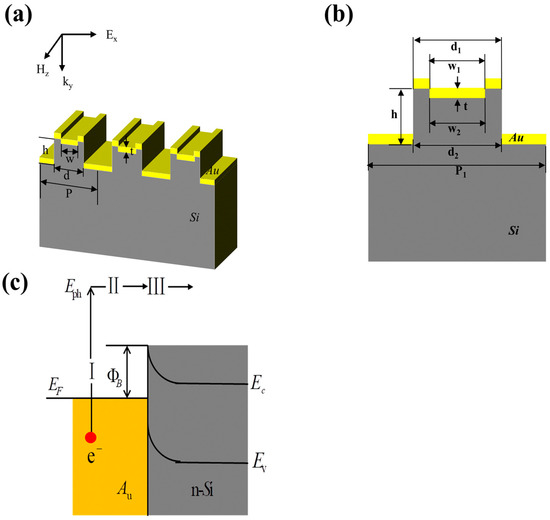
Figure 1.
(a) 3D structure diagram of WHEMSPD; (b) side view; (c) schematic diagram of hot-electron transfer.
In the optical modeling, we used COMSOL Multiphysics to simulate and analyze the optical performance of the WHEMSPD. The absorption of the photogenerated carrier can be described by the Maxwell equation, and the spatial distribution of the electromagnetic field can be obtained by the numerical solution of the Maxwell equation [24]. The two-dimensional structure was simulated using the wave optical module of COMSOL software version 6.1, the periodic boundary conditions were defined by using the Floquet boundary conditions in the x direction, and the scattering boundary conditions and a perfectly matched layer were set along the y direction. At the same time, the plane wave with TM polarization is vertically incident on the x-z side along the y direction. The absorption of the whole structure can be calculated by the ratio of total power density in volume V (Equation (2)) to the incident optical power (Equation (3)) [25].
where E is the electrical density, Ein is the incident electrical density, and ε″ is the imaginary part of the dielectric function. θ is the incident angle. ε0 is the vacuum dielectric constant and c0 is the speed of light.
The electrical formula utilized in this context is based on the hot-electron transfer mechanism illustrated in Figure 1c, which mainly comprises three sequential steps: 1. the generation of hot electrons through the non-radiative decay of surface plasmons on a femtosecond scale; 2. the migration of some hot electrons towards the metal–semiconductor interface; 3. the injection of hot electrons arriving at the interface into the semiconductor conduction band with a certain probability, provided that the energy of the incident photons exceeds the height of the Schottky barrier. Therefore, the electrical formula proposed by C. Scales et al. is used in this paper for numerical simulation analysis [26]. The key parameter calculation formulas employed in this electrical analysis include internal quantum efficiency (IQE,ηi), external quantum efficiency (EQE,ηe), responsivity (R), dark current density (Jd), and detectivity (D*) [26,27].
where ΦBn is the Schottky barrier of the gold–silicon interface (the measurement result is 0.54 eV [2]), h is the Planck constant, v is the photon frequency, A is the absorption of the plasmon structure, q is the unit charge, A** is the effective Richardson constant, T is the room temperature (300 K), and kB is the Boltzmann constant.
3. Results and Discussion
Figure 2a shows the absorption spectrum of a WHEMSPD with the simulated wavelength range from 1200 nm to 1800 nm in the LW-NIR [28]. The absorption of the WHEMSPD can reach more than 0.7 at 1500–1700 nm and the highest value of 0.98 at 1400 nm. In order to better demonstrate the photoelectric performance of the proposed WHEMSPD, we will compare the photoelectric parameters of a hot-electron metal semiconductor photodetector (HEMSPD) and the WHEMSPD. The HEMSPD has a peak responsivity of 27.7 mA/W, while also having broadband absorption characteristics. However, when its absorption is greater than 0.9, the band range is 1400–1500 nm and the absorption does not reach a larger value (close to 1), and the responsivity changes are unstable, which does not meet our expectations for high-broadband-absorption characteristics. Therefore, in order to further improve the photoelectric characteristics of the device, we proposed a WHEMSPD based on metal grating. The specific structural parameters of a HEMSPD are the same as those of the WHEMSPD, and the front view is inserted in Figure 3b,c. At the same time, we have put a three-dimensional structure diagram in the comparison diagram with the parameters, so that the reader can clearly see the difference between the two devices.
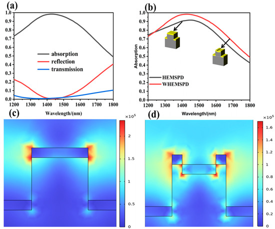
Figure 2.
(a) Optical properties of WHEMSPD; (b) absorption of WHEMSPD and HEMSPD; (c) electric field intensity distributions of HEMSPD at 1450 nm; (d) electric field intensity distributions of WHEMSPD at 1400 nm.
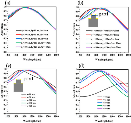
Figure 3.
(a) Different levels of absorption with ∆d; (b) different levels of absorption with ∆w; (c) different levels of absorption with w; (d) different levels of absorption with t.
The WHEMSPD has good broadband absorption characteristics in the wavelength range of 1200–1800 nm. And in the wavelength range of 1250–1800 nm, its absorption characteristics are higher than the HEMSPD.
In order to further analyze the optical characteristics of the WHEMSPD, we simulated the electric fields of the WHEMSPD and the HEMSPD at the resonance incident wavelength. It can be seen that, although both kinds of hot-electron photodetectors excite LSPs, not only can the WHEMSPD excite LSPs on the upper and lower resonators but its metal grating structure can also better stimulate LSPs [29]. Therefore, the device enhances the absorption effect in more positions, so that multiple absorptions can be superimposed in the same frequency band, conferring a higher absorption capacity. At the same time, the metal layer of this structure is also relatively thick. At the nanoscale, the increase in the gold layer thickness (t) within a certain range is conducive to the improvement of the absorption performance of the device [30], which is also the key reason for the high broadband absorption of the WHEMSPD.
Following this, we analyzed the influence of different structural parameters, ∆d = d1 − d2 and ∆w = w1 − w2, where w and t are the structural parameters of the device. Figure 3a analyzes the different degrees of sidewall slope during the preparation process by changing the ∆d of the silicon metal grating. However, it can be seen from Figure 3a that with the decrease in d1, the overall light absorption curve of the structure does not change much, which also indicates that the slope degree of the side wall does not have much influence on the actual preparation.
The purpose of changing ∆w is to simulate a situation in which part1 does not remain completely vertical during the actual sample preparation. We can see that the absorption of the device slightly decreases with the increase in ∆w in Figure 3b, and the absorption broadband of the device will narrow with the increase in ∆w, which is because the electric field strength near the metal grating of the device does not increase significantly with the increase in the ∆w value. Therefore, when we determine the value of ∆w, we need to try to ensure that the value of ∆w will not have a large impact on the absorption characteristics.
The width change of part1 can be seen in Figure 3c. When w is reduced to 80 nm, the absorption performance of the device is worse than that of the device with w ranging from 90 nm to 120 nm. When w changes from 90 nm to 120 nm, the absorption of the device only changes slightly, which has a small effect on the absorption performance of the entire device. In order to analyze the reasons for the decrease in absorption at w = 80 nm when the incident wavelength is greater than 1300 nm, the electric field mode diagrams at w = 100 nm and w = 80 nm at 1500 nm are placed in Figure 4a and Figure 4b, respectively. It can be seen that whether w is equal to 80 nm or 100 nm, the part of the device where the electric field changes greatly is located on the metal grating above part1, while the actual difference in the electric field intensity at other locations is not large.
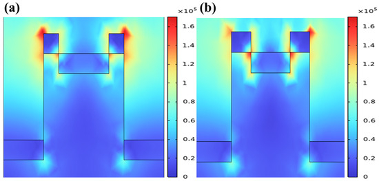
Figure 4.
(a) Electric field intensity distributions of WHEMSPD (w = 100 nm) at 1450 nm; (b) electric field intensity distributions of WHEMSPD (w = 80 nm) at 1450 nm.
Overall, the structural parameters of the metal grating have a great influence on the excitation of LSPs and the absorption performance. Therefore, we also need to ensure that the metal grating can maximize the excitation of LSPs.
As can be seen in Figure 3d, when the thickness of the gold layer increases from 10 nm to 20 nm, the absorption of the device is significantly redshifted, and the trend and value of the total absorption of the device become relatively stable at a thickness of 20–30 nm. Therefore, it can be concluded that when the thickness of the gold layer reaches an extreme value, its absorption performance changes relatively little. At the same time, for the WHEMSPD, a thicker gold layer will lead to a large loss of hot electrons, which will reduce the electrical performance of the device. Under this limitation, the thickness of the metal layer in the thin-layer WHEMSPD should be much less than the attenuation lengths of electrons and holes (where the attenuation lengths of electrons and holes are 74 nm and 55 nm, respectively [31,32]), so we compromised by combining the two different cases to obtain a value of w = 30 nm.
In addition to the influence of the device structure parameters, the angles of incident light also have a great influence on the metal grating structure. It can be seen in Figure 5 that when the incidence angle of a TM wave is less than 20°, there is only one absorption peak and the absorption value is basically unchanged, indicating that the absorption is relatively stable. When the incidence angle gradually approaches 80°, the single peak gradually becomes multiple peaks. This is because the horizontal vector of the wave will change when the incident light is incident at different incident angles, and the wave vector matching of the SP mode cannot be excited in each incident band, so the light absorption sensitive incident angle is greater than 20°.
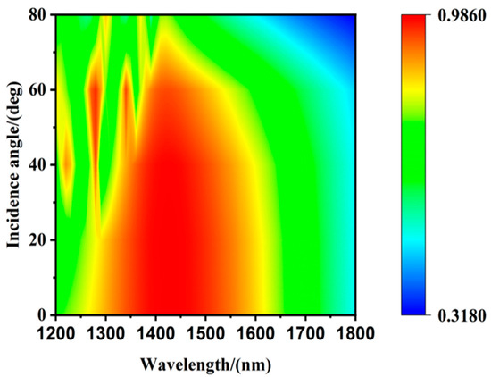
Figure 5.
The absorption under different incident angles.
4. Electrical Analysis
When light strikes the surface of the gold layer, the photons generate an electric current through the non-radiative decay process of surface plasmon generated by the metal surface [6,33]. We calculated the responsivity, IQE, EQE, dark current density, and detectivity under zero-bias voltage.
The two hot-electron photodetectors’ electrical characteristics are shown in Figure 6. Figure 6a,c compare their responsivity and detectivity. It can be seen that the responsivity of the WHEMSPD at 1300 nm reaches a maximum of 28.1 mA/W and the detectivity at 1300 nm also reaches an order of magnitude of about 20.3. Compared with the HEMSPD, the WHEMSPD has higher responsivity than the HEMSPD in the frequency band from 1240 nm to 1800 nm, and the responsivity at 1250–1350 nm can be almost stable at 28 mA/W and above. Figure 6b shows the EQE and IQE of the WHEMSPD. At the resonance wavelength, the IQE is equal to the EQE and is about 2.1%; that is, about two electron–hole pairs can be generated for every 100 photons absorbed. Therefore, it is obvious from the simulation that enhancing the absorption characteristics of the structure can significantly improve various electrical properties of the structure. However, due to the different photon energies corresponding to different spectra, the highest point of various electrical properties does not appear at the maximum absorption point.
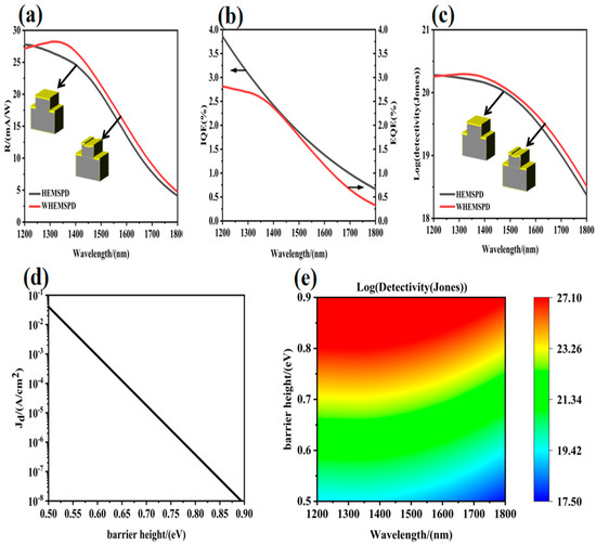
Figure 6.
(a) Comparison of responsivity between HEMSPD and WHEMSPD; (b) IQE and EQE of WHEMSPD; (c) comparison of detectability of HEMSPD and WHEMSPD; (d) dark current of WHEMSPD at different barrier heights; (e) detectability of WHEMSPD at different barrier heights and wavelengths.
In addition to the above parameters, the dark current density of the hot-electron photodetector is also a relatively important electrical performance parameter. Dark current refers to the current generated by the device itself in the absence of light, which exists in various circuits containing photosensitive devices [21]. We calculated the dark current density curve for when the barrier height changes from 0.5 eV to 0.9 eV, as shown in Figure 6d. It can be seen that the dark current density is always at a very low level (almost zero), so it can be ignored in the simulation process. Because detectability is used to describe the ability of a device to recognize weak optical signals in noise [21], the detectability of the device in the band of 0.5−0.9 eV is calculated in Figure 6e, and the results show that the value of the detectability of the device decreases with the increase in wavelength and the increase in wavelength height.
The fabrication process of the device in this paper is complicated, but the side wall of the silicon gate can be made inclined so that a gold layer can be attached to the surface. At the same time, because the gold resonators in the upper and lower layers are in a discrete state, it is also necessary to attach a gold layer of a certain thickness to the silicon side wall for connection, so as to form an electrical circuit. Although the thin gold layer will reduce the absorption performance, it helps with the conversion efficiency of the hot electrons.
In order to enable readers to have a further understanding of the photoelectric performance of the WHEMSPD proposed in this paper, the photoelectric performance of devices reported in other research is listed in Table 2 (where broadband with an absorption rate greater than 0.9 is listed), where a numerical comparison is made. In Table 2, we summarize the photoelectric performance parameters of hot-electron photodetectors with different structures in the literature, including theoretical values and actual measured values. It can be seen that the theoretical value of the photoelectric performance of the WHEMSPD proposed in this paper is relatively ideal compared with the theoretical values of other structures. It not only has good broadband absorption but also has relatively good electrical performance.
Finally, in order to enrich the research topic of this paper, common metal materials (Cu, Pd, Ag) were also selected as raw materials for metal gratings to carry out a photoelectric performance analysis [34,35]. It can be seen from Figure 7 that when the material of the metal grating is gold, the broadband photoelectric performance is the best in the near-infrared long-wave band. This is because the imaginary parts of the complex dielectric constants of these four materials are different [36,37] (the approximate comparison is Pd > Cu > Au > Ag), thereby affecting the absorption performance of the device. Although the absorption performance of Pd and Cu is relatively good among the four materials, the Au grating structure of the device at 1350–1800 nm can better excite surface plasmons, thus making the photoelectric performance of the Au grating superior to that of the Pd and Cu gratings. Meanwhile, Au itself has efficient inter-band transitions, a long hot-electron lifetime, and excellent interface characteristics in the near-infrared long-wave band, which are also the reasons why it is an ideal material for WHEMSPD metal gratings.
Table 2.
Performance comparison diagram of different devices.
Table 2.
Performance comparison diagram of different devices.
| Device Structure | Wavelength Range (A > 0.9) | R | D* | Ref. |
|---|---|---|---|---|
| WHEMSPD Au/Si | 1320–1550 nm | 28.3 mA/W@1320 nm | 6.51 × 10⁸ Jones | This work |
| HEMSPD Au/Si | 1400–1500 nm | 27.7 mA/W@1200 nm | 6.40 × 10⁸ Jones | This work |
| MetamaterialAu/Si | 1440–1540 nm | 3.37 mA/W@1470 nm (cal.) | N/A | [2] |
| Nanoislands Au/S | N/A | 3.5 mA/W@1200 nm | 8.74 × 10⁷ Jones (cal.) | [38] |
| Au grating/p-Si | N/A | 13 mA/W@1550 nm | 6.82 × 10⁶ Jones (cal.) | [39] |
| Au stripe/p-Si | N/A | 12 mA/W@1550 nm | 3.87 × 10⁶ Jones (cal.) | [40] |
| GaAs nanocone/MLG | N/A | 1.73 mA/W@850 nm | 1.83 × 10¹¹ Jones | [41] |
| Au asymmetric stripe/p-Si | N/A | 15.2 mA/W@1310 nm (cal.) | 1.17 × 10⁷ Jones (cal.) | [42] |
| Nanostructure VO2/MoS2 | 810–850 nm | 3.4 mA/W@820 nm | N/A | [43] |
| Nanopillar Au/Si | 0 | 2.5 mA/W@1310 nm | N/A | [44] |
| Double-cavity HEPD MoS2 | 780–800 nm/968–1008 nm | 23.6 mA/W@988 nm | N/A | [45] |
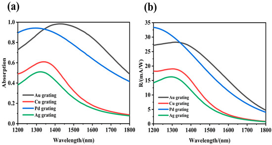
Figure 7.
(a) Absorption of metal gratings composed of different materials; (b) responsivity of metal gratings composed of different materials.
5. Conclusions
In this paper, we use the characteristic of multiple boundary angles to stimulate surface plasmon resonance on composite metal grating, so as to improve the absorption rate of the device. Due to the characteristics of the composite metal grating of the device, the widths of the top metal grating and the bottom metal grating are different, which also improves the photoelectric bandwidth performance of the device. At the same time, the influence on the absorption performance of the device is analyzed by comparing the absorption characteristics of the device under different structural parameters and different incident angles. Finally, through electrical analysis, it can be seen that the electrical performance of the WHEMSPD is closely related to the optical performance, so it is a feasible idea to improve the electrical performance by improving the optical performance of the device.
Author Contributions
Conceptualization, F.L.; Writing—original draft, H.H.; Writing—review & editing, Z.C., B.Z. and A.Z. All authors have read and agreed to the published version of the manuscript.
Funding
This work was supported by the Youth Science Foundation Project of the Natural Science Foundation of Tianjin (No. 18JCQNJC71400), the Key Project of the Tianjin Natural Science Foundation (No. 20JCZDJC00500), and the Youth Science Foundation Project of the National Natural Science Foundation of China (No. 61505144) (corresponding author: Fei Liu).
Institutional Review Board Statement
Not applicable.
Informed Consent Statement
Not applicable.
Data Availability Statement
All authors make sure that all data and materials, as well as software applications or custom code, support their published claims and comply with field standards.
Conflicts of Interest
The authors declare no conflicts of interest.
References
- Ai, Z.; Liu, H.; Cheng, S.; Zhang, H.; Yi, Z.; Zeng, Q.; Wu, P.; Zhang, J.; Tang, C.; Hao, Z. Four peak and high angle tilted insensitive surface plasmon resonance graphene absorber based on circular etching square window. J. Phys. D Appl. Phys. 2025, 58, 185305. [Google Scholar] [CrossRef]
- Li, W.; Valentine, J. Metamaterial perfect absorber based hot electron photodetection. Nano Lett. 2014, 14, 3510–3514. [Google Scholar] [CrossRef]
- Knight, M.W.; Sobhani, H.; Nordlander, P.; Halas, N.J. Photodetection with Active Optical Antennas. Science 2011, 332, 702–704. [Google Scholar] [CrossRef]
- Wang, F.; Melosh, N.A. Plasmonic Energy Collection through Hot Carrier Extraction. Nano Lett. 2011, 11, 5426–5430. [Google Scholar] [CrossRef]
- McFarland, E.W.; Tang, J. A photovoltaic device structure based on internal electron emission. Nature 2003, 421, 616–618. [Google Scholar] [CrossRef] [PubMed]
- Clavero, C. Plasmon-induced hot-electron generation at nanoparticle/metal-oxide interfaces for photovoltaic and photocatalytic devices. Nat. Photonics 2014, 8, 95–103. [Google Scholar] [CrossRef]
- Li, J.; Cushing, S.K.; Zheng, P.; Meng, F.; Chu, D.; Wu, N. Plasmon-induced photonic and energy-transfer enhancement of solar water splitting by a hematite nanorod array. Nat. Commun. 2013, 4, 2651. [Google Scholar] [CrossRef] [PubMed]
- Mubeen, S.; Lee, J.; Singh, N.; Kramer, S.; Stucky, G.D.; Moskovits, M. An autonomous photosynthetic device in which all charge carriers derive from surface plasmons. Nat. Nanotechnol. 2013, 8, 247–251. [Google Scholar] [CrossRef]
- Giugni, A.; Torre, B.; Toma, A.; Francardi, M.; Malerba, M.; Alabastri, A.; Zaccaria, R.P.; Stockman, M.I.; Di Fabrizio, E. Hot-electron nanoscopy using adiabatic compression of surface plasmons. Nat. Nanotechnol. 2013, 8, 845–852. [Google Scholar] [CrossRef]
- Schuck, P.J. Hot electrons go through the barrier. Nat. Nanotechnol. 2013, 8, 799–800. [Google Scholar] [CrossRef]
- Ueno, K.; Misawa, H. Plasmon-enhanced photocurrent generation and water oxidation from visible to near-infrared wave-lengths. NPG Asia Mater. 2013, 5, e61. [Google Scholar] [CrossRef]
- Knight, M.W.; Wang, Y.; Urban, A.S.; Sobhani, A.; Zheng, B.Y.; Nordlander, P.; Halas, N.J. Embedding Plasmonic Nanostructure Diodes Enhances Hot Electron Emission. Nano Lett. 2013, 13, 1687–1692. [Google Scholar] [CrossRef] [PubMed]
- Lin, K.T.; Chen, H.L.; Lai, Y.S.; Yu, C.C. Silicon-based broadband antenna for high responsivity and polarization-insensitive photodetection at telecommunication wavelengths. Nat. Commun. 2014, 5, 3288. [Google Scholar] [CrossRef]
- Ahmadivand, A.; Sinha, R.; Vabbina, P.K. Hot electron generation by aluminum oligomers in plasmonic ultraviolet photodetectors. Opt. Express 2016, 24, 13665–13678. [Google Scholar] [CrossRef]
- Hu, M.; Yang, L.; Dai, H.; He, S. Broadband absorption and efficient hot-carrier photovoltaic conversion based on sunlight-induced non-radiative decay of propagating surface plasmon polaritons. Sci. Rep. 2017, 7, 4809. [Google Scholar] [CrossRef]
- Wen, L.; Chen, Y.; Liang, L.; Chen, Q. Hot Electron Harvesting via Photoelectric Ejection and Photothermal Heat Relaxation in Hotspots-Enriched Plasmonic/Photonic Disordered Nanocomposites. ACS Photonics 2018, 5, 581. [Google Scholar] [CrossRef]
- Desiatov, B.; Goykhman, I.; Mazurski, N.; Shappir, J.; Khurgin, J.B.; Levy, A. Plasmonic enhanced silicon pyramids for internal photoemission Schottky detectors in the near-infrared regime. Optica 2015, 2, 335. [Google Scholar] [CrossRef]
- Li, Z.; Cheng, S.; Zhang, H.; Yang, W.; Yi, Z.; Yi, Y.; Wang, J.; Ahmad, S.; Raza, R. Ultrathin broadband terahertz metamaterial based on single-layer nested patterned graphene. Phys. Lett. A 2025, 534, 130262. [Google Scholar] [CrossRef]
- Zeng, Z.; Li, H.; Zhang, H.; Cheng, S.; Yi, Y.; Yi, Z.; Wang, J.; Zhang, J. Tunable ultra-sensitive four-band terahertz sensors based on Dirac semimetals. Photonics Nanostructures-Fundam. Appl. 2025, 63, 101347. [Google Scholar] [CrossRef]
- Cheng, S.; Li, W.; Zhang, H.; Akhtar, M.N.; Yi, Z.; Zeng, Q.; Ma, C.; Sun, T.; Wu, P.; Ahmad, S. High sensitivity five band tunable metamaterial absorption device based on block like Dirac semimetals. Opt. Commun. 2024, 569, 130816. [Google Scholar] [CrossRef]
- Sayed, S.Y.; Wang, F.; Malac, M. Heteroepitaxial Growth of Gold Nanostructures on Silicon by Galvanic Displacement. ACS Nano 2009, 3, 2809–2817. [Google Scholar] [CrossRef] [PubMed]
- Wen, X.H.; Jia, Y.; Yu, L.Y.; Shao, L.; Chen, H.; Xia, C.J.; Tang, L.I.; Shi, H.F. Silicon based hot electron short wave infrared detection technology (cover paper·invited). Infrared Laser Eng. 2024, 53, 9–30. [Google Scholar]
- Zhang, C.; Cao, G.; Wu, S.; Shao, W.; Giannini, V.; Maier, S.A.; Li, X. Thermodynamic loss mechanisms and strategies for efficient hot-electron photoconversion. Nano Energy 2019, 55, 164–172. [Google Scholar] [CrossRef]
- Tao, Z.; Zhou, D.; Yin, H.; Cai, B.; Huo, T.; Ma, J.; Di, Z.; Hu, N.; Yang, Z.; Su, Y. Graphene/GaAs heterojunction for highly sensitive self-powered Visible/NIR photodetectors. Mater. Sci. Semicond. Process. 2020, 111, 104989. [Google Scholar] [CrossRef]
- Chalabi, H.; Schoen, D.T.; Brongersma, M.L. Hot-electron photodetection with a plasmonic nanostripe antenna. Nano Lett. 2014, 14, 1374–1380. [Google Scholar] [CrossRef]
- Scales, C.; Berini, P. Thin-Film Schottky Barrier Photodetector Models. IEEE J. Quantum Electron. 2010, 46, 633–643. [Google Scholar] [CrossRef]
- Sun, Q.X.; Zhang, C.; Shao, W.J.; Li, X.F. Photodetection by Hot Electrons or Hot Holes: A Comparable Study on Physics and Performances. ACS Omega 2013, 4, 6020–6027. [Google Scholar] [CrossRef] [PubMed]
- Zhang, C.; Luo, Y.; Maier, S.A.; Li, X. Recent Progress and Future Opportunities for Hot Carrier Photodetectors: From Ultraviolet to Infrared Bands. Laser Photonics Rev. 2022, 16, 2100714. [Google Scholar] [CrossRef]
- Roh, S.; Chung, T.; Lee, B. Overview of the Characteristics of Micro- and Nano- Structured Surface Plasmon Resonance Sensors. Sensors 2011, 11, 1565–1588. [Google Scholar] [CrossRef]
- Sobhani, A.; Knight, M.W.; Wang, Y.; Zheng, B.; King, N.S.; Brown, L.V.; Fang, Z.; Nordlander, P.; Halas, N.J. Narrowband photodetection in the near-infrared with a plasmon-induced hot electron device. Nat. Commun. 2013, 4, 1643. [Google Scholar] [CrossRef]
- Crowell, C.R.; Spitzer, W.G.; Howarth, L.E.; LaBate, E.E. Attenuation length measurements of hot electrons in metal films. Phys. Rev. 1962, 127, 2006–2015. [Google Scholar] [CrossRef]
- Stuart, R.N.; Wooten, F.; Spicer, W.E. Mean free path of hot electrons and holes in metals. Phys. Rev. Lett. 1963, 10, 7–9. [Google Scholar] [CrossRef]
- Furube, A.; Du, L.; Hara, K. Ultrafast Plasmon-Induced Electron Transfer from Gold Nanodots into TiO2 Nanoparticles. J. Am. Chem. Soc. 2007, 129, 14852–14853. [Google Scholar] [CrossRef] [PubMed]
- Chen, L.; Mao, S.; Shen, Z.; Zhang, Q.Z.; Zhang, C.; Wang, P.; Belfiore, L.A.; Tang, J.G. Isolate Utilization of Plasmonic Hot Holes in Optoelectronic Enhancement for Copper Iodide (CuI): A Cross-Investigation by Confocal Kelvin Probe Force Microscopy. Adv. Opt. Mater. 2023, 11, 2300230. [Google Scholar] [CrossRef]
- Chen, L.; Mao, S.; Wang, P.; Yao, Z.; Du, Z.L.; Zhu, Z.J.; Belfiore, L.A.; Tang, J.G. Visible Light Driven Hot-Electron Injection by Pd Nanoparticles: Fast Response in Metal–Semiconductor Photodetection. Adv. Opt. Mater. 2021, 9, 2001505. [Google Scholar] [CrossRef]
- Johnson, P.B.; Christy, R.W. Optical Constants of the Noble Metals. Phys. Rev. B 1972, 6, 4370–4379. [Google Scholar] [CrossRef]
- Weaver, J.H. Optical properties of Rh, Pd, Ir, and Pt. Phys. Rev. B 1974, 9, 1782–1792. [Google Scholar] [CrossRef]
- Nazirzadeh, M.A.; Atar, F.B.; Turgut, B.B.; Okyay, A.K. Random sized plasmonic nanoantennas on Silicon for low-cost broad-band near-infrared photodetection. Sci. Rep. 2014, 4, 7103. [Google Scholar] [CrossRef]
- Alavirad, M.; Olivieri, A.; Roy, L.; Berini, P. High-responsivity sub-bandgap hot-hole plasmonic Schottky detector. Opt. Express 2016, 24, 22544–22554. [Google Scholar] [CrossRef]
- Othman, N.; Berini, P. Nanoscale Schottky contact surface plasmon “point detectors” for optical beam scanning applications. Appl. Opt. 2017, 56, 3329–3334. [Google Scholar] [CrossRef]
- Luo, L.; Chen, J.; Wang, M.; Hu, H.; Wu, C.; Li, Q.; Wang, L.; Huang, J.; Liang, F. Near-infrared light photovoltaic detector based on GaAs nanocone array/monolayer graphene Schottky junction. Adv. Funct. Mater. 2014, 24, 2794–2800. [Google Scholar] [CrossRef]
- Ali, A.; Berini, P. Schottky contact surface-plasmon detector integrated with an n asymmetric metal stripe waveguide. Appl. Phys. Lett. 2009, 95, 021104. [Google Scholar]
- Zhu, Y.; Yu, P.; Ashalley, E.; Liu, T.; Lin, F.; Ji, H.; Takahara, J.; Govorov, A.; Wang, Z. Planar hot-electron photodetector utilizing high refractive index MoS2 in Fabry–Pérot perfect absorber. Nanotechnology 2020, 31, 274001. [Google Scholar] [CrossRef] [PubMed]
- Yang, Z.; Du, K.; Wang, H.; Lu, F.; Pang, Y.; Wang, J.; Gan, X.; Zhang, W.; Mei, T.; Chua, S.J. Near-infrared photodetection with plasmon-induced hot electrons using silicon nanopillar array structure. Nanotechnology 2018, 30, 075204. [Google Scholar] [CrossRef]
- Daliran, N.; Hassanzadeh, A.; Hatef, A. Bimodal multilayer nanostructure based on vanadium dioxide phase transition: Absorber and hot electron photodetector. Appl. Phys. A-Mater. 2022, 352, 128. [Google Scholar] [CrossRef]
Disclaimer/Publisher’s Note: The statements, opinions and data contained in all publications are solely those of the individual author(s) and contributor(s) and not of MDPI and/or the editor(s). MDPI and/or the editor(s) disclaim responsibility for any injury to people or property resulting from any ideas, methods, instructions or products referred to in the content. |
© 2025 by the authors. Licensee MDPI, Basel, Switzerland. This article is an open access article distributed under the terms and conditions of the Creative Commons Attribution (CC BY) license (https://creativecommons.org/licenses/by/4.0/).