Article

Stepped Confocal Microlens Array Fabricated by Femtosecond Laser

1
School of Mechanical Engineering, Shanghai Jiao Tong University, Shanghai 200000, China
2
Laboratory of Laser and Medical Innovation Application (LLMIA), Gongli Hospital of Shanghai Pudong New Area, Shanghai 200000, China
*
Author to whom correspondence should be addressed.
Photonics 2025, 12(5), 494; https://doi.org/10.3390/photonics12050494
Submission received: 25 April 2025 / Revised: 11 May 2025 / Accepted: 12 May 2025 / Published: 16 May 2025

Abstract

Multi-focal microlens arrays provide notable advantages over mono-focal counterparts, such as multi-scale imaging capabilities and optical aberration correction. However, existing multi-focal microlens arrays fabricated on continuous surfaces are incapable of achieving confocal imaging. As a result, multiple focus adjustments are required to acquire comprehensive image data, thereby complicating system design and increasing operational duration. To overcome this limitation, a stepped confocal surface microlens array is proposed, capable of simultaneously capturing images with multiple depths of field, various field-of-view scales, and different resolutions—without the need for additional focus adjustments. A combination of femtosecond laser processing and chemical etching was employed to fabricate microlenses with varying curvatures on a stepped fused silica substrate, which was subsequently used as a mold. The final stepped confocal microlens array was replicated via polydimethylsiloxane (PDMS) molding. Preliminary experimental analyses were carried out to determine the relationship between processing parameters and the resulting focal lengths. By precisely controlling these parameters, the fabricated stepped confocal microlens array successfully enabled confocal imaging, allowing for the simultaneous acquisition of diverse image data. This microlens array shows great potential in advancing lightweight, integrated, and highly stable optical systems for applications in optical sensing, spatial positioning, and machine vision.

1. Introduction

Growing demand for miniaturization, lightweight design, integration, and intelligence in optical systems has spurred extensive research into microlens arrays (MLAs). An MLA consists of numerous microlenses, ranging in size from micrometers to millimeters, arranged in defined patterns to diffuse, focus, homogenize, and reshape incident light beams [1,2]. As a next-generation miniature optical component, MLAs have become core components in various optical systems. In optical communication, MLAs facilitate the processing and modulation of optical signals, enhancing optical coupling efficiency, expanding communication bandwidth, and improving transmission speed and stability. In imaging applications, including light-field cameras, MLAs serve as critical components by projecting light from various spatial positions onto individual microlenses, each coupled with a photosensitive element, thereby enabling the recording of two-dimensional positional and directional information of spatially distributed light. Due to their compact size, low weight, high integration, flexible design capabilities, and superior optical performance, MLAs are widely used in bionic compound eyes [3,4,5,6], optical communications [7,8], optical sensing [9,10], virtual reality [11], 3D imaging [12,13,14,15,16,17,18,19], laser guidance [20,21], projection displays [22,23], and photovoltaics [24,25].
Fueled by rising market demand and advances in micro/nanofabrication technologies, research has increasingly focused on the development of smaller, higher-performance microlens arrays. Multiple fabrication methods have been explored, including inkjet printing [26,27,28], screen printing [14,29], nanoimprinting [30,31], thermal reflow [32,33], and mold forming. Among these, mold forming is widely adopted in industrial production for its high reproducibility, cost-effectiveness, and excellent surface finish [34]. Techniques such as photolithography [35,36], ion beam etching [37], and diamond turning [38,39] are used to fabricate microlens array molds in hard materials, each with specific advantages and limitations. (1) Photolithography offers high precision and tunable morphologies, enabling direct fabrication of microlens arrays and their molds; however, it is limited to planar structures, involves costly equipment, and requires complex procedures. (2) Ion beam etching allows for the production of micro/nanostructures with high surface quality and fine features but suffers from low throughput and limited process stability. (3) Single-point diamond turning ensures high accuracy but necessitates extremely low feed rates when machining brittle substrates like glass, reducing process efficiency and hindering scalability.
In contrast to the aforementioned methods, femtosecond laser processing provides ultrashort pulses, high peak power, submicron resolution, and true 3D fabrication capabilities. It enables the fabrication of polymer microlenses and microlens arrays on hard, brittle substrates. When combined with chemical etching, this technique improves surface finish while ensuring fabrication throughput. Moreover, the optical properties of microlenses can be tailored by adjusting laser parameters. This approach offers high throughput, broad tunability, large-area compatibility, excellent consistency, and applicability across diverse materials, and has attracted substantial research interest [40,41,42,43,44,45]. For example, Bian et al. [46] employed a femtosecond laser-assisted micromachining technique with chemical etching on a 3D displacement platform to fabricate omnidirectional concave microlens arrays on curved substrates. These were then replicated as bionic compound eyes with controlled size, high uniformity, and minimal aberrations. Similarly, Zhou et al. [47] used femtosecond laser irradiation followed by wet etching to fabricate high-density microlens arrays on sulfur-based glass, achieving up to 2300 microlenses within a 1 mm2 area, with diameters tunable between 15 and 70 μm by controlling the laser power and etching time.
Multifocal microlens arrays exhibit several advantages over mono-focal designs, including multiple fields of view (FOVs), extended depth of field, and improved optical aberration correction [48]. However, conventional multifocal microlens arrays are typically fabricated on continuous surfaces, requiring sequential focal plane adjustments to obtain complete image information and lacking the ability for simultaneous confocal imaging. The focal length is a critical parameter in multifocal microlens imaging, directly influencing both the field of view and depth of field. Integrating multiple focal lengths into a single array enables simultaneous imaging at different depths and resolutions, which is particularly valuable in light-field imaging, biomedical sensing, and 3D projection. In this study, we propose a fabrication approach for producing microlens arrays with varying curvatures on stepped substrates. Using single-variable femtosecond laser experiments, the relationships among laser processing parameters, microlens focal length, and numerical aperture (NA) are investigated. Based on these findings, processing parameters are iteratively optimized, enabling the fabrication of a stepped confocal microlens array (SCMLA) tailored for multifocality. Finite element simulations are conducted to evaluate the SCMLA’s optical performance using experimental input parameters, confirming the feasibility of multifocal confocal surface imaging. The SCMLA allows for simultaneous multi-depth, multi-scale, and multi-resolution image acquisition without the need for repeated refocusing. This advancement enhances both optical performance and structural compactness, offering a streamlined solution for optical sensing, spatial imaging, and machine vision applications that demand lightweight, integrated, and cost-effective optical systems.

2. Experimental

2.1. Materials and Methods

In this method, polydimethylsiloxane (PDMS) is employed as the fabrication material for the stepped confocal microlens array (SCMLA). PDMS-based optical components exhibit high transmittance, low dispersion, minimal absorption, and low scattering. Fused silica is chosen as the reusable mold material due to its low thermal expansion coefficient, excellent chemical and thermal stability, and ease of etching.
When light passes through a lens, it refracts due to a change in the refractive index, thereby altering its direction of propagation. An object placed on one side of the lens is focused to form a clear image on the opposite side, such as on an image sensor, a focal plane, or a display screen. The operational principle of a conventional microlens array is illustrated in Figure 1a. All microlenses are arranged on a continuous surface, each having the same focal length, thereby enabling confocal imaging at a fixed focal plane. The working principle of a planar multifocal microlens array is depicted in Figure 1b. In this configuration, microlenses with different focal lengths facilitate imaging at various focal planes. However, simultaneous imaging is not possible, since the focal plane must be adjusted repeatedly to acquire individual images.
The operating principle of the SCMLA is illustrated in Figure 1c. By tuning the laser processing parameters, the curvature, focal length, and numerical aperture (NA) of the microlenses can be precisely controlled. This configuration enables simultaneous imaging at a single focal plane, eliminating the need for repeated focus adjustments. As a result, the SCMLA supports multi-depth-of-field, multi-scale field-of-view, and multi-resolution imaging, thereby enhancing system performance and imaging flexibility. The fabrication process of the SCMLA is outlined in Figure 1d. Initially, steps of varying heights are fabricated on the fused silica substrate using a CO2 laser, with precise control over power and scanning speed. Subsequently, a femtosecond laser beam is focused onto the surface to form arrays of micro-pits under varied laser parameters. During femtosecond laser irradiation, nonlinear absorption of laser energy by electrons in fused silica initiates avalanche ionization. Due to the ultrahigh peak intensity of femtosecond pulses, multiple photons can be simultaneously absorbed, promoting electron excitation and generating seed electrons. These seed electrons generate high-temperature, high-density plasma through collisional and avalanche ionization, resulting in photochemical modification of the material. Accompanying mechanisms, including molecular bond cleavage and Coulomb explosion, contribute to pit formation during material ablation and induce periodic ripple structures around the pits.
The energy consumption during free electron excitation leads to rapid laser energy attenuation along the propagation depth. The mathematical model describing these ultrafast ionization processes is given below:
n e t = α i I n e + P ( I )
In the equations, ne is the electron density, I is the laser intensity, αi is the impact ionization coefficient and P(I) represents the multiphoton ionization term.
Silica crystals have a tetrahedral structure composed of one silicon atom and four oxygen atoms, interconnected by covalent bonds. Due to nonlinear effects such as multiphoton absorption and avalanche ionization induced by femtosecond laser irradiation, the Si–O–Si bond angle decreases, disrupting the [SiO4] network structure and reducing the material’s chemical stability. As a result, the laser-modified portion of the material becomes more reactive with hydrofluoric acid (HF). The pits and surrounding periodic stripe structures increase the surface area exposed to the solution, significantly enhancing the etching rate of the modified region compared to the unmodified region. The etching process progressively transforms the pits into smooth, spherical microlenses. PDMS was then used to invert the mold of the etched fused silica, resulting in the production of a SCMLA. The chemical reaction between SiO2 and HF is represented by [34,36,37]:
  S i O 2 + 6 H F = H 2 S i F 6 + 2 H 2 O  
Considering the requirements for both etching efficiency and etching quality, a 20% hydrofluoric acid (HF) solution was selected for etching at room temperature. After etching, the samples were cleaned with anhydrous ethanol and deionized water for 10 min and then dried with nitrogen gas to ensure a clean and residue-free surface. PDMS and its curing agent were mixed at a 10:1 ratio and subsequently cured and molded under vacuum at 80 °C for 1 h.

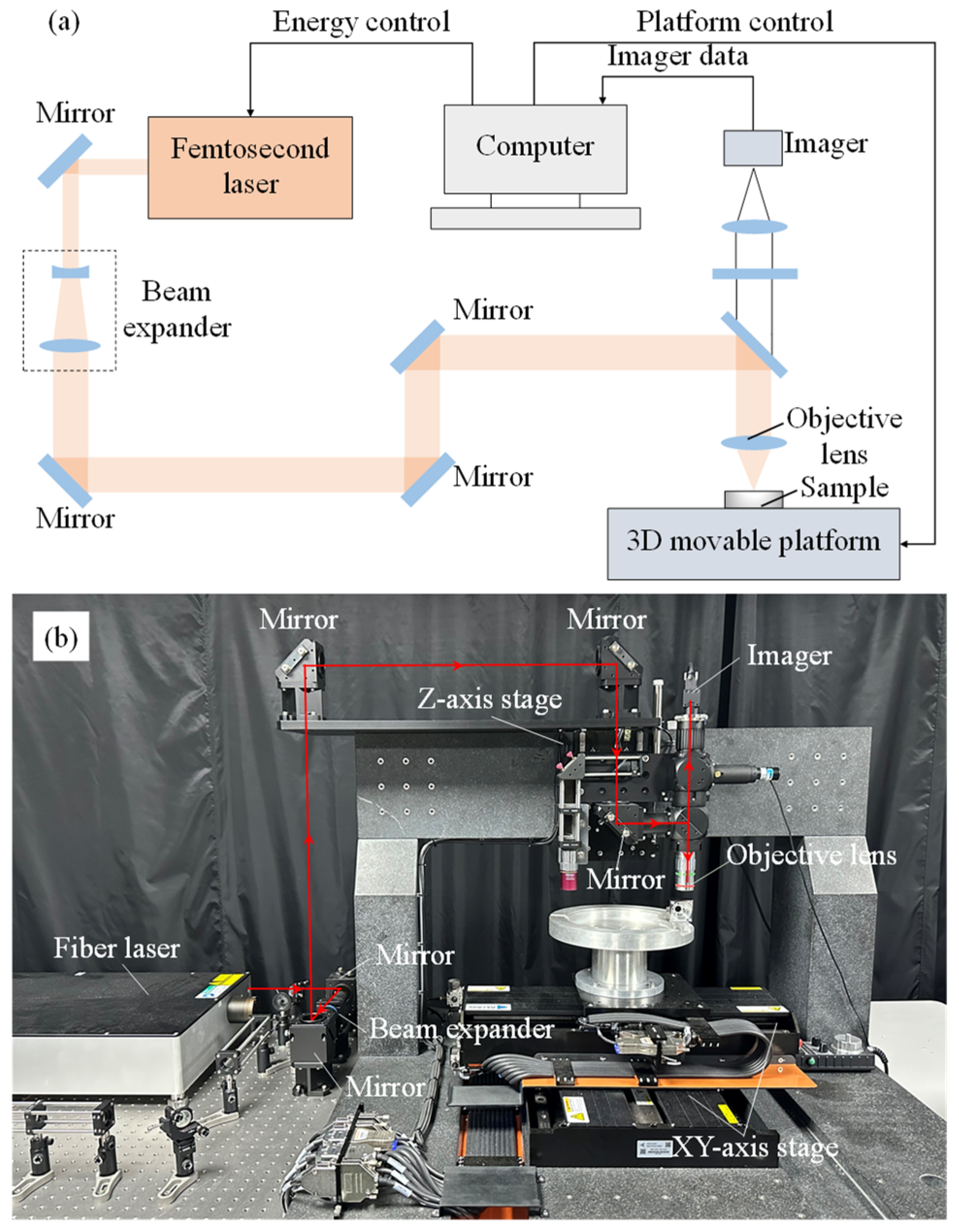
2.2. Experimental Setup

The femtosecond laser processing system used in this study is shown in Figure 2a. The main components include a femtosecond laser, beam expander, mirror sets, objective lens, charge-coupled device (CCD), and a three-axis precision displacement stage. The physical layout of the system is illustrated in Figure 2b. The femtosecond laser (FemtoYL-100) used for processing fused silica glass provides a maximum output power of 100 W, a wavelength of 1030 nm, and a pulse duration of 300 fs. The laser operates at a repetition rate of 25 kHz with a pulse-to-pulse stability of <1% RMS. The objective lens has a focal length (F) of 10 mm with an entrance aperture diameter (D0) of 8 mm and a numerical aperture (NA) of 0.4. The focal spot diameter (d) and focal depth (DOF) of the femtosecond laser can be theoretically calculated based on the following optical principles:
d = 4 λ F π D 0 1.65   μ m  
D O F = ± λ F 2 π D 0 2 ± 5.15   μ m
The beam expander regulates the laser spot size and incorporates multiple mirror sets to control the orientation of the optical path. The laser beam is subsequently focused onto the sample surface through an objective lens (20×, NA = 0.40, Mitutoyo, Kanagawa, Japan). A CCD aligned coaxially with the lens is installed for real-time observation and positioning. A three-axis precision displacement stage (Akribis, Singapore) was employed to carry the sample, offering a movement resolution of 20 nm and repeatability accuracy at the submicron level.

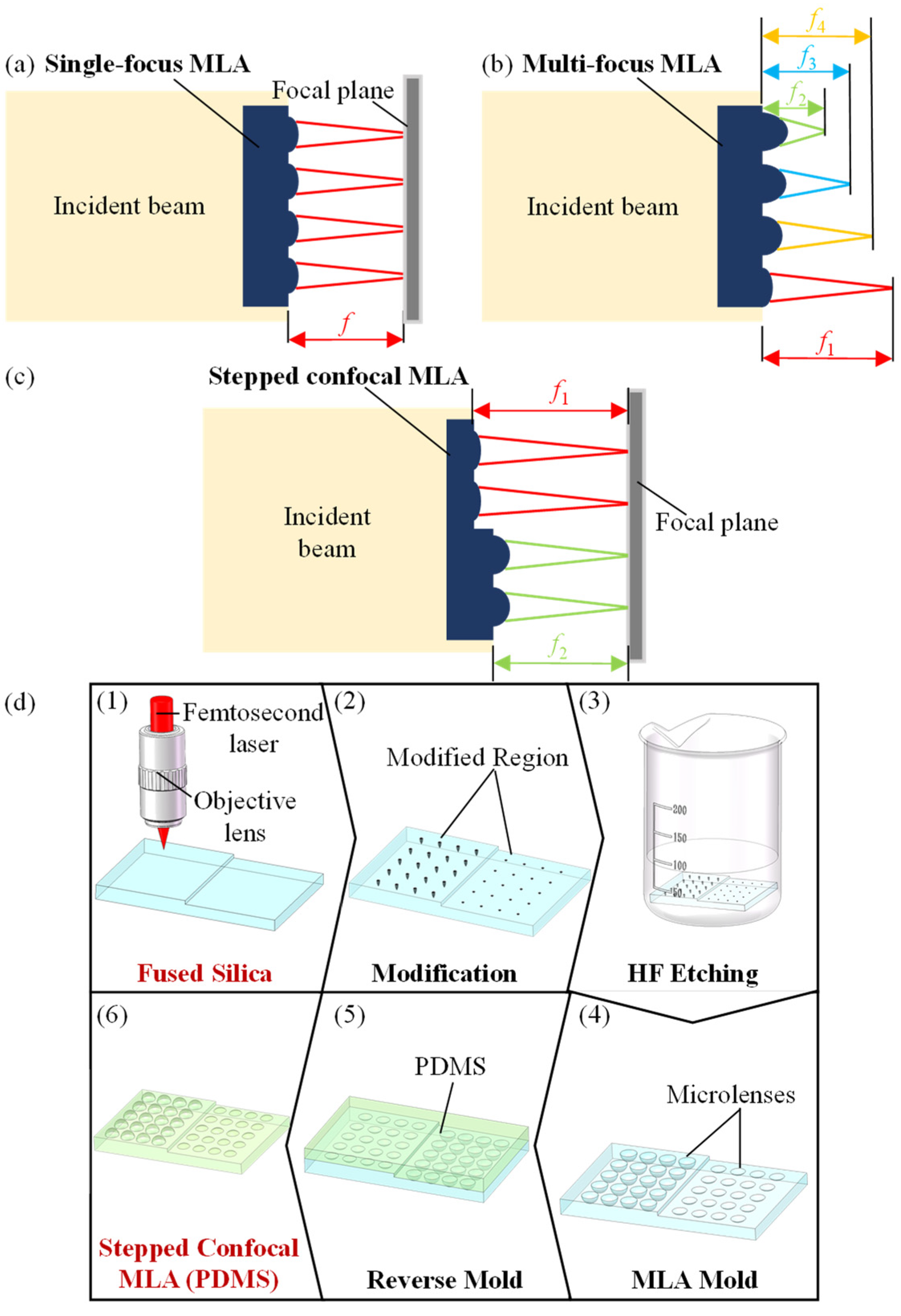
2.3. Fabrication of the SCMLA

To fabricate microlenses with controllable focal lengths, it is essential to characterize the final morphology of the microlens array after chemical etching. Figure 3a–c show the laser confocal morphology of microlenses after 20, 40, and 60 min of etching, respectively. As the etching time increases, both the microlens diameter and depth increase accordingly. Figure 3d presents a cross-sectional profile of a representative microlens. The blue line indicates the actual cross-sectional geometry, while the red dotted line represents the ideal spherical contour. The etched microlens array closely approximates a spherical surface. The focal length is subsequently calculated using the standard formula for a spherical lens.
The initial step in fabricating the SCMLA is to obtain microlenses with varying focal lengths. Therefore, the effects of laser pulse energy, number of pulses, focusing position, and etching time on the focal lengths of the microlenses must be investigated. The diameter (D) and depth (h) of each microlens were measured using a laser confocal microscope (VK-X3000, KEYENCE, Neu-Isenburg, Germany). The corresponding focal length and numerical aperture (NA) were then calculated using the following equations [34]:
R = h 2 + r 2 2 h
f = R n 1  
N A = r f
where R is the radius of curvature of the microlens; r (r = D/2) is the radius of the microlens; n is the refractive index of PDMS (n = 1.41); f is the focal length; and NA is the numerical aperture.
The formation mechanism of microlenses with varying focal lengths during the etching process is illustrated in Figure 4. Due to the PDMS inverted molding process, the height differences between steps, as discussed later, result from the inversion of the mold. Microlenses with lower step heights require longer focal lengths and larger curvature radii to enable stepped confocal imaging. Initially, the lower stepped pits are fabricated to be shallower by controlling the laser processing parameters, leading to correspondingly shallower modified regions. In contrast, the higher stepped pits are deeper, and their modified regions are accordingly deeper. As the etching rate of hydrofluoric acid for the laser-modified regions is significantly higher than for unmodified material, the etching process can be divided into three stages. In the first stage, both vertical and lateral etching occur within the modified regions. The modified material in the vertical direction of the lower step is completely removed, whereas a portion of the modified region in the lateral direction remains. In the higher step, parts of the modified regions in both the vertical and lateral directions persist. During the second stage, horizontal etching dominates for the lower step, expanding the pit diameter as the remaining modified material is removed. Simultaneously, the higher step continues to undergo both vertical and horizontal etching, further increasing the depth and diameter. In the third stage, once the modified regions are fully removed, the etching rates of the pit bottoms and the surrounding surface become equal. Vertical etching proceeds uniformly, while lateral etching continues, resulting in pits with increased diameter and nearly constant depth. The final microlens morphology is governed by the extent of the laser-modified regions, allowing the curvature and focal length to be precisely tuned by adjusting the processing parameters that define the modification extent.

2.4. Morphology Characterization

The microlens arrays’ 3D profile and depth data were characterized using a laser confocal scanning microscope (VK-X3000, KEYENCE, Neu-Isenburg, Germany). A surface profiler (KLA-Tencore D-120, Milpitas, CA, USA) was used to describe the step height and lens morphology. The top-view macroscopic morphology of the microlens array was examined using an optical microscope (MM-800L, Nikon, Tokyo, Japan).

3. Results and Discussion

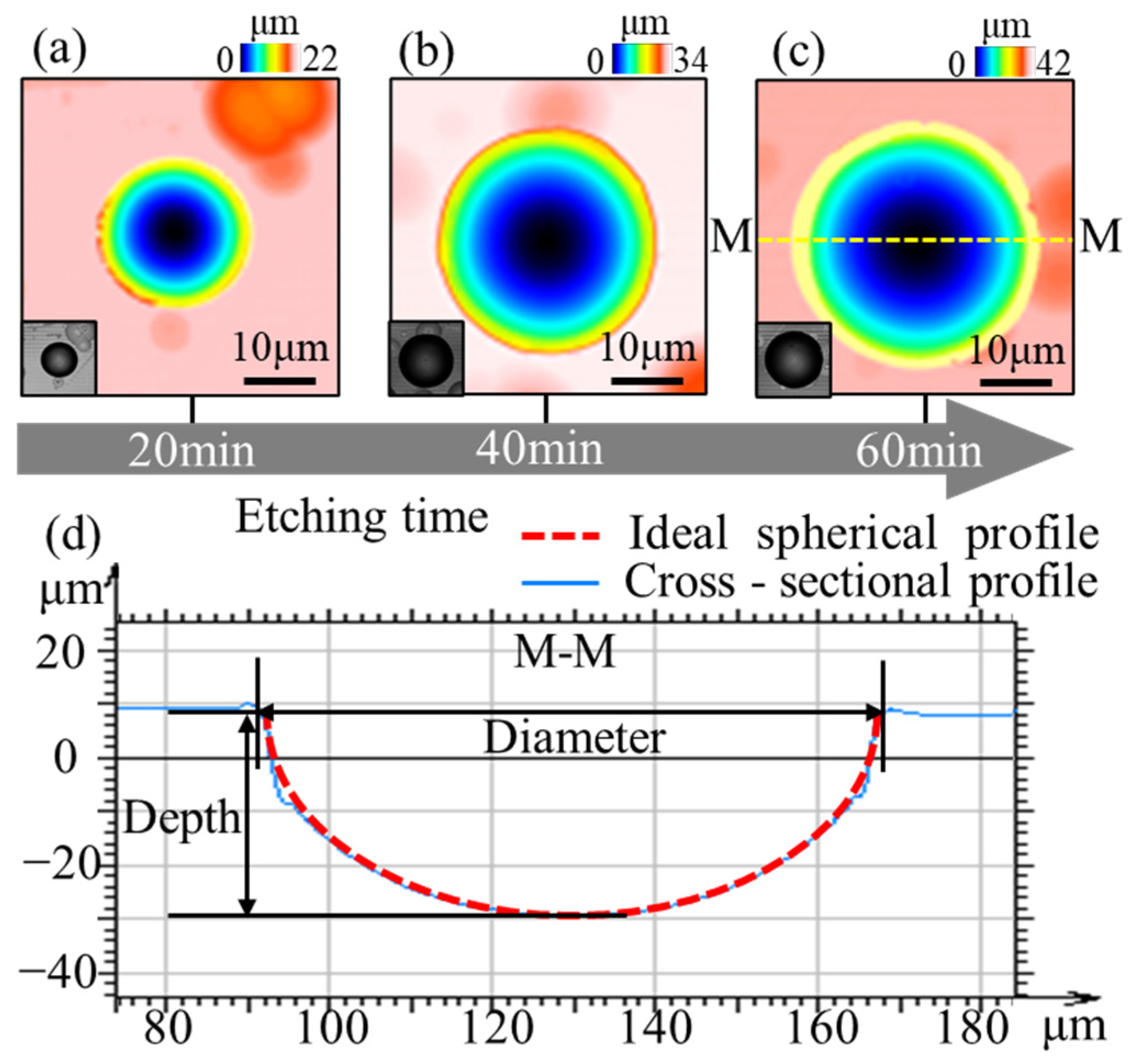
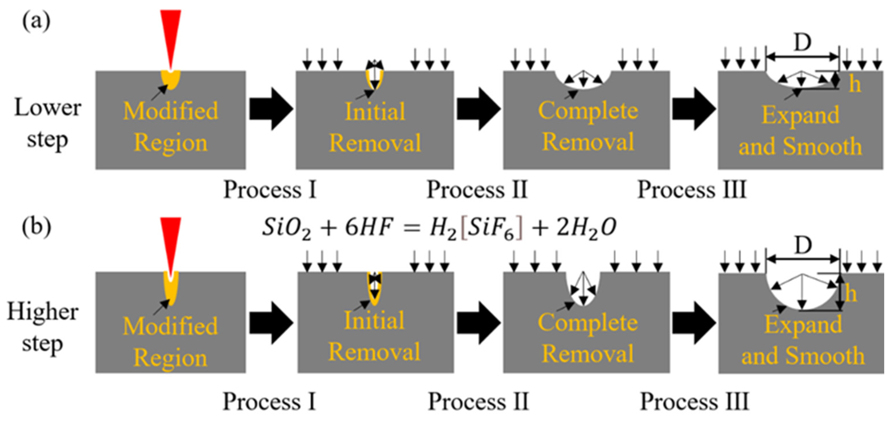
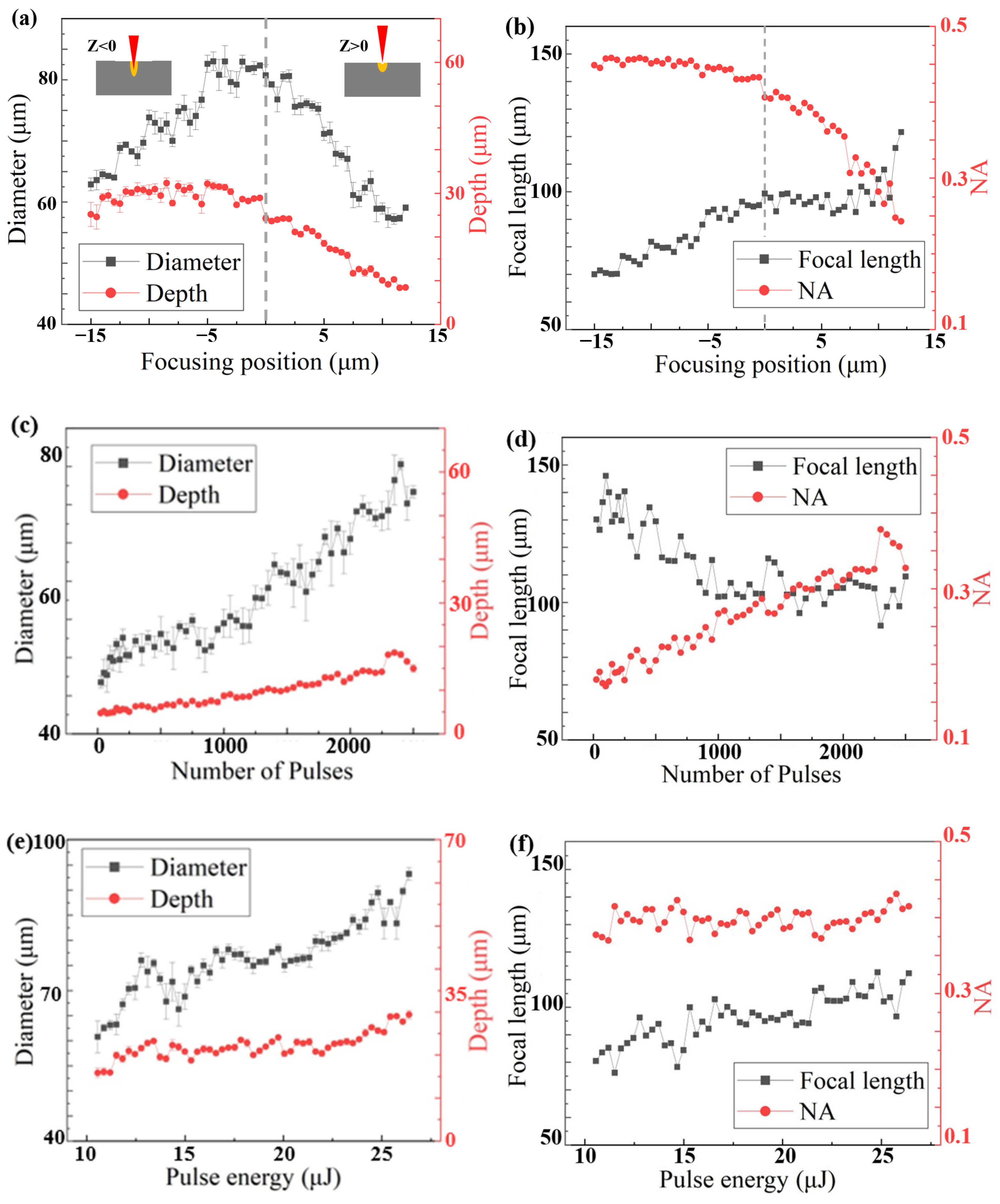
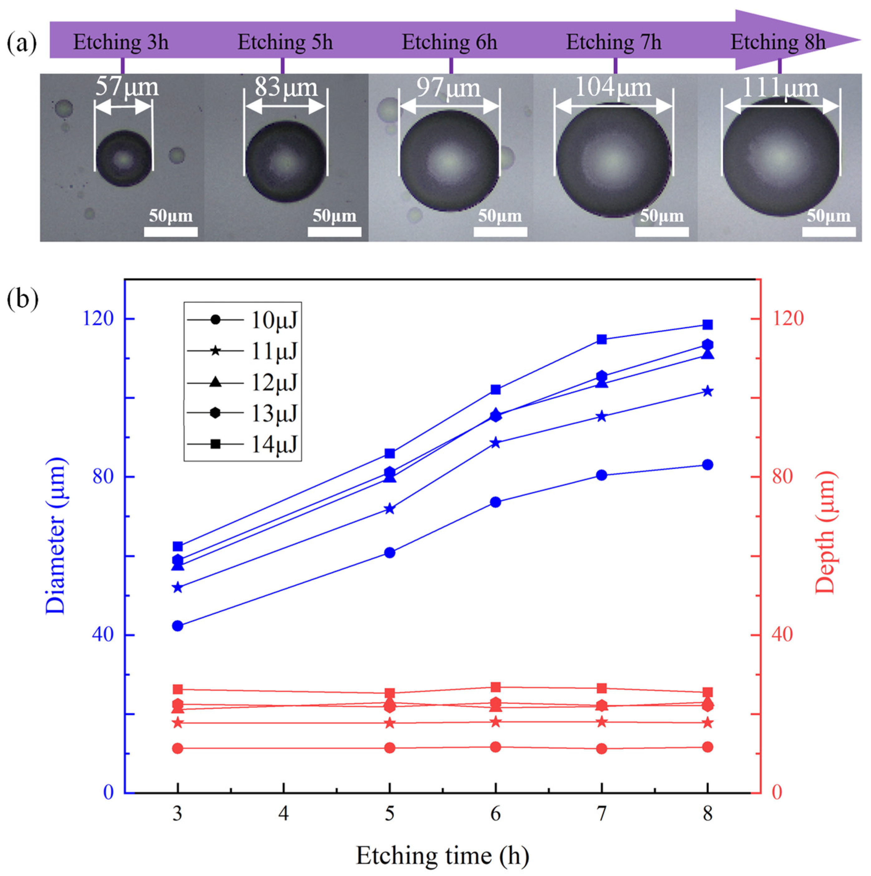
3.1. Morphology Control of Microlenses
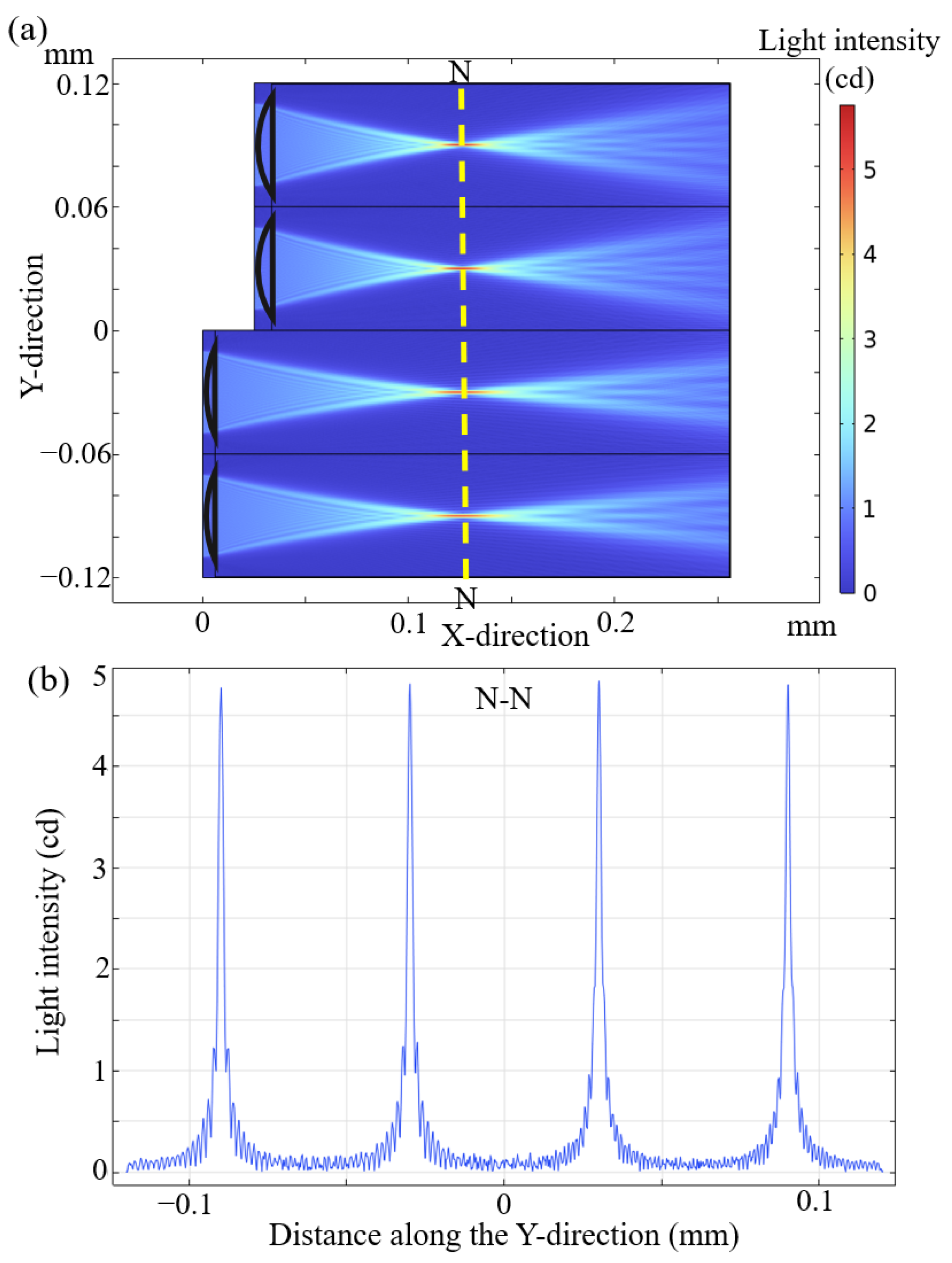
To fabricate stepped confocal microlens arrays, microlenses with distinct focal lengths and numerical apertures (NAs) must first be produced precisely. Accordingly, the influence of various laser processing parameters on microlens morphology was systematically investigated. Three critical parameters were identified to significantly affect the fabrication outcomes: laser focusing position, number of laser pulses, and pulse energy. To ensure the accuracy and repeatability of the experimental data, five parallel experiments were conducted for each set of processing parameters. The average values of microlens diameter and depth were then adopted as representative geometrical characteristics for calculating the corresponding focal length and NA.
The laser focusing position significantly influences the depth and spatial extent of the modified region, thereby affecting the resulting microlens diameter and depth. A single-factor experiment was conducted to examine the effect of focusing position on microlens morphology. The experimental parameters were fixed as follows: pulse energy of 15 μJ, 100 pulses, 20% hydrofluoric acid concentration, and a 4 h etching duration. The laser focusing positions were varied from −15 μm to +12 μm in increments of 0.5 μm. The laser focused on the glass surface was defined as Z = 0. A downward movement of the focal point along the z-axis was designated as Z < 0 (left side of Figure 5a), while an upward movement was designated as Z > 0 (right side of Figure 5a). The experimental results for microlens diameter (black squares) and depth (red dots) are presented in Figure 5a. As the focusing position increased, the microlens diameter initially increased, reaching a maximum between Z = −5 μm and 0 μm, and then decreased. In contrast, the microlens depth remained relatively stable initially and began to decrease near Z = 0. When Z < 0, significant fluctuations in depth were observed due to aberrations introduced by the intervening material prior to the laser reaching the focal plane. This aberration, caused by refractive index mismatch and laser energy absorption or attenuation, hinders stable energy delivery to the material, preventing it from reaching the ablation threshold and leading to greater depth variability under identical processing conditions. When Z < −5 μm (with a focal depth of ±5.15 μm), the laser spot transitioned from the surface into the bulk fused silica. This change in the dielectric interface altered the laser focusing characteristics, thereby modifying the nonlinear absorption of photon energy in the transparent medium and resulting in dimensional fluctuations of the microlenses. The average values from each parameter group were substituted into Equations (2), (3), and (4) to compute the microlens focal length and NA. As shown in Figure 5b, the focal length (black squares) increased with rising Z values, ranging from 70.06 μm to 121.67 μm, while the NA (red dots) decreased from 0.46 to 0.24. These results demonstrate that by adjusting the laser focusing position, both focal length and NA can be effectively tuned, with a focal length modulation range of 51.61 μm.
Additionally, both the number of laser pulses and the pulse energy influence the size of the modified region, thereby affecting the microlens diameter and depth. A single-factor experiment was performed to evaluate the effect of the number of pulses. Stable processing parameters were selected as follows: pulse energy of 15 μJ, a laser focus position of −10 μm, 20% hydrofluoric acid concentration, and a 4 h etching duration. The number of laser pulses ranged from 25 to 250 in steps of 25, and from 250 to 2500 in steps of 50. The resulting microlens diameters and depths are presented in Figure 5c. As the number of pulses increased, both the microlens diameter (black squares) and depth (red dots) showed a rising trend. Corresponding results for focal length and NA are shown in Figure 5d. With an increasing number of pulses, the focal length (black squares) exhibited a fluctuating downward trend, ranging from 146.02 μm to 91.56 μm, while the NA (red dots) increased from 0.17 to 0.37. These results indicate that by varying the number of pulses, the focal length and NA of the microlens can be effectively tuned, with a focal length modulation range of 54.46 μm. Moreover, the influence of pulse number on focal length variation is slightly more pronounced than that of laser focus position adjustment.
Finally, a single-factor experiment was conducted to investigate the effect of pulse energy, which varied from 11 μJ to 27 μJ in increments of 0.33 μJ, while all other parameters were maintained consistent with those used in the two previous experiments. The experimental results for microlens diameter (black squares) and depth (red dots) are presented in Figure 5e. As the pulse energy increased, both diameter and depth exhibited an upward trend. The corresponding focal length and NA results are shown in Figure 5f. With increasing pulse energy, the focal length (black squares) demonstrated a slightly increasing but fluctuating trend, whereas the change in NA (red dots) was relatively insignificant. The maximum variation range of focal length was 31 μm. The fluctuations in microlens morphology related to pulse energy are likely caused by multiple factors. During the interaction between the laser and the material, non-linear processes such as multi-photon absorption and avalanche ionization make the energy deposition in the material inconsistent. The mechanical stress generated by laser pulses can cause micro-structural changes in the material, and the thermal effects resulting from laser irradiation lead to non-uniform etching. All of these factors contribute to the instability of microlens morphology. Therefore, due to the pronounced fluctuations in the focal length curve, this method exhibits greater instability compared to the other two parameter adjustment methods. Therefore, pulse energy is not considered an optimal parameter for the precise regulation of microlens array focal lengths.
Etching time is another critical factor that influences the microlens geometry and optical performance. According to the growth behavior of the etched pit, the surface of the pit becomes smoother and gradually approaches a spherical shape only after a certain etching duration, thereby satisfying the geometric and optical requirements of microlens formation. To investigate this effect, we selected an initial etching time of 3 h and studied the variation in microlens diameter, depth, and focal length as the etching time increased. Based on preliminary experimental observations, the etching process requires a specific duration to stabilize during which the microlens surface smoothness meets optical requirements. However, excessive etching time adversely affects preparation efficiency. Therefore, the optimal etching duration was determined to be 3–8 h. The laser confocal images presented in Figure 6a illustrate the changes in microlens diameter under identical processing parameters at different etching durations. As etching time increases, the microlens diameter also increases. In the research, we focused on the relationships among etching time, pulse energy, and microlens diameter. After conducting a series of experiments with other parameters fixed, we analyzed the experimental data. The results show that within a certain range of etching time and pulse energy, the relationship between them and the microlens diameter can be described by an equation. When the etching time is between 3 h and 8 h and the pulse energy is between 6 μJ and 14 μJ, the equation is
D = 8 t + 5 E 34
where D represents the microlens diameter, t represents the etching time, and E represents the pulse energy. This equation is obtained through data fitting and can help us better understand and predict the changes in microlens diameter under different experimental conditions.
Figure 6b shows the corresponding variation in microlens depth, where different symbols (circles, pentagons, triangles, hexagons, and squares) represent pulse energies of 10 μJ, 11 μJ, 12 μJ, 13 μJ, and 14 μJ, respectively. The results indicate that microlens depth remains nearly constant over time, whereas the diameter continues to increase. This phenomenon occurs because the laser-modified region is entirely removed during etching, and the etching rates at both the pit bottom and surface are equal in the depth direction. As a result, the pit depth remains unchanged, while the diameter enlarges continuously due to the sustained lateral etching effect.
Based on the exploratory study of etching time, we first examined its influence on the microlens focal length. Figure 7a presents the variation in focal length under different etching durations. The pulse energy was set from 10 μJ to 20 μJ in increments of 1 μJ, while all other processing parameters were held constant to fabricate eleven microlenses. The results corresponding to various etching durations are color-coded as follows: red, orange, pink, green, blue, and purple denote etching times of 3, 4, 5, 6, 7, and 8 h, respectively. The focal length increases with etching time and exhibits an approximately linear relationship. The achievable focal length range spans from 61.82 μm to 178.49 μm, resulting in a maximum variation of 116.67 μm—exceeding the range adjustable by other individual processing parameters. Therefore, etching time provides an effective means for broader focal length modulation. In addition, since microlens diameter also varies significantly with etching time, we further plotted the focal length and diameter variations in microlenses at different pulse energies and etching durations to comprehensively illustrate the process capability. As shown in Figure 7b, where diameter is represented on the horizontal axis, focal length on the vertical axis, and color indicates etching time (consistent with Figure 7a), the outermost contour-enclosed region theoretically represent the achievable range through appropriate combinations of pulse energy and etching time. Figure 7a,b collectively demonstrate the relationship between etching time and microlens focal length and serve as a reference for customized microlens fabrication. For instance, to obtain microlens arrays with a high depth-to-diameter ratio and short focal length, the processing parameters indicated by the red stars (pulse energy of 10 μJ and etching time of 3 h) can be selected. Conversely, for microlens arrays with large apertures and long focal lengths, the parameters indicated by the purple stars (pulse energy of 20 μJ and etching time of 8 h) are preferable. In summary, the experimental results concerning laser processing parameters and etching time facilitate the delineation of the theoretical fabrication range for microlens arrays. This enables the selection of tailored processing conditions based on application-specific requirements, thereby allowing for the production of microlenses with desired dimensions and focal lengths through a well-defined mapping between process parameters and structural outcomes.

3.2. Simulation

To further investigate the focused beam characteristics of the SCMLA and validate the theoretical basis and effectiveness of its confocal imaging capability, simulation calculations were conducted using the designed structural parameters. The energy distribution of the focused beam produced by the SCMLA was simulated and analyzed using COMSOL Multiphysics 6.1 (COMSOL Inc., Burlington, MA, USA), a commercial finite element analysis software. As illustrated in Figure 8, a parallel beam with a wavelength of 500 nm is incident from the left and, after transmission through the microlenses, is focused within the air domain represented by the rectangular region on the right. The microlens parameters were derived from experimentally measured diameters and depths, and the refractive index was set to 1.41, corresponding to the refractive index of PDMS at a 500 nm wavelength. The upper and lower microlenses in the simulation correspond to the HMLA and LMLA configurations of the fabricated SCMLA, respectively. The simulated microlenses had diameters of 83 μm and 71 μm, with corresponding depths of 27 μm and 12 μm, respectively. A lateral shift of 25 μm was applied to the upper two microlenses relative to the lower two, corresponding to a step height of 25 μm. The simulation result shown in Figure 8a reveals that both the upper and lower microlenses focus the incident parallel beam at the same lateral position along the X-axis, confirming the confocal focusing effect of the SCMLA. Figure 8b presents the normalized energy distribution at the theoretical focal plane, as indicated by the yellow dashed line in Figure 8a and exhibits four distinct focal peaks of similar intensity corresponding to the focal points of the four microlenses, further substantiating the confocal imaging performance of the SCMLA.

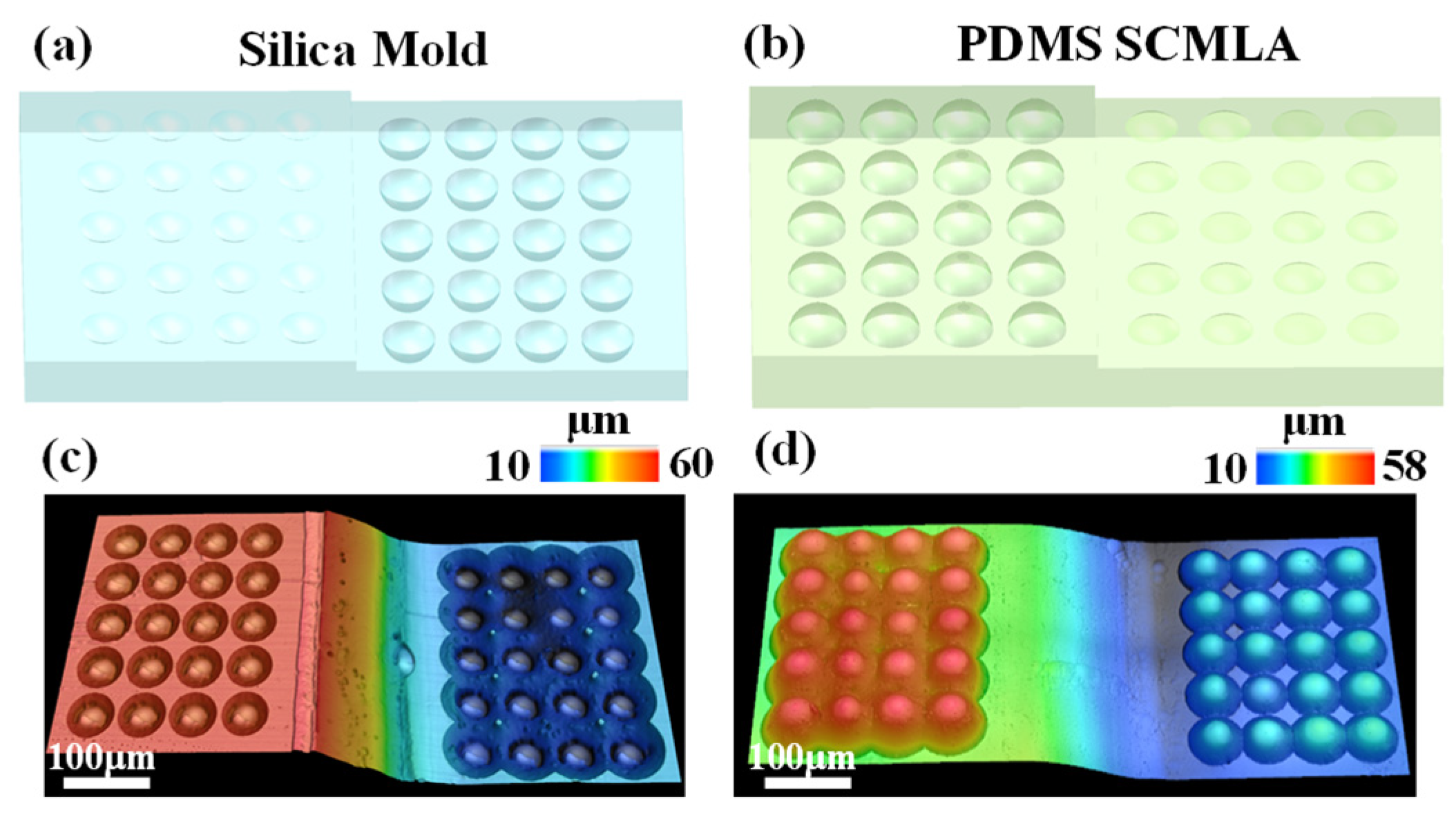
3.3. Fabrication and Imaging Characterization of SCMLA

Based on the established relationship between microlens processing parameters and focal lengths from previous experiments, an SCMLA with a step height of 25 μm was fabricated. The 25 μm step height was measured by stylus profilometer. The fused silica sample used measures 20 mm (length) × 20 mm (width) × 3 mm (thickness). A CO2 laser system (Changchun New Industries Optoelectronics Tech. Co., Ltd., Changchun, China) was employed for step processing, with a laser power of 30 W and a scanning speed of 100 mm/s. The higher microlens array (HMLA) exhibits a focal length of 100.01 μm and a numerical aperture (NA) of 0.42, while the lower microlens array (LMLA) has a focal length of 125.84 μm and an NA of 0.29. The confocal imaging capability of the two microlens arrays is realized by precisely controlling the focal length difference to approximately 25 μm. Figure 9a,b display the designed fused silica mold and the corresponding SCMLA replicated in PDMS through the molding process. Figure 9c presents the 3D laser confocal image of the fabricated mold, and Figure 9d shows the confocal topography of the SCMLA, in which the left HMLA and right LMLA exhibit distinct differences in microlens diameter and depth, consistent with the designed focal length and NA specifications.
The different focal lengths of the HMLA and LMLA were achieved by controlling distinct laser processing parameters while maintaining a constant etching time. Specifically, their focal positions were set to 0 μm and 10 μm, respectively, using a laser pulse energy of 15 μJ and 100 pulses. The etching concentration is 20% and the etching time is 4 h for both. Figure 10a illustrates the optical setup employed to evaluate the imaging performance of the SCMLA. A white light source is directed vertically upward from below, and the SCMLA focuses the transmitted light after it passes through an “F”-shaped mask. By adjusting the position of the upper objective lens along the beam propagation direction (denoted as the Z-direction in the figure) to coincide with the focal plane, the resulting focused image is projected onto the CCD camera coupled to the objective lens. The optical path of the imaging system is depicted in Figure 10f. Whether a clear image is formed depends on whether the focal plane aligns precisely with the sensor plane at the same position.
To provide a comparison with the SCMLA, two microlens arrays with different focal lengths were also fabricated on a flat surface. Figure 10b,d present the laser optical microscope observations and corresponding imaging results. As shown in Figure 10d, when the right microlens array is brought into focus through the objective lens, the left microlens array remains out of focus, indicating that simultaneous confocal imaging cannot be realized using this configuration.
The SCMLA was observed under an optical microscope, as shown in Figure 10c. When the HMLA was brought into clear focus, the LMLA appeared blurred due to the step height difference between the two arrays. The imaging performance of the SCMLA is presented in Figure 10e, where both the HMLA and LMLA produced sharp images simultaneously, successfully achieving the intended confocal imaging effect. From the magnified region of the “F” in Figure 10e, it is evident that the HMLA and LMLA exhibit different magnifications, with imaging widths of 19.3 μm and 20.5 μm, respectively, along with noticeable differences in brightness and resolution. These disparities arise from the distinct focal lengths and numerical apertures (NAs) of the two arrays. A longer focal length results in a smaller field of view (FOV) and shallower depth of field, while a higher NA enhances resolution and light collection efficiency. Consequently, the SCMLA provides multiple depths of field and multiple FOVs, enabling simultaneous multi-magnification and multi-resolution imaging. This capability allows for a more comprehensive acquisition of both light intensity and phase information within the captured image.

4. Conclusions

In summary, we propose a SCMLA fabricated using a femtosecond laser in combination with chemical etching and the PDMS molding method. The SCMLA offers the advantages of both single-focused microlens array confocal imaging and multi-focused microlens array multiscale imaging and optical aberration correction. The influence of focusing position, number of pulses, pulse energy, etching time, and other parameters on the optical performance of the microlenses is investigated through comparative experiments. The resulting microlenses can adjust the focal length in the range of 61.82 μm to 178.49 μm. The imaging effects of confocal plane imaging, multiple depths of field, multi-scale FOV, and multi-resolution are achieved, and the experimental results are in good agreement with the finite element simulation analysis. In the future, SCMLA will have significant potential for application and broad prospects in machine vision, spatial position imaging, and optical sensing, providing strong technical support for the rapid development of visual recognition optical systems.

Author Contributions

Conceptualization, J.W. and H.Z.; methodology, J.W.; software, Z.L.; validation, Z.L.; formal analysis, J.W.; investigation, J.W.; resources, H.Z.; data curation, H.W.; writing—original draft preparation, J.W.; writing—review and editing, H.W.; visualization, H.W.; supervision, H.Z.; project administration, J.W.; funding acquisition, H.Z. All authors have read and agreed to the published version of the manuscript.

Funding

Science and Technology Commission of Shanghai Municipality (23PJ1406600), National Natural Science Foundation of China Joint Fund Key Project (23Z031602524).

Institutional Review Board Statement

Not applicable.

Informed Consent Statement

Not applicable.

Data Availability Statement

Data underlying the results presented in this paper are not publicly available but may be obtained from the authors upon reasonable request.

Conflicts of Interest

The authors declare no conflicts of interest.

References

  1. Suleski, T.; Kolste, R. Fabrication trends for free-space microoptics. J. Light. Technol. 2005, 23, 633–646. [Google Scholar] [CrossRef]
  2. Hsu, C.J.; Antony, M.; Huang, C.Y. Laser beam homogenization based on a multifocal liquid crystal microlens array. Opt. Lett. 2024, 49, 670–673. [Google Scholar] [CrossRef]
  3. Cao, J.-J.; Hou, Z.-S.; Tian, Z.-N.; Hua, J.-G.; Zhang, Y.-L.; Chen, Q.-D. Bioinspired Zoom Compound Eyes Enable Variable-Focus Imaging. ACS Appl. Mater. Interfaces 2020, 12, 10107–10117. [Google Scholar] [CrossRef]
  4. Liu, X.; Yang, S.; Yu, L.; Chen, Q.; Zhang, Y.; Sun, H. Rapid Engraving of Artificial Compound Eyes from Curved Sapphire Substrate. Adv. Funct. Mater. 2019, 29, 1900037. [Google Scholar] [CrossRef]
  5. Wu, D.; Wang, J.N.; Niu, L.G.; Zhang, X.L.; Wu, S.Z.; Chen, Q.D.; Lee, L.P.; Sun, H.B. Bioinspired Fabrication of High-Quality 3D Artificial Compound Eyes by Voxel—Modulation Femtosecond Laser Writing for Distortion-Free Wide-Field-of-View Imaging. Adv. Opt. Mater. 2014, 2, 751–758. [Google Scholar] [CrossRef]
  6. Yuan, C.; Kowsari, K.; Panjwani, S.; Chen, Z.; Wang, D.; Zhang, B.; Ng, C.J.-X.; Alvarado, P.V.Y.; Ge, Q. Ultrafast Three-Dimensional Printing of Optically Smooth Microlens Arrays by Oscillation-Assisted Digital Light Processing. ACS Appl. Mater. Interfaces 2019, 11, 40662–40668. [Google Scholar] [CrossRef]
  7. Ko, C.H.; Lin, C.H.; Tsai, B.C.; Shih, H.H.; Wu, C.T.; Chao, Y.L.; Chou, Y.K.; Chu, C.H.; Chiou, Y.T.; Chen, R. Development of microlens arrays for high-speed optical communi-cation. Proc. SPIE 2004, 5454, 121–128. [Google Scholar]
  8. Li, K.; Huang, X.; Chen, Q.; Xu, G.; Xie, Z.; Wan, Y.; Gong, F. Flexible fabrication of optical glass micro-lens array by using contactless hot embossing process. J. Manuf. Process. 2020, 57, 469–476. [Google Scholar] [CrossRef]
  9. Lim, J.; Gruner, P.; Konrad, M.; Baret, J.-C. Micro-optical lens array for fluorescence detection in droplet-based microfluidics. Lab A Chip 2013, 13, 1472–1475. [Google Scholar] [CrossRef]
  10. Nakamura, M.; Mano, I.; Taniguchi, J. Fabrication of micro-lens array with antireflection structure. Microelectron. Eng. 2019, 211, 29–36. [Google Scholar] [CrossRef]
  11. Ratcliff, J.; Supikov, A.; Alfaro, S.; Azuma, R. ThinVR: Heterogeneous microlens arrays for compact, 180 degree FOV VR near-eye displays. IEEE Trans. Vis. Comput. Graph. 2020, 26, 1981–1990. [Google Scholar] [CrossRef]
  12. Joo, K.-I.; Park, M.-K.; Park, H.; Lee, T.-H.; Kwon, K.-C.; Lim, Y.-T.; Erdenebat, M.-U.; Lee, H.; Lee, G.; Kim, N.; et al. Light-Field Camera for Fast Switching of Time-Sequential Two-Dimensional and Three-Dimensional Image Capturing at Video Rate. IEEE Trans. Ind. Electron. 2019, 67, 6975–6985. [Google Scholar] [CrossRef]
  13. Zhang, Y. Exploring the autoinhibition mechanism of the C-terminal guanine nucleotide exchange factor module of Trio through molecular dynamics simulations. Chem. Phys. Lett. 2019, 730, 100–104. [Google Scholar] [CrossRef]
  14. Wang, W.; Chen, G.; Weng, Y.; Weng, X.; Zhou, X.; Wu, C.; Guo, T.; Yan, Q.; Lin, Z.; Zhang, Y. Large-scale microlens arrays on flexible substrate with improved numerical aperture for curved integral imaging 3D display. Sci. Rep. 2020, 10, 11741. [Google Scholar] [CrossRef]
  15. Cha, Y.-G.; Na, J.-W.; Kim, H.-K.; Kwon, J.-M.; Huh, S.-H.; Jo, S.-U.; Kim, C.-H.; Kim, M.H.; Jeong, K.-H. Microlens array camera with variable apertures for single-shot high dynamic range (HDR) imaging. Opt. Express 2023, 31, 29589–29595. [Google Scholar] [CrossRef]
  16. Chang, S.; Rioux, M.; Grover, C. Range face recognition based on the phase Fourier transform. Opt. Commun. 2003, 222, 143–153. [Google Scholar] [CrossRef]
  17. Derrode, S.; Ghorbel, F. Robust and Efficient Fourier–Mellin Transform Approximations for Gray-Level Image Reconstruction and Complete Invariant Description. Comput. Vis. Image Underst. 2001, 83, 57–78. [Google Scholar] [CrossRef]
  18. Li, Y.; Mund, M.; Hoess, P.; Deschamps, J.; Matti, U.; Nijmeijer, B.; Sabinina, V.J.; Ellenberg, J.; Schoen, I.; Ries, J. Real-time 3D single-molecule localization using experimental point spread functions. Nat. Methods 2018, 15, 367–369. [Google Scholar] [CrossRef]
  19. Stallinga, S.; Rieger, B. Accuracy of the Gaussian Point Spread Function model in 2D localization microscopy. Opt. Express 2010, 18, 24461–24476. [Google Scholar] [CrossRef]
  20. Chao, G.L.L.X.A. Synthetic Aperture Imaging Lidar Tran-receiver Optical System Based on Microlens Array. Acta Photonica Sin. 2023, 52, 1111002. [Google Scholar]
  21. Huang, K.-Y.; Wang, C.-F.; Shih, D.-L.; Chang, K.-P.; Chang, Y.-P.; Liu, C.-N.; Cheng, W.-H. Scheme of flash LiDAR employing glass aspherical microlens array with large field of illumination for autonomous vehicles. Opt. Express 2024, 32, 35854–35870. [Google Scholar] [CrossRef]
  22. Arai, J.; Kawai, H.; Okano, F. Microlens arrays for integral imaging system. Appl. Opt. 2006, 45, 9066–9078. [Google Scholar] [CrossRef] [PubMed]
  23. Cai, W.; Cheng, M.; Kong, D.; Ma, Z.; Liu, Y.J. Switchable liquid crystal lenticular microlens arrays based on photopolymerization-induced phase separation for 2D/3D autostereoscopic displays. Opt. Express 2023, 32, 625–638. [Google Scholar] [CrossRef] [PubMed]
  24. Ko, D.; Gu, B.; Ma, Y.; Jo, S.; Hyun, D.C.; Kim, C.S.; Oh, H.-J.; Kim, J. Characterization of optical manipulation using microlens arrays depending on the materials and sizes in organic photovoltaics. RSC Adv. 2021, 11, 9766–9774. [Google Scholar] [CrossRef] [PubMed]
  25. Li, P.; Liu, X.; Cheng, Q.; Liang, Z. Long-term photovoltaic performance of thin-film solar cells with diffractive microlens arrays on glass substrates. Results Phys. 2021, 21, 103841. [Google Scholar] [CrossRef]
  26. Luo, Y.; Wang, L.; Ding, Y.; Wei, H.; Hao, X.; Wang, D.; Dai, Y.; Shi, J. Direct fabrication of microlens arrays with high numerical aperture by ink-jetting on nanotextured surface. Appl. Surf. Sci. 2013, 279, 36–40. [Google Scholar] [CrossRef]
  27. Zang, Z.; Tang, X.; Liu, X.; Lei, X.; Chen, W. Fabrication of high quality and low cost microlenses on a glass substrate by direct printing technique. Appl. Opt. 2014, 53, 7868–7871. [Google Scholar] [CrossRef]
  28. Zhang, Q.; Schambach, M.; Jin, Q.; Heizmann, M.; Lemmer, U. Compact multispectral light field camera based on an inkjet-printed microlens array and color filter array. Opt. Express 2024, 32, 23510–23523. [Google Scholar] [CrossRef]
  29. Zhou, X.; Peng, Y.; Peng, R.; Zeng, X.; Zhang, Y.-A.; Guo, T. Fabrication of Large-Scale Microlens Arrays Based on Screen Printing for Integral Imaging 3D Display. ACS Appl. Mater. Interfaces 2016, 8, 24248–24255. [Google Scholar] [CrossRef]
  30. Yabu, H.; Shimomura, M. Simple Fabrication of Micro Lens Arrays. Langmuir 2005, 21, 1709–1711. [Google Scholar] [CrossRef]
  31. Xiao, G.; Zhang, X.; Lou, F.; Lei, L.; Cheng, X. Wide-angle vertical coupling gratings enabled by nano-imprinted microlens array. In Proceedings of the 2024 Optical Fiber Communications Conference and Exhibition (OFC), San Diego, CA, USA, 24–28 March 2024; p. W2B.9. [Google Scholar]
  32. Wang, M.; Yu, W.; Wang, T.; Han, X.; Gu, E.; Li, X. A novel thermal reflow method for the fabrication of microlenses with an ultrahigh focal number. RSC Adv. 2015, 5, 35311–35316. [Google Scholar] [CrossRef]
  33. Huang, S.; Li, M.; Shen, L.; Qiu, J.; Zhou, Y. Flexible fabrication of biomimetic compound eye array via two-step thermal reflow of simply pre-modeled hierarchic microstructures. Opt. Commun. 2017, 393, 213–218. [Google Scholar] [CrossRef]
  34. Liu, Y.; Li, X.; Wang, Z.; Qin, B.; Zhou, S.; Huang, J.; Yao, Z. Morphology adjustable microlens array fabricated by single spatially modulated femtosecond pulse. Nanophotonics 2021, 11, 571–581. [Google Scholar] [CrossRef] [PubMed]
  35. Wu, C.Y.; Chiang, T.H.; Lai, N.D.; Do, D.B.; Hsu, C.C. Fabrication of microlens arrays based on the mass transport effect of SU-8 photoresist using a multiexposure two-beam interference technique. Appl. Opt. 2009, 48, 2473–2479. [Google Scholar] [CrossRef]
  36. He, Z.; Lee, Y.-H.; Chanda, D.; Wu, S.-T. Adaptive liquid crystal microlens array enabled by two-photon polymerization. Opt. Express 2018, 26, 21184–21193. [Google Scholar] [CrossRef]
  37. Wang, B.-X.; Zheng, J.-X.; Qi, J.-Y.; Guo, M.-R.; Gao, B.-R.; Liu, X.-Q. Integration of Multifocal Microlens Array on Silicon Microcantilever via Femtosecond-Laser-Assisted Etching Technology. Micromachines 2022, 13, 218. [Google Scholar] [CrossRef]
  38. Liu, Y.; Qiao, Z.; Qu, D.; Wu, Y.; Xue, J.; Li, D.; Wang, B. Experimental Investigation on Form Error for Slow Tool Servo Diamond Turning of Micro Lens Arrays on the Roller Mold. Materials 2018, 11, 1816. [Google Scholar] [CrossRef]
  39. Zhang, X.; Chen, Z.; Chen, J.; Wang, Z.; Zhu, L. Fabrication of a microlens array featuring a high aspect ratio with a swinging diamond tool. J. Manuf. Process. 2022, 75, 485–496. [Google Scholar] [CrossRef]
  40. Yang, T.; Li, M.; Yang, Q.; Lu, Y.; Cheng, Y.; Zhang, C.; Du, B.; Hou, X.; Chen, F. Femtosecond Laser Fabrication of Submillimeter Microlens Arrays with Tunable Numerical Apertures. Micromachines 2022, 13, 1297. [Google Scholar] [CrossRef]
  41. Li, M.; Yang, Q.; Bian, H.; Yang, T.; Hou, X.; Chen, F. Microlens arrays enable variable-focus imaging. Opt. Laser Technol. 2022, 153, 108260. [Google Scholar] [CrossRef]
  42. Deng, C.; Kim, H.; Ki, H. Fabrication of a compound infrared microlens array with ultrashort focal length using femtosecond laser-assisted wet etching and dual-beam pulsed laser deposition. Opt. Express 2019, 27, 28679–28691. [Google Scholar] [CrossRef] [PubMed]
  43. Pan, A.; Chen, T.; Li, C.; Hou, X. Parallel fabrication of silicon concave microlens array by femtosecond laser irradiation and mixed acid etching. Chin. Opt. Lett. 2016, 14, 052201. [Google Scholar] [CrossRef]
  44. Zhang, F.; Yang, Q.; Bian, H.; Li, M.; Hou, X.; Chen, F. Fabrication of Chalcogenide Glass Based Hexagonal Gapless Microlens Arrays via Combining Femtosecond Laser Assist Chemical Etching and Precision Glass Molding Processes. Materials 2020, 13, 3490. [Google Scholar] [CrossRef] [PubMed]
  45. Zhang, F.; Yang, Q.; Bian, H.; Wang, S.; Li, M.; Hou, X.; Chen, F. Fabrication of a Chalcogenide Glass Microlens Array for Infrared Laser Beam Homoge-nization. Materials 2021, 14, 5952. [Google Scholar] [CrossRef]
  46. Bian, H.; Wei, Y.; Yang, Q.; Chen, F.; Zhang, F.; Du, G.; Yong, J.; Hou, X. Direct fabrication of compound-eye microlens array on curved surfaces by a facile femtosecond laser enhanced wet etching process. Appl. Phys. Lett. 2016, 109, 221109. [Google Scholar] [CrossRef]
  47. Zhou, W.; Li, R.; Li, M.; Tao, P.; Wang, X.; Dai, S.; Song, B.; Zhang, W.; Lin, C.; Shen, X.; et al. Fabrication of microlens array on chalcogenide glass by wet etching-assisted femtosecond laser direct writing. Ceram. Int. 2022, 48, 18983–18988. [Google Scholar] [CrossRef]
  48. Tian, Z.-N.; Yao, W.-G.; Xu, J.-J.; Yu, Y.-H.; Chen, Q.-D.; Sun, H.-B. Focal varying microlens array. Opt. Lett. 2015, 40, 4222–4225. [Google Scholar] [CrossRef]
Figure 1. (a) Schematic of conventional microlens array. (b) Schematic of planar multifocal microlens array. (c) Schematic of the SCMLA. (d) Schematic of the SCMLA fabrication process.
Photonics 12 00494 g001
Figure 2. (a) Schematic of the femtosecond laser processing system. (b) Experimental setup.
Photonics 12 00494 g002
Figure 3. (ac) Laser confocal microscopy images of microlenses etched for 20, 40, and 60 min. (d) Cross-sectional comparison between the actual microlens morphology and the ideal spherical contour.
Photonics 12 00494 g003
Figure 4. (a) Schematic of the formation process of microlenses mold on the lower step. (b) Schematic of the formation process of microlenses mold on the higher step.
Photonics 12 00494 g004
Figure 5. (a) Relationship between the diameter and depth of the microlens and the focusing position. (b) Relationship between the focal length and NA of the microlens and the focusing position. (c) Relationship between the diameter and depth of the microlens and the number of pulses. (d) Relationship between the focal length and NA of the microlens and the number of pulses. (e) Relationship between the diameter and depth of the microlens and the pulse’s energy. (f) Relationship between the focal length and NA of the microlens and the pulse’s energy.
Photonics 12 00494 g005
Figure 6. (a) Laser confocal images of microlenses with different etching times. (b) Diameter and depth of microlenses versus etching time (circles, pentagrams, triangles, hexagons, and squares represent pulse energies of 10 μJ, 11 μJ, 12 μJ, 13 μJ, and 14 μJ, respectively).
Photonics 12 00494 g006
Figure 7. (a) Variation in the microlenses’ focal lengths with etching time. (b) Diagram of the range of the microlenses’ processing capabilities. (The red, orange, pink, green, blue, and purple stars in a and b represent etching times of 3 h, 4 h, 5 h, 6 h, 7 h, and 8 h, respectively).
Photonics 12 00494 g007
Figure 8. Simulation of beam focusing characteristics of stepped microlenses using the finite element method. (a) The energy distribution of the beam is after the SCMLA focuses on it. (b) Distribution of beam energy at the theoretical focal point along the Y-direction.
Photonics 12 00494 g008
Figure 9. (a) The designed silica mold. (b) The designed SCMLA. (c) 3D laser confocal topography of the fused silica mold. (d) 3D laser confocal topography of the SCMLA.
Photonics 12 00494 g009
Figure 10. (a) Microlens array imaging optical system schematic. (b) Optical microscope observation of the planar multi-focus-MLA. (c) Imaging effect of the planar multi-focus-MLA. (d) Optical microscope observation of the SCMLA. (e) Optical microscope observation of the SCMLA. (f) Schematic of the imaging principle of the microlens array.
Photonics 12 00494 g010
Disclaimer/Publisher’s Note: The statements, opinions and data contained in all publications are solely those of the individual author(s) and contributor(s) and not of MDPI and/or the editor(s). MDPI and/or the editor(s) disclaim responsibility for any injury to people or property resulting from any ideas, methods, instructions or products referred to in the content.

