1. Introduction
Colloidal quantum dots (QDs) are a type of zero-dimensional nanoscale semiconductor material, and their sizes typically range from a few nanometers to several tens of nanometers [
1]. The nanoscale size of QDs strongly restricts the movement of electrons in all three dimensions [
2]. The quantum confinement effect endows QDs with unique optoelectronic properties [
3,
4]. Different from traditional bulk semiconductor materials, the energy band structure of QDs can be adjusted by precisely controlling their size and shape, thus enabling precise control of the emission wavelength [
5]. This allows QDs to emit light with a narrow linewidth and high purity, covering a wide spectral range from ultraviolet to infrared [
6]. In addition, QDs also possess advantages such as a high fluorescence quantum yield [
7], good photostability [
8], and biocompatibility [
9], which make them ideal materials for fabricating high-performance optoelectronic devices [
10,
11,
12]. Specifically, QDs are usually encapsulated by a shell of material with a wider bandgap [
13,
14,
15]. When core/shell QDs are excited by high-energy photons, the shell of the QDs can rapidly absorb the photons and transport the excitons to the core. This enhances the radiative recombination efficiency of the excitons. These characteristics make QDs widely applicable to the field of lasers [
16,
17]. Because this structure suppresses the non-radiative Auger recombination [
18,
19], the core–shell system has resulted in some reports of lower lasing thresholds [
18,
20,
21].
Particularly, QDs have excellent solution processability, which has attracted great interest in on-chip integrated optoelectronic devices [
22,
23,
24]. The assembly of colloidal nanocrystals provides an effective approach for constructing, designing, and integrating functional devices [
25,
26,
27]. The solution patterning method for fabricating microstructures is widely applied in fields such as materials science and micro–nano manufacturing [
28,
29,
30]. Its principle is to control the solution to form patterns in micro or nano sizes, which form the designed microstructures after the solvent evaporates. The most crucial aspect of the preparation process is the control of the solution dewetting process. Compared with traditional micro-structure manufacturing processes, solution patterning methods such as soft lithography [
31,
32] and inkjet printing [
33,
34] have the advantage of low costs and excel in wafer-scale integration and high-precision control. However, the disordered and uncontrollable dewetting dynamics during the solvent evaporation process reduce the quality of the finally formed patterned structures [
35], thereby reducing the performance of the devices. Directionally controlling the solution flow and the liquid contraction during the solvent evaporation process is crucial to achieving the orderly self-assembly and integrated application of QDs. This has given rise to other novel self-assembly technologies, such as electrowetting and flow-guided assembly. The electrowetting technology stands out due to its high-precision manipulation of droplets, rapid response capability, and good integrability, and it has great application value in fields such as microfluidic chips [
36,
37]. However, it requires a complex electrode structure, and the limitation of the threshold voltage on its efficiency remains a challenge that needs to be addressed [
38]. The flow-guided assembly technology does not require complex external equipment, adopts a non-contact manipulation method, and has good controllability [
39,
40]. Nevertheless, it should not be overlooked that this technology is sensitive to the shape and size of particles, resulting in a relatively limited range of applicable particle types.
In this study, we developed an asymmetric wettability template for controlling the directional flow of the solution and the ordered self-assembly of QDs. Based on this template, using colloidal CdSe/ZnS QDs as the material, we prepared large-area and high-quality self-assembled micro-ring structures. Excited by a femtosecond pulse laser, coherent photonic lasing with a low threshold () and a narrow linewidth (0.3 nm) was achieved in the ring resonators at room temperature. The measurement and analysis of the angle-resolved PL (ARPL) spectra revealed an obvious transition of the photon lasing behavior. Moreover, a destructive interference pattern similar to Young’s double-slit interference was observed, which further confirmed that the fabricated QD microcavities have high-quality lasing performance. Our results demonstrate that the self-assembled microstructures of QDs have great application prospects in the field of on-chip integrated all-optical devices.
2. Materials and Methods
The oil-soluble CdSe/ZnS core–shell QDs used in this research work were commercial products purchased from the market (Suzhou Xingshuo Nanotechnology Co., Ltd., Suzhou, China). Based on the solution self-assembled patterning method, we utilized the self-developed asymmetric wettability template to fabricate the QD micro-ring arrays. The periodically arranged micropillars in the template, which have hydrophobic sidewalls and hydrophilic tops, allowed for the generation of capillary bridges and the directional flow of the QD solution, thus enabling the ordered self-assembly of the QDs. In this way, an array of QD micro-rings with strict arrangement, precise position, tunability, and uniform size was fabricated. The template preparation and processing procedures were as follows: A micropillar array (with a radius of 6 μm, a width of 1.5 μm, and a height of 15 μm) was fabricated on a silicon wafer with photolithography and reactive ion etching. The template was successively cleaned with deionized water, ethanol, and isopropyl alcohol, then treated with oxygen plasma to remove contaminants, particles, and other impurities on the surface of the silicon wafer. A planar substrate coated with a photoresist (SU8, Kayaku Advanced Materials, Inc., Westborough, MA, USA) was pressed onto the micropillar template. Then, the planar substrate was peeled off, and the template with the adhered photoresist was baked at 95 °C for 3 min, leaving a SU8 protective layer on the top of the micropillars.
The treated template was placed in a glass petri dish, and heptadecafluorodecyltrimethoxysilane (FAS, Beijing J&K Scientific Ltd., Beijing, China) molecules were added. The template was infiltrated with the FAS solution at low pressure at room temperature for 24 h and then heated at 90 °C for 2 h to form a uniform hydrophobic surface in the gaps between the micropillars and on the sidewall regions, while the top area was protected by the photoresist and not affected. After modification with the FAS solution, the SU8 protective layer on the top of the micropillars was removed to obtain a micro-ring template in which the wettability of the top of the micropillars was different from that of the gaps between the sidewalls.
The fabrication method of capillary liquid bridges is limited by microstructure size for two reasons. In terms of the stability and precise control of capillary liquid bridges, as the micro-ring size decreases, capillary liquid bridges become correspondingly smaller. Their stability is extremely vulnerable to interference from tiny external factors, and it is more difficult to maintain the balance of internal forces within a liquid bridge. Additionally, the dewetting process is sensitive to parameter changes at small scales, making it difficult to achieve precise regulation. The other limitations are the solution and material properties. Small-sized micro-rings have extremely high requirements for the uniformity of the solution, and the aggregation of solutes or uneven concentration is amplified. For the micro-rings in this paper, this method could stably and with high quality fabricate micro-rings with a uniform morphology.
Scanning electron microscope (SEM) images of the CdSe/ZnS QD micro-rings were measured with a field emission scanning electron microscope (Zeiss Sigma, Carl Zeiss AG, Oberkochen, Germany). The fluorescence microscopy images of QD ring resonators were measured with a microscope (M330F-3M830F, Shenzhen AOSVI Optical Instrument Co., Ltd., Shenzhen, China) equipped with an ultraviolet lamp. To investigate the lasing properties of the QD micro-rings, the ARPL spectra were measured with a home-built ARPL system with a Fourier imaging configuration at room temperature. The samples were excited by a femtosecond pulsed laser (wavelength: 400 nm; repetition frequency: 1 kHz; pulse width: 80 fs). The pumping laser was focused on a spot with a diameter of 12 µm through a microscope objective. The PL emission was collected and sent into a spectrometer, Horiba iR550 (Horiba, Ltd., Kyoto, Japan), equipped with a 600-line/mm grating, and it was detected with a charge coupled device (CCD) of the Symphony II.
3. Results and Discussion
3.1. Optical Characterizations and Fabrication of CdSe/ZnS QDs
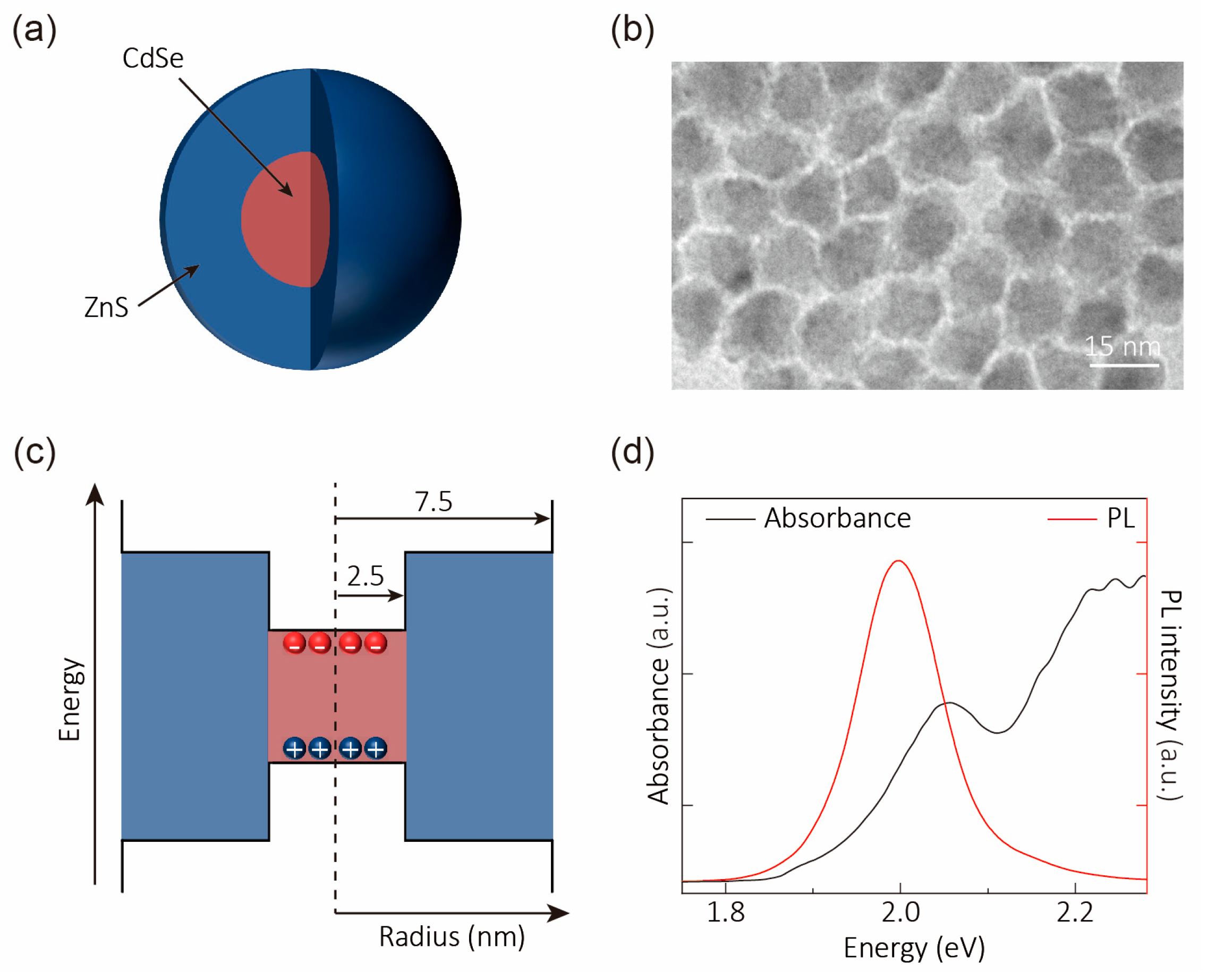
Optical gain materials are crucial and indispensable components for the construction of lasers. Colloidal QDs possess excellent optoelectronic properties and tunable characteristics, making them suitable for constructing the designed micro-ring structures to achieve the functions of lasers. The structure of the CdSe/ZnS (core/shell) QDs used in this paper is shown in
Figure 1a. The ZnS shell can effectively confine the excitons generated in the CdSe core within the core, thereby reducing the probability of non-radiative recombination and enhancing the luminescence efficiency [
41]. The size of CdSe/ZnS QDs was characterized with transmission electron microscopy (
Figure 1b). The average diameter of the QDs was 15 nm, which determined the energy band structure and emission wavelength of the QDs. The sizes of the QDs were uniform, which means that the quantum confinement effect was consistent. This could make the energy level distribution of electrons and holes relatively concentrated, making the emission wavelength more concentrated and narrowing the spectral width. The energy band structure of the CdSe/ZnS QDs is shown in
Figure 1c. CdSe/ZnS QDs are typical type I QDs. The CdSe core has a smaller bandgap than the ZnS shell, and the minimum of the conduction band and the maximum of the valence band of the core are lower and higher than those of the shell, respectively. The radius of the CdSe core is 2.5 nm, and the thickness of the ZnS shell is 2.5 nm. Electrons and holes generated in the CdSe core are effectively trapped within the core by the higher bandgap of the ZnS shell, enabling efficient radiative recombination and bright fluorescence emission. To further characterize the energy band structure and radiation process of the QDs, we measured the normalized PL and absorption spectra of the CdSe/ZnS QDs at room temperature (
Figure 1d). The PL spectrum exhibited an exciton emission peak centered at 2.0 eV (620 nm) with a linewidth of 37.3 nm, and the absorption spectrum showed a strong excitonic absorption centered at 2.05 eV (604.9 nm). Due to the existence of the Stokes shift, the energy of the absorption peak was higher than that of the PL peak. The QDs exhibited stable luminescence, high luminescence intensity, and high purity of the luminescent color.
3.2. Preparation and Characterization of the QD Micro-Rings
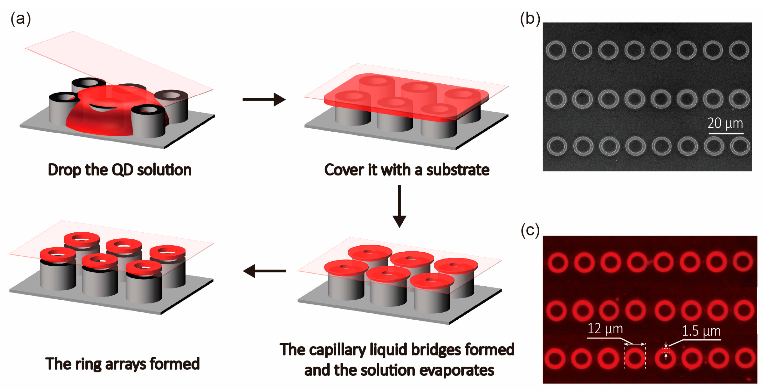
By adjusting the dewetting process of capillary liquid bridges, the self-assembly of QDs can be precisely controlled to form elaborate patterned structures. We applied this method to fabricate CdSe/ZnS (core/shell) QD micro-ring resonators. In this paper, an asymmetric wettability template was developed, and the directional flow and dewetting of the solution were successfully achieved through artificial control. The periodically arranged micropillars in the template, which have hydrophobic sidewalls and hydrophilic tops, allowed the generation of capillary bridges and the directional flow of the QD solution, thus enabling the ordered self-assembly of the QDs. The specific process is shown in
Figure 2a. First, drop 7 μL of the CdSe/ZnS QD solution onto the template and then cover it with a flat substrate to form a sandwich structure, ensuring that the QD solution fully covers the entire micro-ring template. Clips can hold the template and the substrate together to ensure sufficient contact between the solution and the template. Then, the sample is placed in an environment with constant temperature and pressure at room temperature for 6 h. Due to the internal capillary force, the liquid film sandwiched in the middle takes on a periodically concave meniscus shape. The ring array gradually forms as the liquid evaporates, and the gaps between the micro-rings continuously increase. Eventually, the film overflows to form individual liquid bridges fixed between the micro-ring tops and the substrate. Continuous dewetting within a single liquid domain leads to the contraction of the liquid with a high aspect ratio, ultimately resulting in the breakage of the liquid bridges. After the liquid completely evaporates and the QDs self-assemble, the entire micro-ring array appears on the substrate. Peeling off the template, a set of high-quality ring resonators is obtained.
We carried out morphological and luminescence characterizations of the prepared QD micro-rings. As shown in
Figure 2b, the scanning electron microscope image of the QD micro-rings exhibits excellent morphological quality. The micro-ring surface is smooth, and its uniformity is great. The ring diameter and width are 12 μm and 1.5 μm. The fluorescence microscope image shows that the QD micro-rings emitted light strongly and uniformly, which benefits from their excellent morphological quality and the stability of self-assembly (
Figure 2c). Thus, we successfully fabricated high-quality QD ring resonators using the solution self-assembly patterning method.
3.3. Lasing Characterizations of the QD Micro-Rings
After obtaining high-quality ring resonant cavities and great emission attributes, we demonstrated room-temperature lasing phenomena in the QD micro-rings excited by an ultrafast femtosecond pulse laser (400 nm, 1 kHz) at room temperature. The power-dependent PL mapping image and PL spectra of a QD micro-ring are shown in
Figure 3a. At a low pump fluence of
, the micro-rings emitted light resulting from the spontaneous emission (SE) of CdSe/ZnS QDs with a relatively wide linewidth. The PL peak is located at 620 nm, and the FWHM is 37 nm. With the pump fluence increasing to
(the threshold,
), one bright peak abruptly appears at the low-energy edge of the SE band (at 638.3 nm). This peak has a high intensity and an extremely narrow linewidth. With a further increase in pump fluence, the sharp peak becomes dominant in the PL spectra, with the intensity growing rapidly. At the same time, more high-energy lasing modes were amplified by the ring resonator and appeared at 632.7 nm, 627.7 nm, and 622.6 nm. The stable lasing mode needs to meet the standing-wave condition. The optical path of our micro-ring was
, where
R is the radius of the micro-ring and
is the effective refractive index. The standing-wave condition requires
(
is the mode number and
is the resonant wavelength), which can be deduced that
(
is the resonant frequency). The interval between two adjacent resonant frequencies can be obtained as
. The calculated mode frequency interval was
Hz, consistent with the lasing mode spacing, as shown in
Figure 3a. With the micro-ring size gradually decreasing, the interval between two adjacent frequencies continuously increased.
The nonlinear behaviors of the PL emission above and below the threshold indicate the lasing action in the QD micro-ring. To quantify the lasing behaviors of micro-rings, we analyzed the power-dependent PL intensity and linewidth of the lasing mode at 638.3 nm with the pump fluence range from
to
, respectively (
Figure 3b). In
Figure 3b, the integrated PL intensity as a function of the pump fluence shows a significant nonlinear enhancement with the change of the pump fluence. It increases by nearly two orders of magnitude above the lasing threshold (
) and exhibits a typical S-shaped trend. The PL linewidth significantly shrinks from 37.3 nm to 0.3 nm when the pump power passes through the lasing threshold. The typical two-stage shape power-dependent emission relationship demonstrates a distinct transition from SE to lasing emission. Moreover, the quality of our QD micro-rings can be quantified by the factor of Q = λ/Δλ, where λ is the wavelength of light and Δλ is the linewidth of the resonant modes. We extracted the linewidth of the lasing mode at 638.4 nm (corresponding to
Figure 3b) and calculated its Q to be 1928. This Q is larger than those QD resonators reported previously [
42].
The analysis of the lasing emission mechanism reveals that the micro-ring structure forms a high-quality whispering-gallery microcavity. When the excitation power increases to the lasing threshold, the gain within the microcavity is greater than the loss, resulting in laser oscillation. To further prove the generation of lasing, we measured the real-space images of the QD micro-ring above and below the threshold. Below the threshold (
), the micro-ring emitted light in all directions due to spontaneous emission, forming a donut shape (
Figure 3c). Above the threshold (
), population inversion was achieved in the micro-rings, realizing lasing that oscillated within the ring resonators. The real-space image of the QD micro-ring exhibits a uniform, bright, and petal-like light field distribution due to the standing wave distribution of WGMs in the ring resonator (
Figure 3d). These behaviors exhibit the typical characteristics of the lasing process and demonstrate the realization of room-temperature lasing in the QD micro-ring. Due to some inevitable losses and defects in the QD micro-ring, there was a leakage of the lasing signal at defect positions. Our results demonstrate the high-quality and excellent photonic lasing emission in our QD micro-rings at room temperature. Subsequently, the interference pattern of the lasing mode can be observed from the ARPL measurement (
Figure 4), which experimentally verifies the oscillation of the lasing in the micro-rings.
3.4. The Coherence of QD Micro-Ring Lasing
To analyze the coherence of the lasing in the QD micro-ring, we measured the ARPL spectra above and below the threshold. The effect measured in the experiment was analogous to Young’s double-slit interference, as shown in
Figure 4a. The lasing emission from the opposite sides of the QD micro-ring can be regarded as two coherent spotlight sources in real space. The light emitted from different positions on the micro-ring was collected by the objective and focused onto the slit of the spectrometer. Below the threshold, the ARPL spectrum shows that the PL of the micro-ring radiated over a wide range of angles with a wide bandwidth at
, corresponding to the PL spectrum mentioned above (
Figure 4b). The PL emitted by the micro-ring did not possess coherence. Above the threshold, population inversion was achieved in the micro-ring, leading to the generation of the lasing modes, which exhibited high coherence at
. The ARPL spectral pattern of the lasing oscillation modes is shown in
Figure 4c. The same lasing mode emitted by the upper and lower sides of the micro-ring interfered with each other in the back focal plane of the objective, resulting in the formation of bright and dark stripes in the Fourier space (
k-space). It is worth noting that the interference pattern of bright and dark stripes presented in the ARPL spectrum spread as the detection angle increased and only appeared in the lasing oscillation modes, corresponding to 638.3 nm, 632.7 nm, and 627.7 nm. The ARPL spectrum exhibits obvious interference patterns within a large angular range, and the contrast is relatively high. The PL intensity at 632.7 nm in the ARPL spectrum was extracted from the interference pattern, as shown in
Figure 4d. As a function of the detection angle, a destructive interference pattern with a periodic distribution and an intensity drop is presented at the detection angle of 0°. The optical paths from the opposite sides of the QD micro-ring to the 0° position of the interference plane are equal. The bright and dark fringes were determined by the phase difference of the light fields between the two spotlight sources. Therefore, the destructive interference at the 0° position of the ARPL spectrum indicates that the phase difference of the light fields on both sides of the QD micro-ring was an odd multiple of π.
The ARPL interference pattern presents an uneven and non-standard state, mainly due to the following two reasons: (1) The stray light collected by the microscopic objective lens covered part of the lasing modes. Due to the small size of the QD micro-rings and the relatively close arrangement between the micro-rings, the emitted light scattered from the inner and outer sidewalls of the micro-rings, as well as a small portion of the emitted light from other micro-rings, caused the characteristic signals of the resonant laser modes collected on the Fourier plane not to come solely from the front side of a single micro-ring. In this way, the ideal two-beam interference pattern was affected by other adjacent optical signals, showing broadening or displacement. (2) Deviations and fluctuations in the optical measurement system may also have been part of the reasons for the non-uniformity, which are related to the collimation of the collection optical path and the relative position between the sample and the slit of the spectrometer. Nevertheless, the characteristics of the interference pattern remain remarkably distinct. These experimental results indicate that lasing with high coherence was achieved in the prepared QD micro-rings.
Our QD micro-rings, with their excellent optical properties and a remarkably high Q of 1928, demonstrate application potential in optical communication and integrated optical chips. In optical communication, the lasing characteristics of QD micro-rings, such as the narrow linewidth (0.3 nm) and high coherence, make them promising as ideal light sources for high-speed and high-coherence optical transmission. In the field of integrated optical chips, the self-assembly of the QD micro-rings achieved through the solution patterning method is highly compatible with on-chip integration technology, which is conducive to reducing the size of optoelectronic devices and their power consumption and to promoting the development of optical computing and optical sensing chips towards miniaturization and high performance.
4. Conclusions
In conclusion, we successfully fabricated high-quality CdSe/ZnS QD self-assembled micro-ring resonators by using the solution patterning method with an asymmetric wettability template. Using the developed asymmetric wettability template, the directional flow of the liquid and controllable dewetting were successfully achieved, thus precisely controlling the geometric shape and position of the self-assembly of QDs. The fluorescence microscopy and SEM images demonstrate the excellent morphological quality and luminescent properties of the QD micro-rings. We directly observed coherent photon lasing with a low threshold () and a narrow linewidth (0.3 nm) in the QD micro-rings due to population inversion. Through Young’s double-slit interference method based on the far-field Fourier optical system, the interference pattern of the ARPL spectra of the coherent lasing showed destructive interference, revealing the optical field distribution of the lasing mode in the micro-ring cavity. Our experiments demonstrate the feasibility of applying the solution patterning method to the controllable self-assembly of QDs, providing a practical approach for fabricating the integrated self-assembled QD optoelectronic devices. This is expected to boost the development of optoelectronic devices with micro–nano structures.

