Abstract
Despite significant progress, fabricating two-dimensional (2D) lithium niobate (LN)-based photonic crystal (PhC) cavities integrated with tapered and PhC waveguides remains challenging, due to structural imperfections. Notable, especially, are variations in hole radius (r) and inclination angle (°), which induce bandgap shifts and degrade quality factors (Q-factor). These fabrication errors underscore the critical need to address nanoscale tolerances. Here, we systematically investigate the impacts of key geometric parameters on optical performance and optimize a 2D LN-based cavity integrated with taper and PhC waveguide system. Using a 3D Finite-Difference Time-Domain (FDTD) and varFDTD simulations, we identify stringent fabrication thresholds. The a must exceed 0.72 µm to sustain Q > ; reducing a to 0.69 µm collapses Q-factors below , due to under-coupled modes and bandgap misalignment, which necessitates ±0.005 µm precision. When an r < 0.22 µm weakens confinement, Q plummets to 2 × at r = 0.20 µm (±0.01 µm etching tolerance). Inclination angles < 70° induce 100× Q-factor losses, requiring ±2° alignment for symmetric modes. Air slot width (s) variations shift resonant wavelengths and require optimization in coordination with the inclination angle. By optimizing s and the inclination angle (at 70°), we achieve a record Q-factor of 6.21 ×, with, in addition, C-band compatibility (1502–1581 nm). This work establishes rigorous design–fabrication guidelines, demonstrating the potential for LN-based photonic devices with high nano-fabrication robustness.
1. Introduction
PhC optical cavities are highly regarded for their remarkable capacity to confine light and facilitate interactions with matter at scales smaller than the wavelength of light, paving the way for significant advancements in fields such as signal processing, bio-sensing, and quantum electrodynamics [1,2,3,4,5]. Among the various PhC structures, 2D PhC optical cavities are especially noteworthy. They excel in enhancing the density of photonic states, creating the potential for versatile device designs, and supporting scalable optoelectronic integration. Their compatibility with contemporary nanofabrication technologies has driven extensive research and cultivated strong interest across different material platforms [1,2,3,4,5,6,7,8,9,10,11]. LN, often called the “silicon of photonics”, exhibits remarkable properties, including electro-optic, nonlinear optical, acousto-optic, piezoelectric, photorefractive, pyroelectric, and photoconductive behaviors [12,13]. Its versatility has made LN widely applicable across various fields, such as telecommunications [14], nonlinear quantum photonics [15,16], micro-electromechanics [17,18], information storage [19,20], and sensing technologies. This flexibility makes it an ideal candidate for numerous applications [21,22]. Silicon-on-insulator (SOI) PhC cavities dominate the field due to their ultra-high quality factors (>10⁷) and mature fabrication processes [23,24], enabling low-loss, mass-producible photonic circuits. However, LN enables electro-optic tunability, strong nonlinearity for frequency conversion, and broad transparency (visible to mid-infrared), offering functionalities unattainable in passive SOI devices.
In recent years, LN-based PhC cavities with taper and PhC waveguides have emerged in nano photonics as promising platforms for the enhancement of light–matter interactions and the achievement of high-performance photonic devices. A substantial number of studies have systematically investigated and advanced the design [25,26,27,28,29,30,31], fabrication [32,33,34,35,36,37,38,39], and integration [40,41,42,43,44,45,46,47,48,49] of this device. However, due to strong physical and chemical inertness and the nature of the potential contamination, the fabrication process faces significant challenges, some of which lead to large structural imperfections. One key hurdle lies in integrating inclined LN cavities with PhC waveguides, for which alignment tolerances demand sub-10 nm positional precision during EBL. Such precision is limited by inherent EBL drift and proximity effects, which exacerbate coupling losses between the cavity and waveguide modes. Furthermore, deviations in the target inclination angle (e.g., 70°) beyond ±0.5° disrupt phase-matching conditions, significantly degrading nonlinear optical efficiency. Sacrificial layer etching introduces additional mechanical instability due to stress concentration at inclined interfaces, risking structural deformation or fracture. These issues greatly affect the performance of the devices, including matters relating to the optical quality factors and resonant wavelength. To address these tolerances, we present a parametric investigation of a 2D LN-based optical cavity integrated with a tapered waveguide and PhC waveguides featuring a 70° inclination angle. By simulating bandgap characteristics and transmission efficiency, we analyze the inclination angle’s impact on optical mode confinement and the Q-factors. This study offers a detailed performance analysis of this integrated PhC optical cavity design.
2. Fabrication and Structural Imperfections of 2D LN PhC Cavities
The fabrication process utilized EBL for nanoscale patterning and ICP etching to achieve precise geometric control, ensuring minimal sidewall roughness and the structural fidelity critical to high-Q performance. The fabrication process begins with the cleaning of the LN substrate to remove surface contaminants, ensuring an optimal foundation for subsequent layers. A photoresist layer is uniformly applied via spin coating and precisely patterned using EBL. After development, the exposed photoresist regions are removed, forming a high-resolution mask for etching. ICP etching transfers the intricate patterns into the LN device layer, after which the residual photoresist is stripped, revealing the structured LN layer. The sacrificial layer is then selectively etched to release the fabricated LN device, finalizing its mechanical and functional independence. This methodology employs advanced techniques such as EBL and selective etching, ensuring high precision and reproducibility. Figure 1a illustrates the schematic of the layered structure, which comprises a 0.3 μm LN device layer, a 0.2 μm silicon dioxide (SiO2) intermediate layer, and the LN substrate. Figure 1b–d present scanning electron microscopy (SEM) images of the fabricated device, confirming the achievement of precise control over the structural parameters. Notably, the inclination angle of 71.6° critical for achieving phase-matching conditions in optical applications is consistently realized.
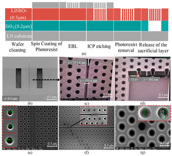
Figure 1.
The fabrication process of an LN-based device on an LN substrate. (a) Schematic representation of the layered structure, consisting of a 0.3 μm LN layer, a 0.2 μm silicon dioxide (SiO2) layer, and a LN substrate. (b) SEM image of the 2D LN-based integrated PhC optical cavity with an inclination angle of 71.6°. (c) Close-up view of the air slot, highlighting its dimensions, with a height of 375.6 nm and a width of 314.7 nm. (d) Detailed illustration of the inclination angle of 71.6°, demonstrating its critical role in optimizing the optical performance of the cavity. (e) SEM image revealing fabrication-induced irregularities in air-hole dimensions, a factor which may degrade optical resonance quality. (f) Close-up of non-uniform etching, showing variations in air-hole depth and morphology that could lead to inconsistent light–matter interactions. (g) Cross-sectional SEM image highlighting structural defects, including rough sidewalls and residual sacrificial material, potentially compromising mechanical stability and optical efficiency. This figure underscores the necessity for precision in design, etching, and process control to realize high-performance LN photonic devices.
Additionally, Figure 1 identifies critical fabrication errors that degrade the structural integrity and optical performance of LN PhC cavities. In Figure 1e, nonuniform feature dimensions and irregular edge profiles arise from inconsistent spin-coating (e.g., resist thickness variations > 15%) during electron-beam resist deposition (EBL) due to dose miscalibration, leading to localized over-underexposure. Radius deviations of 11.7 nm occur across multiple lattice points. Figure 1f highlights the nanoscale voids and incomplete etching patterns caused by nonoptimal ICP parameters, such as imbalanced /Ar gas ratios (>4:1) or insufficient RF power (<300 W). Figure 1g reveals residual circular defects, including persistent resist residue and incomplete sacrificial layer removal, originating from incomplete lift-off processes and due to insufficient resist development time (<90 s) or inadequate plasma etching. These imperfections induce radius shifts of 19.5 nm. These step-specific imperfections underscore the need for targeted refinements—including spin-coating speed optimization, EBL dose calibration, and ICP parameter tuning—to achieve sub-10 nm geometric fidelity in high-performance LN devices.
Simulation-Driven Tolerance Analysis of Critical Fabrication Errors
This study analyzed three critical fabrication errors in 2D LN-based PhC optical cavities, prioritizing their impact on performance by using 3D FDTD (version 2024): (1) positional offsets of air holes in the microcavity area, modeled via 1–3 nm global offsets or 3 nm offsets in subsets of holes, which disrupt mode field symmetry and induce large resonant wavelength deviations near the cavity center due to strong field localization (Figure 2a); (2) dimensional deviations in air-hole radii across the entire structure, simulated by replacing circular holes with polygonal apertures (8–24 sides, roundness 7.61–0.9%), perturbing the global photonic bandgap (Figure 2b); and (3) Thickness nonuniformity in specific regions, introduced as +20 nm, +40 nm, or +60 nm variations, which degrade mode confinement, as shown in Figure 2c. The key findings reveal that positional offsets near the microcavity center cause the largest wavelength shifts, while dimensional deviations and thickness errors result in partial tolerance in narrow-bandgap regions. The work underscores the necessity for stringent geometric control, particularly near the cavity core, to mitigate nonlinear frequency responses driven by PBG dielectric gradients.
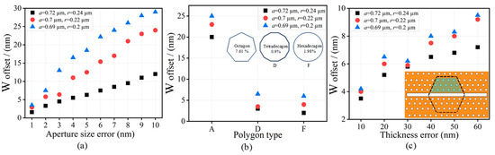
Figure 2.
(a) Correlations between resonant wavelength shifts and air-hole radius deviations. (b) Regular polygonal apertures (showing their roundness) and correlations between resonant wavelength shifts and roundness distortions. (c) Thickness variation types within the PhC optical cavity and correlations between resonant wavelength shifts and thickness variations.
This section, introducing various defects in PhC structures, is significant for several reasons. Firstly, exploring defects is crucial for practical applications, as real-world conditions often lead to imperfections that can significantly affect performance. Understanding how these defects interact with the intended design helps in assessing the robustness and reliability of photonic devices under realistic operational conditions. Additionally, defects can give rise to unique optical phenomena, such as localized modes or bandgap modifications, which may enhance or degrade PhC performance; investigating these effects allows researchers to develop strategies to mitigate negative impacts while leveraging potential benefits. Ultimately, integrating defect analysis provides a comprehensive understanding of the PhC structures, thus making the study more relevant and applicable to actual device implementations, contributing to the development of more effective photonic devices.
3. Investigation of LN-Based Taper Waveguide Integrated with PhC Waveguides
3.1. Bandgap Investigation for the 2D PhC Slab
The PhC slab designed in this study is based on an LN platform. The inset in Figure 3a illustrates the PhC slab prototype with defined structural parameters, where a represents the lattice constant, r denotes the radius of the air holes, and z indicates the thickness. Additionally, the inclination angle of the structure is denoted as (°). Figure 3a also presents the normalized bandgap width, /, where is the bandgap width and is the center frequency of the bandgap. The normalized bandgap width is calculated relative to . Our investigation focused on the influence of the inclination angle on key structural parameters, including a, r, and z. We observed that the inclination angle significantly affects the bandgap width. As the r decreases, the bandgap width increases, in correlation with the inclination angle, as shown in Figure 3a. Specifically, the bandgap width decreases with decreasing inclination angle. As the a increased, the bandgap width decreased in correlation with the inclination angle, as shown in Figure 3b. Furthermore, notable variations in the bandgap width were observed for different inclination angles and z, as illustrated in Figure 3c. These results demonstrate that as the inclination angle decreases from 90° to 45°, the maximum bandgap width exhibits a significant reduction. This trend is clearly illustrated in Figure 3a–c, in which the curves show an overall downward shift with decreasing inclination angles. Specifically, when the inclination angle reaches 45°, the bandgap width is reduced by approximately 50%, compared to the case of an inclination angle of 90°. Based on the simulation results, we optimized the structural parameters and achieved a narrow bandgap for LN-based PhC structures operating in the 1502–1581 nm wavelength range, as shown in Figure 3d. The optimized parameters are as follows: a at 0.72 μm, r at 0.24 μm, and z at 0.3 μm. The selected parameter ranges are as follows: fixed a at 0.72 µm, with a from 0.69 µm to 0.72 µm, and fixed r at 0.24 µm, and r from 0.2 µm to 0.24 µm; these were informed by preliminary eigenmode and 3D FDTD simulations, and attempted to balance high Q-factors >106 with fabrication feasibility (Table 1). Additionally, these ranges align with the LN-specific fabrication constraints identified in the literature [26,27,28,29]. These references provide empirical validation for the parameter bounds, ensuring that our design aligns with scalable LN nanofabrication practices. This study provides valuable insights into the relationships between structural parameters, inclination angles, and bandgap characteristics in LN-based PhC structures. These findings contribute to the design and fabrication of advanced photonic devices for optical communication and sensing applications.
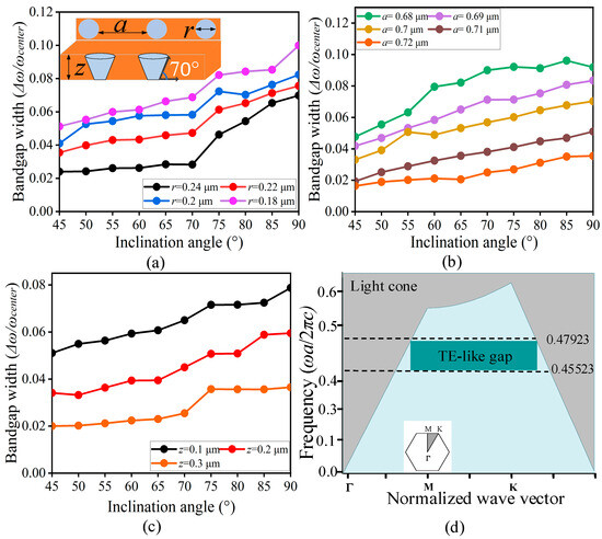
Figure 3.
Influence of structural parameters on the bandgap width of the LN-based PhC slab: (a) normalized bandgap width as a function of the hole radius; the inset shows the 2D PhC prototype with structural parameter definitions; (b,c) normalized bandgap width as a function of lattice constant and slab thickness; (d) a successful narrow-bandgap PhC structure operating in the 1502–1581 nm band.

Table 1.
Summaries of the key simulation parameters.
The optimized bandgap parameters and operational wavelength range of 1502–1581 nm establish a foundation for integrating LN-based PhC structures into functional photonic devices. However, practical implementation requires efficient coupling between conventional waveguides and the high-Q PhC cavity to minimize insertion losses while preserving bandgap-engineered performance. Achieving this demands an adequate design of the adiabatic taper, which bridges the mode mismatch between input waveguides and the PhC lattice. In Section 3.2, we analyze how taper geometry—specifically widths and —interacts with the inclination angle and the PhC bandgap to maximize transmission efficiency. This ensures that the cavity’s theoretically sufficient performance, rooted in its optimized bandgap, translates into robust experimental functionality.
3.2. Impacts of Taper Geometry and Inclination Angle on Waveguide Transmission Efficiency
Photonic bandgap (PBG) waveguides are advanced structures created by introducing a defect into a PhC, creating a periodic refractive index variation. This creates a bandgap that prevents light from propagating [50]. By altering the periodicity, specific wavelengths can be guided along the path created by the defect. This process utilizes the Bragg effect, in which waves are reflected within periodic structures, creating bandgaps through constructive interference [51,52]. This controlled light propagation is essential for optical communication and photonic circuits, and enables the development of efficient, compact, and high-speed optical devices [53,54]. In [27], the author shows the relationships between the structural parameters of lattice constant, radius, and slab thickness in LN-based PhC, and their bandgap structure. The author analyzed the specific effects of these three parameters on the bandgap structure. Based on the results of the analysis, a wide-bandgap LN-based 2D PhC was designed to operate in the 900 nm band.
The efficient optical coupling between two waveguides within the on-chip optical path can be achieved by a tapered waveguide, and the coupling efficiency can be controlled by the length and shape of the tapered waveguide. The geometric design of LN-based taper and PhC waveguides, particularly the inclination angle, is of utmost importance in determining their functionality and performance. The first step in designing an LN-based taper and PhC waveguide is to ensure that its operating wavelength range contains the required wavelengths. This is accomplished by simulating the bandgap of the PhC waveguide, which is the range of wavelengths that cannot propagate through the periodic structure. Simulations were performed using varFDTD engines, (version 2024) employing a hybrid 2.5D approach to efficiently model 3D electromagnetic effects. This hybrid 2.5D approach balances computational efficiency and accuracy by resolving vertical mode confinement through eigenmode analysis while modeling in-plane interactions with adaptive meshing. The simulation domain spanned 40 µm in the x-direction, 10 µm in the y-direction, and 3 µm in the z-direction, with Perfectly Matched Layer (PML) boundaries applied 1 µm from all domain edges to suppress numerical reflections. A high-accuracy adaptive mesh (accuracy level 5) was implemented to ensure a minimum grid step of 2 nm at critical interfaces (waveguide cores and air holes) and a maximum step of 20 nm in homogeneous regions. The material properties of LN were imported from Lumerical’s database, from which we also imported the LN index file to capture the refractive index modeled at λ = 1550 nm. Eigenmode calculations were deemed converged at a residual threshold of 1 × , ensuring numerical stability while effectively capturing dominant physical phenomena such as cavity resonance and taper coupling, which are critical to the study.
The tapered waveguide, shown in Figure 4a, has an input width , an output width connected to the PhC waveguide, a total length , and a parameter m that controls how smoothly the width transitions from to . This gradual width change minimizes optical loss and ensures efficient coupling to the cavity. The taper waveguide is defined below. This figure also shows the PhC waveguide, where w represents the distance between the centers of adjacent air holes. Normally, w = k* √3 a; here, we set k at 1.2, so it can be determined that the value of w can be 1.2 μm, a value which is constant throughout the simulation. Accordingly, we set a at 0.72 μm.
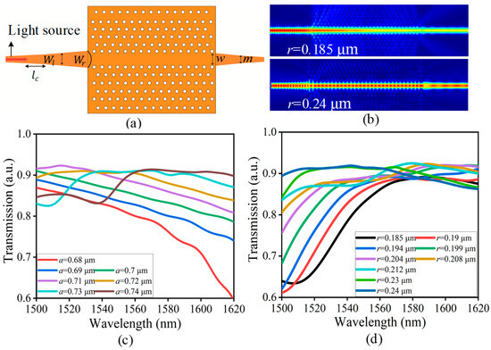
Figure 4.
Simulated transmission features of the designed 2D LN-based tapper waveguide integrated with a PhC waveguide: (a) the simulation model employed in this study; (b) the electric field distribution for each r; (c) the impact of a on the transmission efficiency; and (d) the effect of r on transmission efficiency. The transmission efficiency is plotted as a function of the wavelength, demonstrating the waveguide’s ability to guide and transmit light efficiently within the specified a and r.
This study investigates the impact of the middle-tapered section on the coupling between the two waveguides, specifically in the context of integrating LN into the slab and coupling it via a tapered waveguide. We examined the effects of the a and r on the transmission efficiency of a tapered waveguide integrated with a PhC waveguide. Initially, the widths of the tapered sections were set with at 1 μm and at 1.55 μm, with a fixed at 5 μm. Figure 4b illustrates the electric field distribution at a wavelength of 1550 nm, for r at 0.185 μm and 0.24 μm. Figure 4c shows the effect of varying a from 0.68 μm to 0.74 μm. The transmission efficiency decreases from 86% to 60% across the wavelength range 1500 nm to 1620 nm when a reaches 0.68 μm. Increasing a to 0.72 μm significantly improves performance, yielding efficiencies between 85% and 89% over the same range, with a peak of 90% within the C-band. Conversely, when a is fixed at 0.72 μm, and r is increased from 0.185 μm to 0.24 μm, further enhancements are observed, as shown in Figure 4d. At r = 0.185 μm, the transmission efficiency ranges from 62% to 87%. Increasing r to 0.24 μm stabilizes the transmission efficiency at between 86% and 88%, achieving a peak of 92% in the C-band. These findings underscore the significant influence of both a and r on the transmission efficiency of the integrated tapered waveguide and PhC waveguide system. Optimizing these parameters is critical for advancing high-performance photonic devices in optical communication applications.
Additionally, we investigate the influence of various taper conditions on waveguide transmission. The simulations are conducted with the following fixed parameters: z at 0.3 μm, a at 0.72 μm, r at 0.24 μm, and tapered waveguide widths of 1 μm and 1.55 μm on either side. The length of the tapered waveguide is set at 5 μm, and m is set at 0.3 μm, with a fixed inclination angle of 70°. Initially, as seen in Figure 5a, the width of the tapered waveguide is varied between 1 μm and 2 μm, and is fixed at 1.55 μm. When is set to 1 μm, the transmission efficiency ranges from 90% to 88%. When is increased to 2 μm, the transmission efficiency decreases, reaching values between 85% and 83%. Furthermore, with fixed at 1 μm, the width of the input part of the tapered waveguide is varied between 0.1 μm and 1.55 μm. The effects of these variations on transmission efficiency are illustrated in Figure 5b. With set at 0.1 μm, the transmission efficiency ranges from 33% to 49%. However, as increases to 1.55 μm, the transmission efficiency improves significantly, reaching values between 81% and 92%. These findings clearly demonstrate that wider tapered waveguides substantially enhance transmission efficiency, highlighting the importance of optimizing the waveguide geometry of high-performance photonic devices.
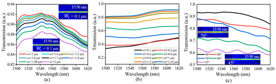
Figure 5.
Influence of the taper waveguide widths and inclination angle on the transmission efficiency of an LN-based taper integrated with PhC waveguides. (a,b) demonstrate the influence of the taper waveguide widths and , respectively, on the transmission efficiency. Furthermore, the electric field distribution also shows the fundamental mode for each . (c) shows the effect of the inclination angle on the transmission efficiency. The electric field distribution is also shown for each inclination angle.
The selection of the parameter ranges, specifically from 0.1 μm to 1.55 μm and from 1.0 μm to 2.0 μm, is strategically aimed at optimizing the performance of the taper waveguide. The narrower width range of exploits LN’s high refractive index, facilitating the strong subwavelength mode confinement essential for efficient light–matter interactions at extreme submicron scales. Conversely, the wider range of ensures compatibility with the periodicity of PhC structures while maintaining single-mode operation, which is crucial for avoiding the multimode effects prevalent in silicon devices at widths exceeding 700 nm. In LN, the high index contrast effectively suppresses higher-order modes, even up to 2.0 μm, as evidenced by the fundamental-mode electric field profiles which are illustrated in Figure 5a. Furthermore, recent advancements in nanofabrication techniques, including high-precision plasma etching and ion-slicing, have validated the feasibility of implementing these dimensions, allowing for ultra-compact photonic designs without sacrificing transmission efficiency, and thereby enhancing LN’s viability in next-generation photonic applications.
The influence of the inclination angle on transmission efficiency is illustrated in Figure 5c. As the inclination angle decreases from 90° to 45°, the maximum transmission efficiency declines significantly. This trend is evident in Figure 5c, in which the black curve corresponds to 90° and the purple curve represents 45°. Most efficiency curves exhibit a systematic downward shift as the inclination angle decreases. Notably, at 90°, the transmission efficiency ranges from 90% to 85%; in comparison, in the case of 45°, the transmission efficiency range decreases to between 59% and 45%. Further analysis, as shown in Figure 5c, compares the electric field distributions at 70° and 45° with a wavelength of 1550 nm, revealing a decrease in transmission efficiency from 73% to 59%. This reduction, evident in the diminished electric field intensity profiles, underscores the critical role of the inclination angle in governing optical performance. These findings emphasize the necessity of optimizing this parameter in photonic device design to ensure high-efficiency operation.
4. Influence of Inclination Angle on the High-Q 2D LN-Based PhC Optical Cavity
4.1. Design Guidelines
Figure 6a illustrates the integration of a high-Q 2D LN-based PhC optical cavity with tapered and PhC waveguides. The optical cavity structure was designed and analyzed using Lumerical 3D FDTD, which employs resonant mode analysis to compute the Q-factor. The cavity comprises a 50 × 32 array of air holes (columns × rows) to ensure robust photonic bandgap confinement. The simulation domain and boundary conditions (PML layers, adaptive meshing, and domain dimensions of 54 µm × 17 µm × 3 µm) remain consistent, following the methodology detailed in Section 3.2. The light source is positioned on the right side of the structure, enabling efficient coupling into the cavity. The figure also shows the line-defected PhC waveguide details, where an air slot is introduced at its center which is denoted by s, and where w represents the distance between the centers of adjacent air holes. Normally, w = k* √3 a; here, we select 1.2 as the value of k, so it can be determined that the value of w can be 1.2 μm; accordingly, we set a to 0.72 μm, and the s values can vary from 0.06 μm to 0.2 μm. Figure 6b shows a detailed view of the controlled geometric adjustments applied to the air-hole lattice to optimize the cavity’s PBG. The air holes are shifted by 0.005 µm, 0.01 µm, and 0.015 µm along the first, second, and third directions, respectively. These deliberate perturbations break the symmetry of the PhC lattice, localizing the optical mode within the cavity region and suppressing radiative losses. The strategic displacement of air holes is critical for achieving high Q-factor values, as it balances mode confinement with fabrication feasibility.
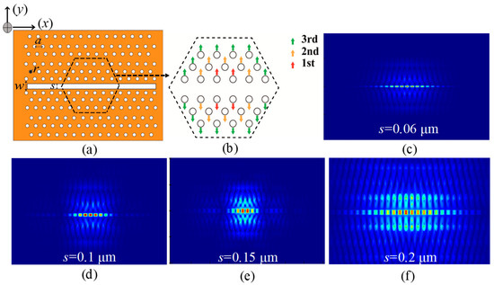
Figure 6.
Design principles and light confinement characteristics of the high-Q 2D LN-based PhC optical cavity. (a,b) illustrate the design principles of the high-Q 2D LN-based PhC optical cavity. Additionally, the calculated electric field distributions in the x–y plane are presented for varying slot widths: 0.06 μm (c), 0.1 μm (d), 0.15 μm (e), and 0.2 μm (f).
Figure 6c–f present the simulated electric field distributions in the x–y plane for four slot widths: 0.05 µm (c), 0.1 µm (d), 0.15 µm (e), and 0.2 µm (f). The results highlight the strong dependence of the electric field profile on the slot width (s). A narrower s, at 0.06 µm, exhibits intensified field localization within the cavity, owing to stronger light–matter interactions at the slot edges. In contrast, a wider s, at 0.2 µm, reduces field confinement, leading to broader mode profiles and diminished Q-factors. These findings underscore the necessity of precise geometric control in tailoring the optical performance of LN-based PhC cavities, particularly for applications requiring ultrahigh-Q resonances or enhanced nonlinear effects.
4.2. Influence of Inclination Angle on Optical Mode and Q-Factor
The properties of a 2D LN-based PhC optical cavity were examined using the Lumerical 3D FDTD method, which employs a resonant mode analysis method to find the Q-factor. Figure 7a illustrates the influence of the inclination angle and air slot width (s) on the optical mode wavelength. The analysis is conducted with fixed parameters: a at 0.72 μm, r at 0.24 μm, and z at 0.3 μm. Figure 7a illustrates the relationships between the optical mode wavelength and the inclination angles for varying values of s, ranging from 0.06 µm to 0.2 µm. When s is set at 0.06 μm, and the inclination angle is 90°, the optical mode wavelength is observed to be 1512.17 nm. As the inclination angle decreases to 60°, the optical mode wavelength shifts to 1427.31 nm, demonstrating a significant shift of approximately 84.86 nm. Similarly, a smaller change in the inclination angle, from 90° to 85°, results in a shift of the optical mode wavelength from 1512.17 nm to 1482.76 nm. Conversely, when the inclination angle is fixed at 90° and s is increased from 0.06 µm to 0.2 µm, the optical mode wavelength shifts from 1512.17 nm to 1617.24 nm, corresponding to a total shift of 105.07 nm. Notably, even a single transition of s from 0.06 µm to 0.08 µm causes the optical mode wavelength to shift from 1512.17 nm to 1530.27 nm. Furthermore, when we set s at 0.14 μm and the inclination angle is 90°, the optical mode is exhibited at 1586.12 nm. Upon decreasing the inclination angle to 70°, the optical mode shifts to 1525.44 nm. These results underscore the significant influence of both the inclination angle and air slot width (s) on the optical mode wavelength, highlighting their critical roles in the design and optimization of photonic devices.
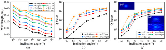
Figure 7.
Influence of inclination angle and air slot width on optical mode wavelength and Q-factor in 2D LN-based photonic crystal cavities. (a) Optical mode wavelength as a function of inclination angle for varying air slot widths (s) between 0.06 µm and 0.2 µm. (b) Q-factor dependence on inclination angle, with a varying from 0.69 µm to 0.72 µm. (c) Q-factor dependence on inclination angle, with r varying from 0.2 µm to 0.24 µm.
Figure 7b reveals a wide range of Q-factors, spanning from 1.213 × 10⁵ to 2.11 × 10⁷ in relation to the inclination angle, which varies from 90° to 60°. We kept a at 0.72 µm, r at 0.24 µm, and s at 0.14 µm. Initially, when the inclination angle was set at 90°, the Q-factor was determined to be 2.11 × 10⁷; this was accompanied by an optical mode wavelength of 1586.12 nm. Decreasing the inclination angle to 85° resulted in a Q-factor of 1.71 × 10⁷. Upon further decreasing the inclination angle to 70°, it exhibited a Q-factor of 6.21 × 10⁶, accompanied by an optical mode wavelength of 1525.44 nm. As the inclination angle decreases to 60°, the Q-factor significantly decreases, reaching a value of 1.213 × 10⁵. These results also demonstrate the strong dependence of the Q-factor on the inclination angle, highlighting its critical role in optimizing the performance of 2D LN-based optical cavities. The lowest Q-factor was due to suboptimal mode confinement and increased scattering losses, which disrupted the balance between the photonic bandgap and the defect mode overlap in the PhC cavity. Notably, the Q-factor drops sharply at a tilt angle of 75°. This degradation likely stems from excessive sidewall tilting, which reduces the effective bottom radius of the air holes. The diminished radius disrupts photonic bandgap confinement, enabling light to propagate from deeper within the holes, and increasing radiative losses through the substrate. This strong angular dependence of Q-factor corroborates our broader analysis of structural parameter trade-offs, in which the interplay of a, r, and inclination angle dictates the balance between mode confinement and loss suppression.
Our systematic investigation reveals that the optical Q-factor of 2D LN-based PhC optical cavity is critically governed by the interplay of a, r, and inclination angle. For a fixed cavity thickness z of 0.3 µm, reducing a from 0.72 µm to 0.69 µm induces a nonlinear degradation of Q-factors across all inclination angles from 90° to 60°, with the most pronounced collapse observed at shallow angles (e.g., 60°) (Figure 7b,c). With a at 0.69 µm, Q-factors plummet to <104 for 60°, a consequence of the geometric mismatch between the tapered waveguide and the PhC lattice. Parallel trends emerge when scaling the r. Reducing r from 24 µm to 0.2 µm progressively weakens the photonic bandgap, amplifying radiative losses and scattering-induced dissipation at low inclination angles, as shown in Figure 6c. For example, with r at 0.2 µm and 60°, Q-factors drop to 2 × 10⁴, approaching the threshold of operational viability.
Optimal performance, with a Q-factor of >106 for 70°, is achieved within the following defined parameter bounds: a at 0.72 µm and r at 240 µm. These ranges strike a balance between mode confinement governed by a and r and loss suppression sensitive to inclination angle-dependent geometric asymmetry. Deviations beyond these limits disrupt the bandgap-mediated light trapping, exposing the cavity to forms of fabrication-induced disorder like sidewall roughness and hole ellipticity. Our findings underscore that preserving high-Q operation in LN PhC cavities demands not only precise control of a and r but also strict angular alignment inclination angle ≥ 70° to mitigate scattering losses, a critical consideration for scalable integrated photonic systems.
Table 2 systematically compares the optical Q-factor of LN-based PhC cavities for inclination angles between 90° and 60°. While varying a = 0.72 µm to 0.69 µm, the Q-factor range also deteriorates nonlinearly, dropping from 2.11 × –1.21 × to 5.0 × –1.0 × . Similarly, when a is fixed at 0.72 and r is varied from 0.23 to 0.2 with inclination angles from 90° to 60°, the Q-factor range also deteriorates nonlinearly, dropping from 1.8 × –9.5 × to 8.0 × –2 × , with sharper declines at shallow inclination angles (≤70). These trends highlight a = 0.72 µm as the optimal design point, balancing broad C-band compatibility (1502–1581 nm), high transmission (90%), and superior Q-factors, factors which are critical for practical integrated photonic applications.
Table 2.
Variation of the Q-factor with respect to parameters a and r for different inclination angles between 90° and 60°. The table highlights the sensitivity of the Q-factor to the structural dimensions in the studied system.
Table 3 systematically compares the optical performance of LN-based PhC cavities across the range of varying a = 0.72 µm to 0.69 µm. As a decreases, the working wavelength range shifts toward shorter wavelengths and narrows, transitioning from 1502–1581 nm to 1372–1598 nm, indicating a compression of the photonic bandgap. Concurrently, C-band transmission efficiency declines from 90% to 82%, reflecting increased scattering losses at smaller lattice constants. On the other hand, when we fixed a at 0.72 µm and decreased r from 0.23 µm to 0.2 µm, the working wavelength range shifted toward shorter wavelengths and narrowed, transitioning from 1480–1575 nm to 1410–1575 nm, indicating a compression of the photonic bandgap. Concurrently, C-band transmission efficiency declined from 91% to 88%.
Table 3.
Performance metrics of LN-based PhC cavities as a function of a and r, including working wavelength range and C-band transmission efficiency, for an inclination angle of 70°.
The integration of tapered waveguides with PhC cavities enabled efficient light coupling and transmission, with transmission efficiencies exceeding 90% under optimized conditions. The Q-factor of our device surpasses those reported in Refs. [30,31,55,56,57] and is lower than that in Ref [58]. The Q-factor of the proposed LN-based device is particularly advantageous for applications in high-quality sensors [59] and optomechanical coupling. For nonlinear processes, a higher Q/V ratio enhances nonlinear conversion efficiency [60], while for LN-based temperature or electric field sensors, a higher Q-factor directly improves the figure of merit (FOM) [61]. Such high-Q LN cavities hold promise for applications like enhanced nonlinear optics or high-sensitivity sensing, complementing ongoing advancements in high-performance integrated photodetectors and sensors developed on silicon and germanium platforms [62,63,64,65].
Fabricating high-Q LN-based PhC cavities demands extreme precision: even nanoscale deviations degrade performance (Table 4). For optimal Q-factors > , a must exceed 0.72 µm. Reducing a to 0.69 µm triggers a nonlinear Q-factor collapse < from under-coupled modes and bandgap misalignment, necessitating that a be controlled within ±0.005 µm. Similarly, r must stay above 0.22 µm to sustain bandgap confinement; at r = 0.20 µm, Q-factors plummet to 2 × , necessitating an etching accuracy within ±0.01 µm. Inclination angles < 70° induce severe scattering losses, collapsing Q-factors by 100× and requiring alignment within ±2° for symmetric modes. Air slot width (s) variations shift optical modes to shorter wavelengths and reduce transmission, demanding careful coordination with inclination angles to minimize geometric mismatch. To sustain high Q > and C-band compatibility (1502–1581 nm), advanced techniques like electron-beam lithography and anisotropic etching are essential, as the degree of geometric perfection governs losses and spectral alignment. These tolerances highlight the intricate link between design and fabrication, posing challenges for the scaling of LN-based cavities into practical photonic systems.
Table 4.
Comparison of the theoretical optical high-Q factors for different optical cavities or structures.
5. Discussion
This study acknowledges inherent limitations in its computational methodology used for modeling the integrated taper PhC waveguide system. The hybrid 2.5D varFDTD framework, while computationally efficient for simulating longitudinally invariant structures, imposes critical simplifications when applied to the tapered waveguide–PhC interface. By assuming uniformity along the vertical axis (z-invariance), the model neglects three-dimensional mode reshaping and out-of-plane scattering effects at the inclined coupling interface. Furthermore, the framework does not account for fabrication-induced sidewall angle variations or etch-depth nonuniformity, which are known to perturb the photonic bandgap and degrade cavity Q-factors in experimental implementations. While parameter ranges (inclination angles: 90–60°, a and r, , ) were constrained to experimentally achievable values to ensure practical relevance, this approach excludes extreme geometric deviations that could reveal fundamental trade-offs between mode confinement and fabrication tolerances. These simplifications highlight a critical gap in modeling dynamic, process-dependent defects (e.g., resist reflow or plasma-induced roughness) that evolve during fabrication. To resolve these limitations, future work will transition to full 3D multiphysics simulations, enabling the coupled optical–mechanical analysis of defect propagation and its impact on taper–PhC coupling efficiency across broader parameter spaces.
Achieving ultrahigh Q-factors > in LN-based PhC cavities necessitates careful balancing of optical performance against structural robustness and fabrication feasibility. While narrow air slots of 0.14 µm and steep inclination angles of 90–60° enhance optical confinement, they also amplify mechanical fragility and etching challenges. For instance, sub-100 nm slot widths increase susceptibility to stress-induced fractures during ICP etching, while aggressive angles exacerbate sidewall roughness due to ion flux shadowing (Figure 1f). To mitigate these trade-offs, our design prioritized slot widths of 0.1 µm and moderate inclination angles (70–72°), accepting a marginal Q-factor reduction to improve yield and structural integrity. Future iterations will integrate stress-relief nanostructures, such as tapered supports or strain-gradient architectures, to decouple optical performance from mechanical vulnerability, thereby preserving high Q-factors while maintaining fabrication resilience. The future work could explore AI-driven modeling [66,67] for these purposes.
6. Conclusions
We analyzed the fabrication-induced imperfections of a 2D LN-based PhC cavity sample with a 70° inclination angle, including nonuniform feature sizes, edge-profile irregularities, nanoscale voids, and incomplete etching, which collectively highlight the critical influence of nanofabrication tolerances on LN-based device performance. Subsequently, we systematically optimized key structural parameters, including a, r, z, and inclination angle. We achieved a narrow-bandgap PhC structure operating in the wavelength range of 1531–1606 nm, with a high transmission efficiency of 93%. Furthermore, we investigated the influence of the inclination angle on the optical mode wavelength and Q-factor, revealing the strong dependence of these performance metrics on geometric design. Remarkably, we achieved an exceptional Q-factor of up to 6.21 × 10⁶ at an inclination angle of 70°, underscoring the critical role of inclination angle optimization in maximizing device performance. The combination of a narrow photonic bandgap and ultrahigh Q-factor proves particularly advantageous for micro-electromechanical systems (MEMS) and high-precision accelerometer devices, applications in which spectral selectivity and minimal energy dissipation are critical for enhanced sensitivity and measurement accuracy.
Author Contributions
Conceptualization, S.M. and Y.H.; methodology, S.M.; software, S.M.; validation, D.C., J.Z. and Z.L.; investigation, S.M. and C.X.; writing—original draft preparation, S.M. and B.F.; writing—review and editing, S.M., P.K., B.F., L.M. and Y.H.; supervision, G.W. All authors have read and agreed to the published version of the manuscript.
Funding
This work was supported in part by the National Natural Science Foundation of China (project contract nos. 62371106, U2230206, and 62204264), in part by the National Key R&D Program (project contract no. 2022YFA1405900), in part by the Sichuan Provincial Science and Technology Planning Program (project contract nos. 2022YFG0230 and 2023YFG0040), in part by the Joint Fund of ZF and the Ministry of Education (grant no. 8091B022126), in part by the Fundamental Enhancement Program Technology Area Fund (grant no. 2021-JCJQ-JJ-0667), in part by the China Postdoctoral Science Foundation (project contract no. 2023M740534), and in part by the Innovation Ability Construction Project for Sichuan Provincial Engineering Research Center of Communication Technology for Intelligent IoT (2303-510109-04-03-318020).
Institutional Review Board Statement
Not applicable.
Informed Consent Statement
Not applicable.
Data Availability Statement
The original contributions presented in this study are included in the article. Further inquiries can be directed to the corresponding authors.
Conflicts of Interest
Authors Jun Zhou and Zhongke Lei were employed by the company Sichuan Guoruan Technology Group Co., Ltd. The remaining authors declare that the research was conducted in the absence of any commercial or financial relationships that could be construed as a potential conflict of interest.
References
- Nozaki, K.; Tanabe, T.; Shinya, A.; Matsuo, S.; Sato, T.; Taniyama, H.; Notomi, M. Sub-femtojoule all-optical switching using a photonic-crystal nanocavity. Nat. Photonics 2010, 4, 477. [Google Scholar] [CrossRef]
- Kuramochi, E.; Nozaki, K.; Shinya, A.; Takeda, K.; Sato, T.; Matsuo, S.; Taniyama, H.; Sumikura, H.; Notomi, M. Large-scale integration of wavelength-addressable all-optical memories on a photonic crystal chip. Nat. Photonics 2014, 8, 474. [Google Scholar] [CrossRef]
- Fan, X.; White, I.M.; Shopova, S.I.; Zhu, H.; Suter, J.D.; Sun, Y. Sensitive optical biosensors for unlabeled targets. Anal. Chim. Acta 2008, 620, 8. [Google Scholar] [CrossRef] [PubMed]
- Soljacic, M.; Joannopoulos, J.D. Enhancement of nonlinear effects using photonic crystals. Nat. Mater. 2004, 3, 211. [Google Scholar] [CrossRef] [PubMed]
- Lodahl, P.; Mahmoodian, S.; Stobbe, S. Interfacing single photons and single quantum dots with photonic nanostructures. Rev. Mod. Phys. 2015, 87, 347. [Google Scholar] [CrossRef]
- Song, B.-S.; Noda, S.; Asano, T.; Akahane, Y. Ultra-high-Q photonic crystal nanocavities realized by the local width modulation of a line defect. Nat. Mater. 2005, 4, 207. [Google Scholar] [CrossRef]
- Noda, S.; Fujita, M.; Asano, T. Spontaneous-emission control by photonic crystals and nanocavities. Nat. Photonics 2007, 1, 449, 1800228 (7 of 8) www.lpr-journal.org. [Google Scholar] [CrossRef]
- Combrie, S.; De Rossi, A.; Tran, Q.V.; Benisty, H. GaInP photonic crystal cavity with ultra-high Q-factor. Opt. Lett. 2008, 33, 1908. [Google Scholar] [CrossRef]
- Eggleton, B.J.; Luther-Davies, B.; Richardson, K. Chalcogenide photonics. Nat. Photonics 2011, 5, 141. [Google Scholar] [CrossRef]
- Trivino, N.V.; Minkov, M.; Urbinati, G.; Galli, M.; Carlin, J.-F.; Butte, R.; Savona, V.; Grandjean, N. III-nitride photonic crystal light-emitting diodes with high extraction efficiency. Appl. Phys. Lett. 2014, 105, 231119. [Google Scholar]
- Debnath, K.; Clementi, M.; Bucio, T.D.; Khokhar, A.Z.; Sotto, M.; Grabska, K.M.; Bajoni, D.; Galli, M.; Saito, S.; Gardes, F.Y. High-speed silicon optical modulator based on a photonic crystal waveguide. Opt. Express 2017, 25, 27334. [Google Scholar] [CrossRef] [PubMed]
- Kosters, M.; Sturman, B.; Werheit, P.; Haertle, D.; Buse, K. Optical tunability of photonic crystal cavities infiltrated with liquid crystals. Nat. Photonics 2009, 3, 510. [Google Scholar]
- Weis, R.S.; Gaylord, T.K. Lithium niobate: Summary of physical properties and crystal structure. Appl. Phys. A 1985, 37, 191. [Google Scholar] [CrossRef]
- Wooten, E.L.; Kissa, K.M.; Yi-Yan, A.; Murphy, E.J.; Lafaw, D.A.; Hallemeier, P.F.; Maack, D.; Attanasio, D.V.; Fritz, D.J.; McBrien, G.J.; et al. A review of lithium niobate modulators for fiber-optic communications systems. IEEE J. Sel. Top. Quantum Electron. 2000, 6, 69–82. [Google Scholar] [CrossRef]
- Myers, L.E.; Eckardt, R.C.; Fejer, M.M.; Byer, R.L.; Bosenberg, W.R.; Pierce, J.W. Quasi-phase-matched optical parametric oscillators in bulk periodically poled LiNbO3. J. Opt. Soc. Am. B 1995, 12, 2102–2116. [Google Scholar] [CrossRef]
- Halder, M.; Beberatos, A.; Gisin, N.; Scarani, V.; Simon, C.; Zbinden, H. Entangling independent photons by time measurement. Nat. Phys. 2007, 3, 692–695. [Google Scholar] [CrossRef]
- Pijolat, M.; Loubriat, S.; Queste, S.; Mercier, D.; Reinhardt, A.; Defay, E.; Deguet, C.; Clavelier, L.; Moriceau, H.; Aid, M.; et al. Large electromechanical coupling factor film bulk acoustic resonator with X-cut LiNbO3 layer transfer. Appl. Phys. Lett. 2009, 95, 182106. [Google Scholar] [CrossRef]
- Gong, S.; Piazza, G. Design and analysis of lithium-niobate-based high electromechanical coupling RF-MEMS resonators for wideband filtering. IEEE Trans. Microw. Theory Tech. 2013, 61, 403–414. [Google Scholar] [CrossRef]
- Heanue, J.F.; Bashaw, M.C.; Hesselink, L. Volume holographic storage and retrieval of digital data. Science 1994, 265, 749–752. [Google Scholar] [CrossRef]
- Buse, K.; Adibi, A.; Psaltis, D. Non-volatile holographic storage in doubly doped lithium niobate crystals. Nature 1998, 393, 665–668. [Google Scholar] [CrossRef]
- Reindl, L.M.; Shrena, I.M. Wireless measurement of temperature using surface acoustic waves sensors. IEEE Trans. Ultrason. Ferroelectr. Freq. Control 2004, 51, 1457–1463. [Google Scholar] [CrossRef] [PubMed]
- Arizmendi, L. Photonic applications of lithium niobate crystals. Phys. Status Solidi A 2004, 201, 253–283. [Google Scholar] [CrossRef]
- Notomi, M.; Kuramochi, E.; Tanabe, T. High-Q Photonic Crystal Nanocavities in Silicon-on-Insulator. Nat. Photonics 2008, 2, 741–747. [Google Scholar] [CrossRef]
- Upham, J.; Tanaka, Y.; Asano, T.; Noda, S. Fabrication and Characterization of High-Q Silicon Photonic Crystal Cavities. Optica 2017, 4, 140–144. [Google Scholar]
- Guarino, A.; Poberaj, G.; Rezzonico, D.; Günter, P. Electro–optically tunable microring resonators in lithium niobate. Nat. Photonics 2007, 1, 407–410. [Google Scholar] [CrossRef]
- Rabiei, P.; Ma, J.; Khan, S.; Chiles, J.; Fathpour, S. Heterogeneous lithium niobate photonics on silicon substrates. Opt. Express 2013, 21, 25573–25581. [Google Scholar] [CrossRef]
- Chen, D.; Muhammad, S.; Huang, W.; Zheng, X.; Wen, G.; Huang, Y. Parameter investigations on lithium-niobate-based photonic crystal optomechanical cavity. Results Phys. 2023, 48, 106458. [Google Scholar] [CrossRef]
- Lu, J.; Zhou, S.; Wu, Y.; Yu, H. Two-dimensional thin film lithium niobate photonic crystal waveguide for integrated photonic chips. Appl. Phys. Lett. 2024, 124, 141104. [Google Scholar] [CrossRef]
- Liang, H.; Luo, R.; He, Y.; Jiang, H.; Lin, Q. High-quality lithium niobate photonic crystal nanocavities. Optica 2017, 4, 1251–1258. [Google Scholar] [CrossRef]
- Li, M.; Liang, H.; Luo, R.; He, Y.; Lin, Q. High-Q 2D Lithium Niobate Photonic Crystal Slab Nanoresonators. Laser Photonics Rev. 2019, 13, 1800228. [Google Scholar] [CrossRef]
- Ge, R.; Yan, X.; Liang, Z.; Li, H.; Wu, J.; Liu, X.; Chen, Y.; Chen, X. Large quality factor enhancement based on cascaded uniform lithium niobate bichromatic photonic crystal cavities. Opt. Lett. 2022, 48, 113–116. [Google Scholar] [CrossRef]
- Lin, J.; Xu, Y.; Fang, Z.; Wang, M.; Song, J.; Wang, N.; Qiao, L.; Fang, W.; Cheng, Y. Fabrication of high-Q lithium niobate microresonators using femtosecond laser micromachining. Sci. Rep. 2015, 5, 8072. [Google Scholar] [CrossRef] [PubMed]
- Li, S.; Cai, L.; Wang, Y.; Jiang, Y.; Hu, H. Waveguides consisting of single-crystal lithium niobate thin film and oxidized titanium stripe. Opt. Express 2015, 23, 24212–24219. [Google Scholar] [CrossRef] [PubMed]
- Weigel, P.; Savanier, M.; DeRose, C.; Pomerene, A.T.; Starbuck, A.L.; Lentine, A.L.; Stenger, V.; Mookherjea, S. Lightwave Circuits in Lithium Niobate through Hybrid Waveguides with Silicon Photonics. Sci. Rep. 2016, 6, 22301. [Google Scholar] [CrossRef]
- Witmer, J.D.; Valery, J.A.; Arrangoiz-Arriola, P.; Sarabalis, C.J.; Hill, J.T.; Safavi-Naeini, A.H. High-Q photonic resonators and electro-optic coupling using silicon-on-lithium-niobate. Sci. Rep. 2017, 7, 46313. [Google Scholar] [CrossRef] [PubMed] [PubMed Central]
- Diziain, S.; Geiss, R.; Steinert, M.; Schmidt, C.; Chang, W.-K.; Fasold, S.; Füßel, D.; Chen, Y.-H.; Pertsch, T. Self-suspended micro-resonators patterned in Z-cut lithium niobate membranes. Opt. Mater. Express 2015, 5, 2081–2089. [Google Scholar] [CrossRef]
- Lu, H.; Baida, F.I.; Ulliac, G.; Courjal, N.; Collet, M.; Bernal, M.-P. Lithium niobate photonic crystal wire cavity: Realization of a compact electro-optically tunable filter. Appl. Phys. Lett. 2012, 101, 151117. [Google Scholar] [CrossRef]
- Zhou, G.; Gu, M. Direct optical fabrication of three-dimensional photonic crystals in a high refractive index LiNbO3 crystal. Opt. Lett. 2006, 31, 2783–2785. [Google Scholar] [CrossRef]
- Roussey, M.; Bernal, M.-P.; Courjal, N.; van Labeke, D.; Baida, F.I.; Salut, R. Electro-optic effect exaltation on lithium niobate photonic crystals due to slow photons. Appl. Phys. Lett. 2006, 89, 241110. [Google Scholar] [CrossRef]
- Geiss, R.; Diziain, S.; Iliew, R.; Etrich, C.; Hartung, H.; Janunts, N.; Schrempel, F.; Lederer, F.; Pertsch, T.; Kley, E.-B. Light propagation in a free-standing lithium niobate photonic crystal waveguide. Appl. Phys. Lett. 2010, 97, 131109. [Google Scholar] [CrossRef]
- Jiang, W.; Lin, Q. Chip-scale cavity optomechanics in lithium niobate. Sci. Rep. 2016, 6, 36920. [Google Scholar] [CrossRef]
- Wang, C.; Xiong, X.; Andrade, N.; Venkataraman, V.; Ren, X.-F.; Guo, G.-C.; Loncar, M. Second harmonic generation in lithium niobate microdisk resonators. Opt. Express 2017, 25, 6963. [Google Scholar] [CrossRef]
- Krasnokutska, I.; Chapman, R.J.; Tambasco, J.-L.J.; Peruzzo, A. High coupling efficiency grating couplers on lithium niobate on insulator. Opt. Express 2019, 27, 17681–17685. [Google Scholar] [CrossRef] [PubMed]
- Baba, T. Photonic Integration Based on Si Photonics and Photonic Crystals. In Proceedings of the 2021 Opto-Electronics and Communications Conference (OECC), Hong Kong, China, 3–7 July 2021; pp. 1–3. [Google Scholar]
- Jokar, M.H.; Naraghi, A.; Seifouri, M.; Olyaee, S. Design of bio-alcohol sensor based on waveguide-coupled photonic crystal cavity. Results Opt. 2023, 13, 100563. [Google Scholar] [CrossRef]
- Shekhar, S.; Bogaerts, W.; Chrostowski, L.; Bowers, J.E.; Hochberg, M.; Soref, R.; Shastri, B.J. Roadmapping the next generation of silicon photonics. Nat. Commun. 2024, 15, 751. [Google Scholar] [CrossRef] [PubMed]
- Krauss, T.F. Slow light in photonic crystal waveguides. J. Phys. D Appl. Phys. 2007, 40, 2666. [Google Scholar] [CrossRef]
- Baba, T. Slow light in photonic crystals. Nat. Photonics 2008, 2, 465–473. [Google Scholar] [CrossRef]
- Notomi, M.; Kuramochi, E.; Taniyama, H. Ultrahigh-Q nanocavity with 1D photonic gap. Opt. Express 2008, 16, 11095–11102. [Google Scholar] [CrossRef]
- O’brien, J.L.; Furusawa, A.; Vučković, J. Photonic quantum technologies. Nat. Photonics 2009, 3, 687–695. [Google Scholar] [CrossRef]
- Elsherif, M.; Salih, A.E.; Muñoz, M.G.; Alam, F.; AlQattan, B.; Antonysamy, D.S.; Zaki, M.F.; Yetisen, A.K.; Park, S.; Wilkinson, T.D.; et al. Optical fiber sensors: Working principle, applications, and limitations. Adv. Photonics Res. 2022, 3, 2100371. [Google Scholar] [CrossRef]
- Shen, B.; Hu, D.; Dai, C.; Yu, X.; Tan, X.; Sun, J.; Jiang, J.; Jiang, A. Advanced Etching Techniques of LiNbO3 Nanodevic-es. Nanomaterials 2023, 13, 2789. [Google Scholar] [CrossRef]
- Yang, Y.-H.; Xu, X.-B.; Wang, J.-Q.; Zhang, M.; Li, M.; Zhu, Z.-X.; Wang, Z.-B.; Dong, C.-H.; Fang, W.; Yu, H.; et al. Nonlinear Optical Radiation of a Lithium Niobate Microcavity. Phys. Rev. Appl. 2023, 19, 034087. [Google Scholar] [CrossRef]
- Shugayev, R.; Dominguez, D.; Leenheer, A.; Little, B.; Chow, M.N.H.; Karl, N.; Koppa, M.; Gehl, M.; Jau, Y.-Y.; Eichenfield, M. CMOS-Fabricated Ultraviolet Light Modulators Using Low-Loss Alumina Piezo-Optomechanical Photonic Circuits. Opt. Express 2023, 31, 7890–7898. [Google Scholar]
- Yamamoto, T.; Notomi, M.; Taniyama, H.; Kuramochi, E.; Yoshikawa, Y.; Torii, Y.; Kuga, T. Design of a high-Q air-slot cavity based on a width-modulated line-defect in a photonic crystal slab. Opt. Express 2008, 16, 13809–13817. [Google Scholar] [CrossRef]
- Li, Y.; Zheng, J.; Gao, J.; Shu, J.; Aras, M.S.; Wong, C.W. Design of dispersive optomechanical coupling and cooling in ultrahigh Q/Vslot-type photonic crystal cavities. Opt. Express 2010, 18, 23844–23856. [Google Scholar] [CrossRef] [PubMed]
- Dharanipathy, U.P.; Minkov, M.; Tonin, M.; Savona, V.; Houdré, R. High-Q silicon photonic crystal cavity for enhanced optical nonlinearities. Appl. Phys. Lett. 2014, 105, 101101. [Google Scholar] [CrossRef]
- Muhammad, S.; Chen, D.; Xian, C.; Zhou, J.; Lei, Z.; Kuang, P.; Li, Z.; Wen, G.; Huang, Y. Design and Fabrication of High-Quality Two-Dimensional Silicon-Based Photonic Crystal Optical Cavity with Integrated Waveguides. Photonics 2024, 11, 753. [Google Scholar] [CrossRef]
- Lee, W.-B.; Kwon, Y.-J.; Kim, A.; Sunwoo, Y.-H.; Lee, S.-S. Hybrid integrated thin-film lithium niobate–silicon nitride electro-optical phased array incorporating silicon nitride grating antenna for two-dimensional beam steering. Opt. Express 2024, 32, 9171–9183. [Google Scholar] [CrossRef]
- Li, M.; Ling, J.; He, Y.; Javid, U.A.; Xue, S.; Lin, Q. Lithium niobate photonic-crystal electro-optic modulator. Nat. Commun. 2020, 11, 4123. [Google Scholar] [CrossRef]
- Li, Y.; Wang, C.; Loncar, M. Design of nano-groove photonic crystal cavities in lithium niobate. Opt. Lett. 2015, 40, 2902–2905. [Google Scholar] [CrossRef]
- Lotfiani, A.; Dehdashti Jahromi, H.; Hamedi, S. Monolithic silicon-based photovoltaic-nanoplasmonic biosensor with enhanced limit of detection and minimum detectable power. J. Light. Technol. 2022, 40, 1231–1237. [Google Scholar] [CrossRef]
- Dehdashti Jahromi, H.; Lotfiani, A. A fast and sensitive Schottky photodiode with surface plasmon enhanced photocurrent and extremely low dark current for high-frequency applications in near-infrared. IEEE Sens. J. 2022, 22, 20430–20437. [Google Scholar] [CrossRef]
- Lotfiani, A.; Jahromi, H.D. Guided-mode resonance enhanced Ge-on-Si self-powered surface illuminated photodetector for ultrahigh-speed optical communication systems. IEEE Sens. J. 2024, 24, 40669–40677. [Google Scholar] [CrossRef]
- Dehdashti Jahrom, H. Germanium-incorporated Si-Ge-Si heterojunction phototransistors for a high-limit of detection and wide linear dynamic range near-infrared light detection. Opt. Express 2024, 32, 43475–43489. [Google Scholar] [CrossRef]
- Yüksel, N.; Börklü, H.R.; Sezer, H.K.; Canyurt, O.E. Review of artificial intelligence applications in engineering design perspective. Eng. Appl. Artif. Intell. 2023, 118, 105697. [Google Scholar] [CrossRef]
- Jahromi, H.D.; Hamedi, S. Artificial intelligence approach for calculating electronic and optical properties of nanocomposites. Mater. Res. Bull. 2021, 141, 111371. [Google Scholar] [CrossRef]
Disclaimer/Publisher’s Note: The statements, opinions and data contained in all publications are solely those of the individual author(s) and contributor(s) and not of MDPI and/or the editor(s). MDPI and/or the editor(s) disclaim responsibility for any injury to people or property resulting from any ideas, methods, instructions or products referred to in the content. |
© 2025 by the authors. Licensee MDPI, Basel, Switzerland. This article is an open access article distributed under the terms and conditions of the Creative Commons Attribution (CC BY) license (https://creativecommons.org/licenses/by/4.0/).