High Absorption Broadband Ultra-Long Infrared Absorption Device Based on Nanoring–Nanowire Metasurface Structure

 ,
,  ,
,  ,
, 
Abstract
1. Introduction
2. Models and Methods
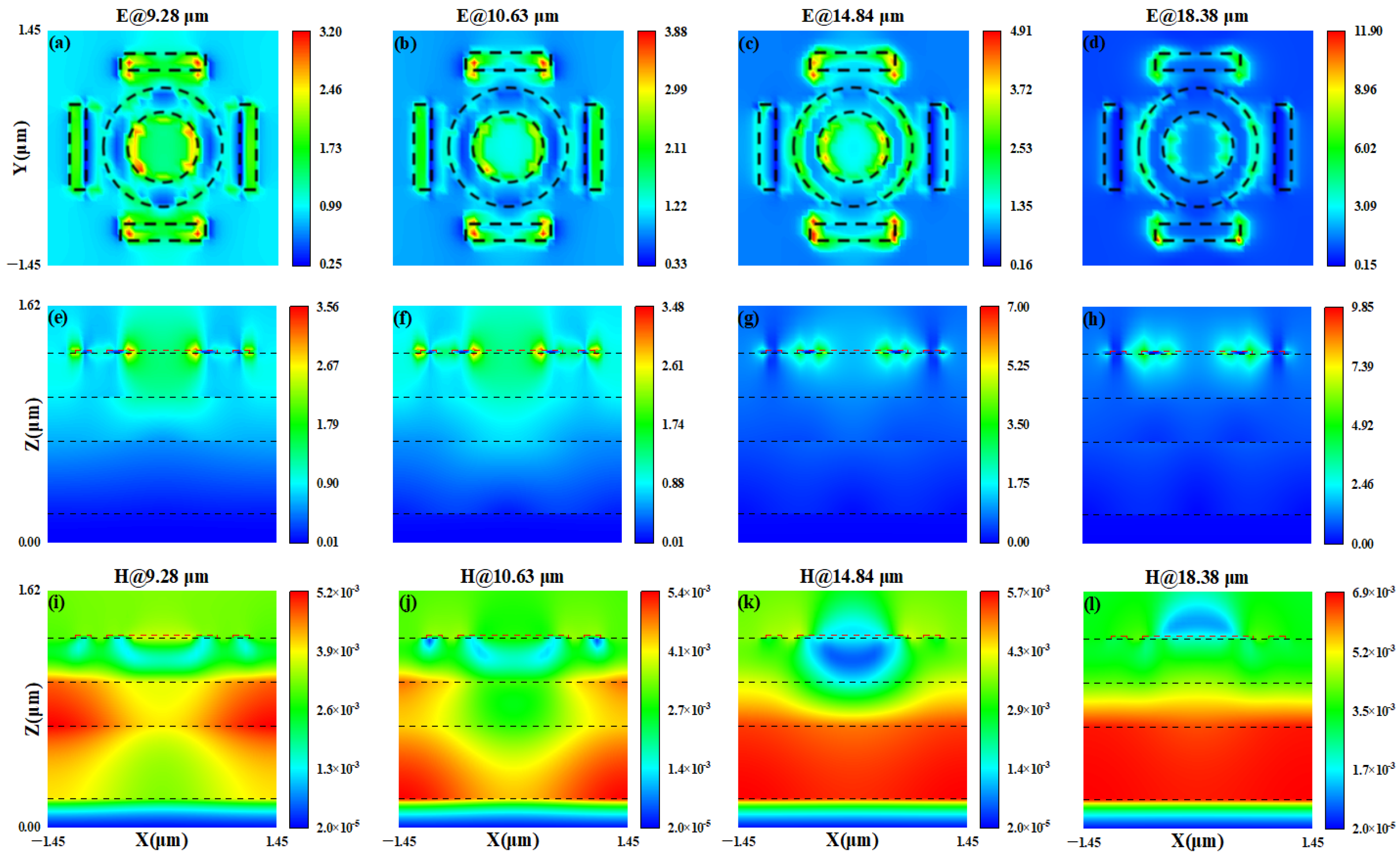
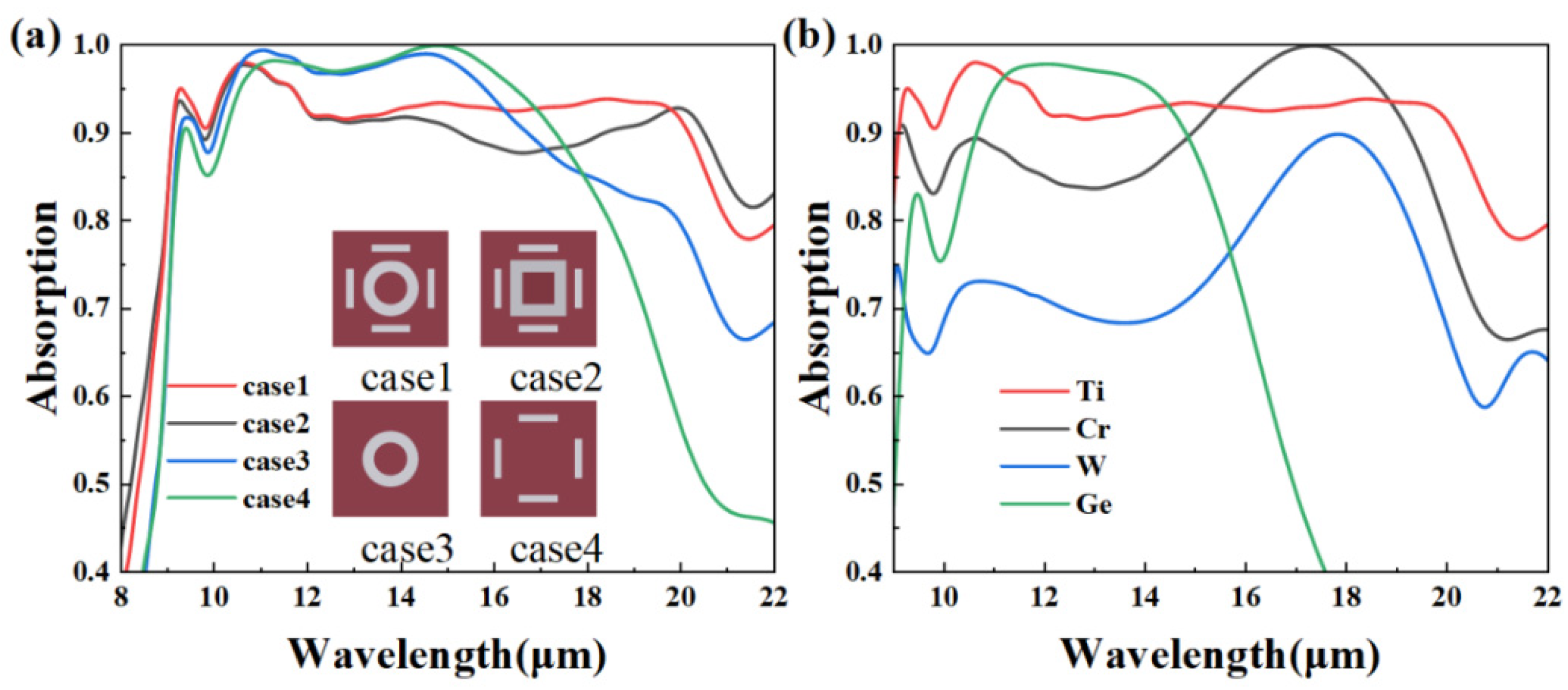
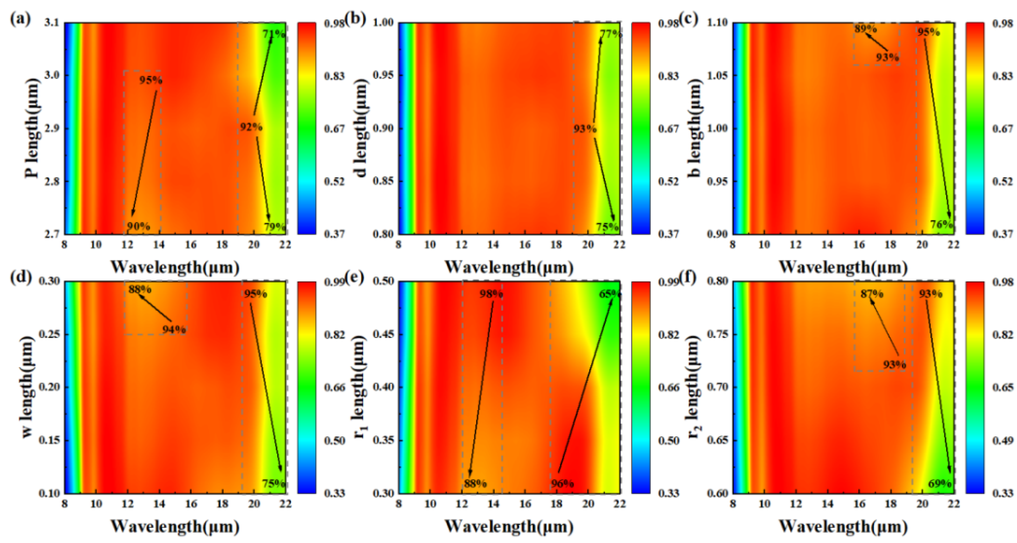
3. Results and Discussion
4. Conclusions
Author Contributions
Funding
Institutional Review Board Statement
Informed Consent Statement
Data Availability Statement
Conflicts of Interest
References
- Berhe, A.M.; As’ham, K.; Al-Ani, I.; Hattori, H.T.; Miroshnichenko, A.E. Strong coupling and catenary field enhancement in the hybrid plasmonic metamaterial cavity and TMDC monolayers. Opto-Electron. Adv. 2024, 7, 230181. [Google Scholar] [CrossRef]
- Zeng, Y.; Ling, Z.X.; Liu, G.D.; Wang, L.L.; Lin, Q. Tunable plasmonically induced transparency with giant group delay in gain-assisted graphene metamaterials. Opt. Express 2022, 30, 455954. [Google Scholar] [CrossRef]
- Yu, Z.; Li, M.; Xing, Z.; Gao, H.; Liu, Z.; Pu, S.; Mao, H.; Cai, H.; Ma, Q.; Ren, W.; et al. Genetic algorithm assisted meta-atom design for high-performance metasurface optics. Opto-Electron. Sci. 2024, 3, 240016. [Google Scholar] [CrossRef]
- Zhang, B.W.; Luo, Y.N. Dynamic optical tuning and sensing in L-shaped dirac semimetal-based terahertz metasurfaces. Phys. Lett. A 2025, 541, 130419. [Google Scholar] [CrossRef]
- Sande, S.I.; Deng, Y.; Bozhevolnyi, S.I.; Ding, F. Spin-controlled generation of a complete polarization set with randomly-interleaved plasmonic metasurfaces. Opto-Electron. Adv. 2024, 7, 240076. [Google Scholar] [CrossRef]
- Li, W.X.; Cheng, S.B.; Yi, Z.; Zhang, H.F.; Song, Q.J.; Hao, Z.Q.; Sun, T.Y.; Wu, P.H.; Zeng, Q.D.; Raza, R. Advanced optical reinforcement materials based on three-dimensional four-way weaving structure and metasurface technology. Appl. Phys. Lett. 2025, 126, 033503. [Google Scholar] [CrossRef]
- Yang, C.; Luo, M.H.; Ju, X.W.; Hu, J.Y. Ultra-narrow dual-band perfect absorber based on double-slotted silicon nanodisk arrays. J. Phys. D Appl. Phys. 2024, 57, 345104. [Google Scholar] [CrossRef]
- Pan, J.; Wang, Q.; Gao, S.K.; Zhang, Z.; Xie, Y.; Yu, L.; Zhang, L. Knot-inspired optical sensors for slip detection and friction measurement in dexterous robotic manipulation. Opto-Electron. Adv. 2023, 6, 230076. [Google Scholar] [CrossRef]
- Padilla, W.J.; Averitt, R.D. Imaging with metamaterials. Nat. Rev. Phys. 2022, 4, 85–100. [Google Scholar] [CrossRef]
- Li, B.X.; Zeng, L.L.; Wen, R.Q.; Zhang, X.J. Dynamic Regulation of Multiple Fano Resonances Based on Liquid Crystal. IEEE Photonics J. 2023, 15, 2200506. [Google Scholar] [CrossRef]
- Tan, Z.Q.; Lin, Q.; Du, W.J.; Wang, L.L.; Liu, G.D. Simultaneously enhance electric and magnetic Purcell factor by strong coupling between toroidal dipole quasi-BIC and electric dipole. J. Appl. Phys. 2025, 137, 033103. [Google Scholar] [CrossRef]
- Wang, Q.S.; Fang, Y.; Meng, Y.; Hao, H.; Li, X.; Pu, M.; Ma, X.; Luo, X. Vortex-field enhancement through high-threshold geometric metasurface. Opto-Electron. Adv. 2024, 7, 240112. [Google Scholar] [CrossRef]
- Liu, H.F.; Li, J.J.; Yang, H.; Wang, J.Q.; Li, B.X.; Zhang, H.; Yi, Y.G. TiN-Only Metasurface Absorber for Solar Energy Harvesting. Photonics 2025, 12, 443. [Google Scholar] [CrossRef]
- Liu, S.H.; Yang, H.; Tang, C.J.; Yi, Z.; Yi, Y.G.; Wang, J.Q.; Li, B.X. Highly sensitive photonic crystal optic fiber with annular stomatal arrangement for cervical cancer cell detection. Phys. Lett. A 2025, 548, 130574. [Google Scholar] [CrossRef]
- Chen, S.; Wu, X.H.; Fu, C.J. Active tuning of anisotropic phonon polaritons in natural van der Waals crystals with negative permittivity substrates and its application in energy transport. Opto-Electron. Sci. 2024, 3, 240002. [Google Scholar] [CrossRef]
- Yan, D.Y.; Tang, C.J.; Yi, Z.; Wang, J.Q.; Li, B.X. A fully symmetric solar absorber for thermophotovoltaic power generation. Phys. Lett. A 2025, 542, 130461. [Google Scholar] [CrossRef]
- Zhai, Y.; Ma, Y.; David, S.N.; Zhao, D.; Lou, R.; Tan, G.; Yang, R.; Yin, X. Scalable-manufactured randomized glass-polymer hybrid metamaterial for daytime radiative cooling. Science 2017, 355, 1062–1066. [Google Scholar] [CrossRef] [PubMed]
- Hu, J.Y.; Tan, C.X.; Bai, W.D.; Li, Y.M.; Lin, Q.; Wang, L.L. Dielectric nanocavity-coupled surface lattice resonances for high-efficiency plasmonic sensing. J. Phys. D Appl. Phys. 2022, 55, 075105. [Google Scholar] [CrossRef]
- Rane, S.; Prabhu, S.; Chowdhury, D.R. Physics and applications of terahertz metagratings. Opto-Electron. Sci. 2024, 3, 230049. [Google Scholar] [CrossRef]
- Wang, H.Y.; Ma, R.; Liu, G.D.; Wang, L.L.; Lin, Q. Optical force conversion and conveyor belt effect with coupled graphene plasmon waveguide modes. Opt. Express 2023, 31, 32422. [Google Scholar] [CrossRef]
- Rao, X.J.; Zhu, H.R.; Wang, X.X.; Chen, Y.Z.; Qi, Y.P.; Yang, H. High-sensitivity plasmonic refractive index sensor based on embedded gratings with triple self-reference characteristics. J. Opt. Soc. Am. B 2025, 42, 431–437. [Google Scholar] [CrossRef]
- Pham, T.S.; Khuyen, B.X.; Lam, V.D.; Chen, L.; Lee, Y. Wide-Angle, Polarization-Independent Broadband Metamaterial Absorber by Using Plasmonic Metasurface-Based Split-Circular Structure. Photonics 2025, 12, 334. [Google Scholar] [CrossRef]
- Li, Z.T.; Li, X.; Liu, G.D.; Wang, L.L.; Lin, Q. Analytical investigation of unidirectional reflectionless phenomenon near the exceptional points in graphene plasmonic system. Opt. Express 2023, 31, 30458. [Google Scholar] [CrossRef]
- Abdulkarim, Y.I. Switchable and Tunable Terahertz Metamaterial Absorber with Ultra-Broadband and Multi-Band Response for Cancer Detection. Sensors 2025, 25, 1463. [Google Scholar] [CrossRef]
- Wang, J.T.; Tonkaev, P.; Koshelev, K.; Lai, F.; Kruk, S.; Song, Q.; Kivshar, Y.; Panoiu, N.C. Resonantly enhanced second- and third-harmonic generation in dielectric nonlinear metasurfaces. Opto-Electron. Adv. 2024, 7, 230186. [Google Scholar] [CrossRef]
- Yan, X.; Lin, Q.; Wang, L.; Liu, G.D. Active absorption modulation by employing strong coupling between magnetic plasmons and borophene surface plasmons in the telecommunication band. J. Appl. Phys. 2022, 132, 063101. [Google Scholar] [CrossRef]
- Chavan, S.H.; Malladi, V.V.N.S. Development of a Basilar Membrane-Inspired Mechanical Spectrum Analyzer Using Metastructures for Enhanced Frequency Selectivity. Actuators 2025, 14, 63. [Google Scholar] [CrossRef]
- Li, W.; Yi, Y.; Yang, H.; Cheng, S.; Yang, W.X.; Zhang, H.; Yi, Z.; Yi, Y.; Li, H. Active Tunable Terahertz Band-width Absorber Based on single layer Graphene. Commun. Theor. Phys. 2023, 75, 045503. [Google Scholar] [CrossRef]
- Liao, C.-T.; Ke, P.-X.; Ho, C.-M.; Yang, C.-F.; Wu, T.-L. Analyses of an Ultra-Wideband Absorber from UV-B to Middle-IR Utilizing a Square Nanopillar and a Square Hollow Embedded in a Square Cavity of the Top Layer of Multilayer Metamaterials. Photonics 2024, 11, 742. [Google Scholar] [CrossRef]
- Yang, Q.; Yu, M.; Chen, Z.; Ai, S.; Kentsch, U.; Zhou, S.; Jia, Y.; Chen, F.; Liu, H. A novel approach towards robust construction of physical colors on lithium niobate crystal. Opto-Electron. Adv. 2025, 8, 240193. [Google Scholar] [CrossRef]
- Ding, F.; Dai, J.; Chen, Y.; Zhu, J.; Jin, Y.; Bozhevolnyi, S.I. Broadband near-infrared metamaterial absorbers utilizing highly lossy metals. Sci. Rep. 2016, 6, 39445. [Google Scholar] [CrossRef]
- Wang, Y.J.; Liu, Z.M.; Zhou, F.Q.; Yi, Z.; Wang, J.Q. Perfect absorption properties of a near-infrared super-surface perfect absorber based on a multilayer subwavelength array structure. Phys. Lett. A 2025, 540, 130395. [Google Scholar] [CrossRef]
- Hedayati, R.; Lakshmanan, S.P. Active Acoustic Metamaterial Based on Helmholtz Resonators to Absorb Broadband Low-Frequency Noise. Materials 2024, 17, 962. [Google Scholar] [CrossRef]
- Li, B.X.; Liu, M.L.; Wen, R.Q.; Wei, Y.; Zeng, L.L.; Deng, C.S. Dynamic control of Fano-like interference in the graphene periodic structure. J. Phys. D Appl. Phys. 2023, 56, 115104. [Google Scholar] [CrossRef]
- Zheng, Z.; Xu, L.; Huang, L.J.; Smirnova, D.; Kamali, K.Z.; Yousefi, A.; Deng, F.; Camacho-Morales, R.; Ying, C.; Miroshnichenko, A.E.; et al. Third-harmonic generation and imaging with resonant Si membrane metasurface. Opto Electron. Adv. 2023, 6, 220174. [Google Scholar] [CrossRef]
- Lee, C.; Kim, K.; Park, P.; Jang, Y.; Jo, J.; Choi, T.; Lee, H. Ultra-Wideband Electromagnetic Composite Absorber Based on Pixelated Metasurface with Optimization Algorithm. Materials 2023, 16, 5916. [Google Scholar] [CrossRef]
- Ai, Z.; Liu, H.F.; Cheng, S.B.; Zhang, H.F.; Yi, Z.; Zeng, Q.D.; Wu, P.H.; Zhang, J.G.; Tang, C.J.; Hao, Z.Q. Four peak and high angle tilted insensitive surface plasmon resonance graphene absorber based on circular etching square window. J. Phys. D Appl. Phys. 2025, 58, 185305. [Google Scholar] [CrossRef]
- Ma, R.; Zhang, L.G.; Zeng, Y.; Liu, G.D.; Wang, L.L.; Lin, Q. Extreme enhancement of optical force via the acoustic graphene plasmon mode. Opt. Express 2023, 31, 482723. [Google Scholar] [CrossRef]
- Junaid, S.; Tomko, J.; Semtsiv, M.P.; Kischkat, J.; Masselink, W.T.; Pedersen, C.; Tidemand-Lichtenberg, P. Mid-infrared upconversion based hyperspectral imaging. Opt. Express 2018, 26, 2203–2211. [Google Scholar] [CrossRef]
- Lv, J.; Ren, Y.; Wang, D.; Wang, J.; Lu, X.; Yu, Y.; Li, W.; Liu, Q.; Xu, X.; Liu, W.; et al. Optical switching with high-Q Fano resonance of all-dielectric metasurface governed by bound states in the continuum. Opt. Express 2024, 32, 28334–28347. [Google Scholar] [CrossRef]
- Li, Z.T.; Cheng, S.B.; Zhang, H.F.; Yang, W.X.; Yi, Z.; Yi, Y.G.; Wang, J.Q.; Ahmad, S.; Raza, R. Ultrathin broadband terahertz metamaterial based on single-layer nested patterned graphene. Phys. Lett. A 2025, 534, 130262. [Google Scholar] [CrossRef]
- Zhang, Y.X.; Lin, Q.; Yan, X.Q.; Wang, L.L.; Liu, G.D. Flat-band Friedrich-Wintgen bound states in the continuum based on borophene metamaterials. Opt. Express 2024, 32, 10669–10678. [Google Scholar] [CrossRef]
- Li, Y.M.; Tan, C.X.; Hu, J.Y.; Bai, W.D.; Zhang, R.L.; Lin, Q.; Zhang, Y.; Wang, L.L. Ultra-narrow band perfect absorbance induced by magnetic lattice resonances in dielectric dimer metamaterials. Results Phys. 2022, 39, 105730. [Google Scholar] [CrossRef]
- Cheng, S.B.; Li, W.X.; Zhang, H.F.; Akhtar, M.N.; Yi, Z.; Zeng, Q.D.; Ma, C.; Sun, T.Y.; Wu, P.H.; Ahmad, S. High sensitivity five band tunable metamaterial absorption device based on block like Dirac semimetals. Opt. Commun. 2024, 569, 130816. [Google Scholar] [CrossRef]
- Liu, M.L.; Li, B.X.; Zeng, L.L.; Wei, Y.; Wen, R.Q.; Zhang, X.J.; Deng, C.S. Dynamic tunable narrow-band perfect absorber for fiber -optic communication band based on liquid crystal. J. Phys. D Appl. Phys. 2023, 56, 505102. [Google Scholar] [CrossRef]
- Ling, Z.X.; Zeng, Y.; Liu, G.D.; Wang, L.L.; Lin, Q. Unified model for plasmon-induced transparency with direct and indirect coupling in borophene-integrated metamaterials. Opt. Express 2022, 30, 21966. [Google Scholar] [CrossRef]
- Wang, J.Q.; Sun, J.Y.; Sun, S.; Zhang, H.; Wang, Q.Q.; Yang, J.Y.; Mei, Y.W. Numerical simulation of electromagnetically induced transparency in composite metamaterial. Phys. Scr. 2025, 100, 025512. [Google Scholar] [CrossRef]
- Long, T.; Zhang, L.; Wang, L.L.; Lin, Q. Tunable narrow transparency windows induced by the coupled quasi-guided modes in borophene plasmonic nanostructure. J. Phys. D Appl. Phys. 2022, 55, 315101. [Google Scholar] [CrossRef]
- Li, W.; Cheng, S.; Zhang, H.; Yi, Z.; Tang, B.; Ma, C.; Wu, P.; Zeng, Q.; Raza, R. Multi-functional metasurface: Ultra-wideband/multi-band absorption switching by adjusting guided mode resonance and local surface plasmon resonance effects. Commun. Theor. Phys. 2024, 76, 065701. [Google Scholar] [CrossRef]
- Hu, J.Y.; Bai, W.D.; Tan, C.X.; Li, Y.M.; Lin, Q.; Wang, L.L. Highly electric field enhancement induced by anapole modes coupling in the hybrid dielectric-metal nanoantenna. Opt. Commun. 2022, 511, 127987. [Google Scholar] [CrossRef]
- Luo, M.H.; Hu, J.Y.; Li, Y.M.; Bai, W.D.; Zhang, R.L.; Lin, Q.; Wang, L.L. Anapole-assisted ultra-narrow-band lattice resonance in slotted silicon nanodisk arrays. J. Phys. D Appl. Phys. 2023, 56, 375102. [Google Scholar] [CrossRef]
- Zeng, Z.L.; Liu, H.F.; Zhang, H.F.; Cheng, S.B.; Yi, Y.G.; Yi, Z.; Wang, J.Q.; Zhang, J.G. Tunable ultra-sensitive four-band terahertz sensors based on Dirac semimetals. Photonics Nanostruct.-Fundam. Appl. 2025, 63, 101347. [Google Scholar] [CrossRef]
- Li, X.; Li, Z.T.; Wang, L.L.; Lin, Q. Unidirectional reflectionless propagation in borophene plasmonic metamaterials. J. Phys. D Appl. Phys. 2023, 57, 015103. [Google Scholar] [CrossRef]
- Chen, Z.Y.; Cheng, S.B.; Zhang, H.F.; Yi, Z.; Tang, B.; Chen, J.; Zhang, J.G.; Tang, C.J. Ultra wideband absorption absorber based on Dirac semimetallic and graphene metamaterials. Phys. Lett. A 2024, 517, 129675. [Google Scholar] [CrossRef]
- Xiang, T.; Sun, Z.; Wang, L.L.; Lin, Q.; Liu, G.D. Polarization independent perfect absorption of borophene metamaterials operating in the communication band. Phys. Scr. 2024, 99, 085519. [Google Scholar] [CrossRef]
- Zhang, S.W.; Yang, H.; Tang, C.J.; Yi, Z.; Zhang, J.G.; Wang, J.Q.; Li, B.X. Multiple tunable six-peak graphene absorber for high-performance refractive index sensing. Phys. B Condens. Matter 2025, 708, 417225. [Google Scholar] [CrossRef]
- Zeng, T.Y.; Liu, G.D.; Wang, L.L.; Lin, Q. Light-matter interactions enhanced by quasi-bound states in the continuum in a graphene-dielectric metasurface. Opt. Express 2021, 29, 40177–40186. [Google Scholar] [CrossRef]
- Li, Z.; Song, Q.J.; Jia, L.B.; Yi, Z.; Cheng, S.B.; Wang, J.Q.; Li, B.X. Actively tunable multi-frequency narrowband terahertz absorber using graphene metamaterials. Opt. Commun. 2025, 583, 131768. [Google Scholar] [CrossRef]
- Chen, T.S.; Gao, J.Y.; Wang, X.X.; Chen, Y.Z.; Yang, H.; Qi, Y.P. High FOM fano resonance refractive-index sensor based on a baffled MIM waveguide coupled with an inverted L-Shaped resonator. Phys. Scr. 2025, 100, 015533. [Google Scholar] [CrossRef]
- Gu, X.; Liu, G.D.; Wang, L.L.; Lin, Q. Robust Fano resonance induced by topologically protected interface modes interference at gigahertz. Appl. Phys. Express 2022, 15, 082004. [Google Scholar] [CrossRef]
- Wang, J.Q.; Yang, J.Y.; Mei, Y.W. Non-radiating anapole state in dielectric nanostructures and metamaterials. J. Phys. D Appl. Phys. 2025, 58, 203001. [Google Scholar] [CrossRef]
- Ma, R.; Zhang, L.; Liu, G.; Wang, L.; Lin, Q. The total optical force exerted on black phosphorus coated dielectric cylinder pairs enhanced by localized surface plasmon. J. Appl. Phys. 2021, 130, 113103. [Google Scholar] [CrossRef]
- Yang, C.; Lin, Q.; Du, W.J.; Wang, L.L.; Liu, G.D. Bi-tunable absorber based on borophene and VO2 in the optical telecommunication band. J. Opt. Soc. Am. B 2022, 39, 2969–2974. [Google Scholar] [CrossRef]
- Yang, J.P.; Tang, A.; Lian, B.W.; Xiong, Z.J.; Ma, Z.B.; Gu, N.T. Optimal multi-spectrum polarization detection with full-Stokes in a single channel by using standard retarders. Measurement 2025, 242, 116052. [Google Scholar] [CrossRef]
- Wang, X.Y.; Lin, Q.; Wang, L.L.; Liu, G.D. Dynamic control of polarization conversion based on borophene nanostructures in optical communication bands. Phys. Scr. 2024, 99, 085531. [Google Scholar] [CrossRef]
- Alharbi, A.H.; Abdelhamid, A.A.; Ibrahim, A.; Towfek, S.K.; Khodadadi, N.; Abualigah, L.; Khafaga, D.S.; Ahmed, A.E. Improved Dipper-Throated Optimization for Forecasting Metamaterial Design Bandwidth for Engineering Applications. Biomimetics 2023, 8, 241. [Google Scholar] [CrossRef] [PubMed]
- Gu, X.; Liu, X.; Yan, X.F.; Du, W.J.; Lin, Q.; Wang, L.L.; Liu, G.D. Polaritonic coherent perfect absorption based on self-hybridization of a quasi-bound state in the continuum and exciton. Opt. Express 2023, 31, 4691–4700. [Google Scholar] [CrossRef]
- Xiong, H.; Yang, Q.; Huang, Y.Z.; Deng, J.H. High-Efficiency Microwave Wireless Power Transmission via Reflective Phase Gradient Metasurfaces and Surface Wave Aggregation. ACS Appl. Mater. Interfaces 2024, 16, 60189–60196. [Google Scholar] [CrossRef] [PubMed]
- Li, L.; Chen, H.; Xie, Z.; Chen, W.; Zhang, W.; Liu, W.; Li, L. Ultra-broadband metamaterial absorber for infrared transparency window of the atmosphere. Phys. Lett. A 2019, 383, 126025. [Google Scholar] [CrossRef]
- Liang, S.R.; Xu, F.; Yang, H.; Cheng, S.B.; Yang, W.X.; Yi, Z.; Song, Q.; Wu, P.; Chen, J.; Tang, C. Ultra long infrared metamaterial absorber with high absorption and broad band based on nano cross surrounding. Opt. Laser Technol. 2023, 158, 108789. [Google Scholar] [CrossRef]
- Lei, L.; Li, S.; Huang, H.X.; Huang, H.; Tao, K.Y.; Xu, P. Ultra-broadband absorber from visible to nearinfrared using plasmonic metamaterial. Opt. Express 2018, 26, 5686–5693. [Google Scholar] [CrossRef] [PubMed]
- Zhou, Y.; Liang, Z.; Qin, Z.; Hou, E.; Shi, X.; Zhang, Y.; Xiong, Y.; Tang, Y.; Fan, Y.; Yang, F.; et al. Small-sized long wavelength infrared absorber with perfect ultra–broadband absorptivity. Opt. Express 2020, 28, 1279–1290. [Google Scholar] [CrossRef] [PubMed]


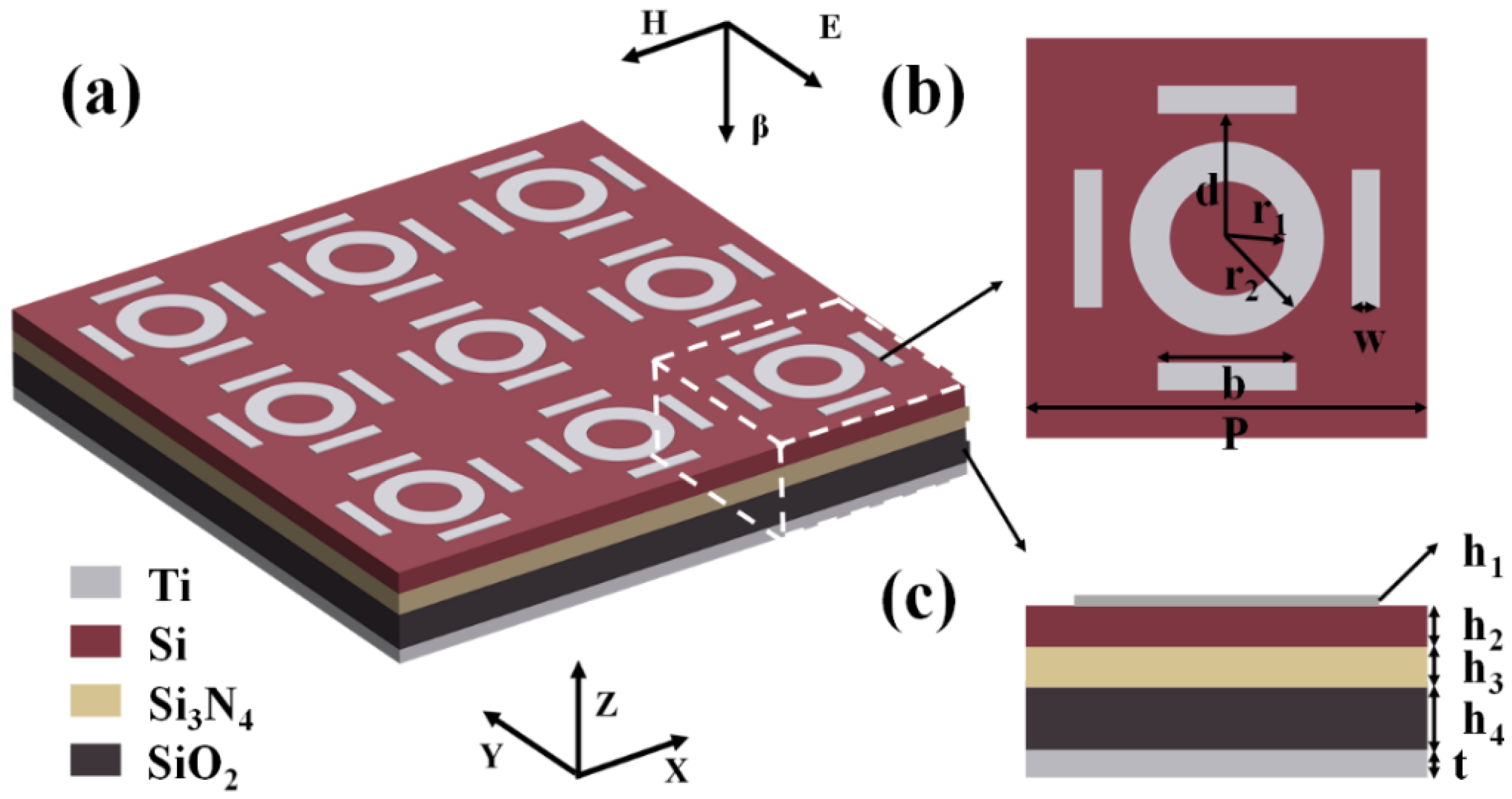
| P | d | b | w | r1 | r2 | h1 | h2 | h3 | h4 | t |
|---|---|---|---|---|---|---|---|---|---|---|
| 2.9 | 0.9 | 1 | 0.2 | 0.4 | 0.7 | 0.02 | 0.3 | 0.3 | 0.5 | 0.2 |
| References | Band Range with Absorption over 90% | Mean Absorption in the Band Range | Structural Layers |
|---|---|---|---|
| [69] | 5 μm (8–13 μm) | 96.7% | Ti-SiO2-Ti |
| [70] | 7.23 μm (8.98–16.21 μm) | 94.1% | Cr-Ge-Si3N4-Ti |
| [71] | 0.71 μm (354–1066 nm) | 97% | Ti-SiO2-Al |
| [72] | 6 μm (8–14 μm) | 94.50% | Ti-Ge-Ti |
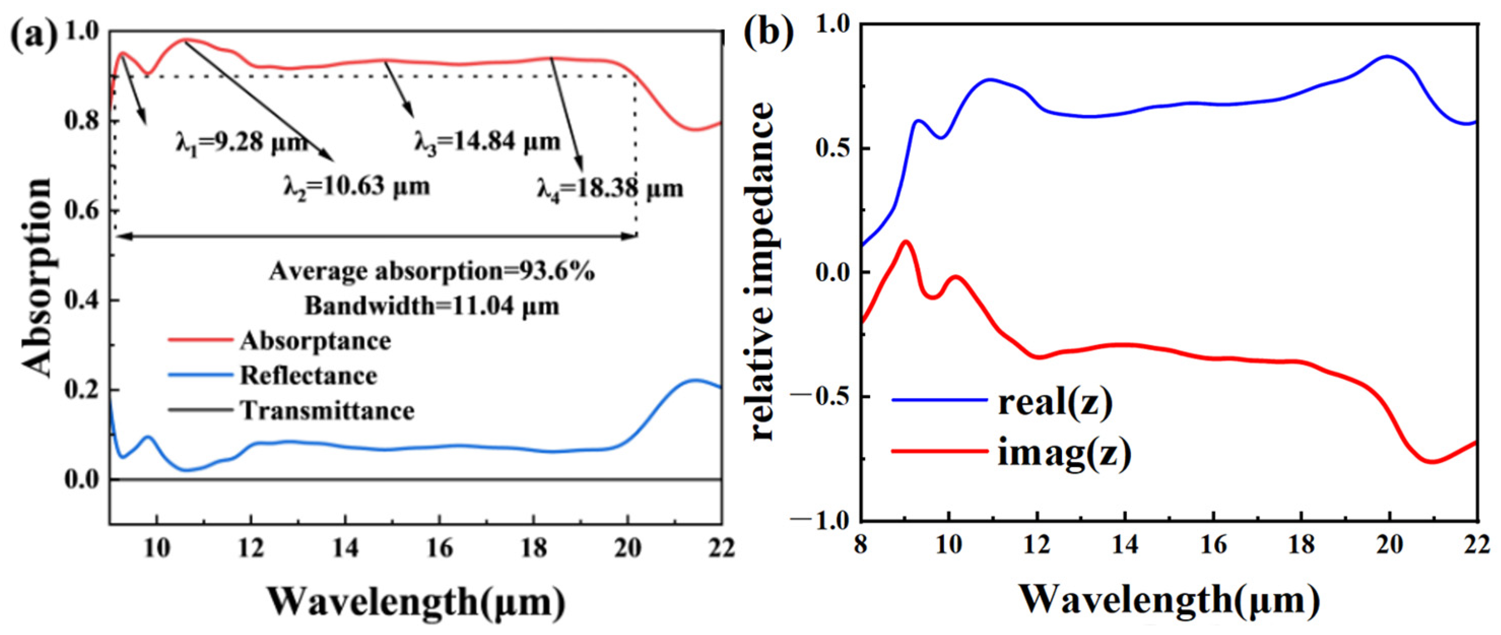
| Proposed absorber | 11.04 μm (9.10–20.14 μm) | 93.6% | Ti-Si-Si3N4-SiO2-Ti |
Disclaimer/Publisher’s Note: The statements, opinions and data contained in all publications are solely those of the individual author(s) and contributor(s) and not of MDPI and/or the editor(s). MDPI and/or the editor(s) disclaim responsibility for any injury to people or property resulting from any ideas, methods, instructions or products referred to in the content. |
© 2025 by the authors. Licensee MDPI, Basel, Switzerland. This article is an open access article distributed under the terms and conditions of the Creative Commons Attribution (CC BY) license (https://creativecommons.org/licenses/by/4.0/).
Share and Cite
Wang, J.; Yang, H.; Yi, Z.; Wang, J.; Cheng, S.; Li, B.; Wu, P. High Absorption Broadband Ultra-Long Infrared Absorption Device Based on Nanoring–Nanowire Metasurface Structure. Photonics 2025, 12, 451. https://doi.org/10.3390/photonics12050451
Wang J, Yang H, Yi Z, Wang J, Cheng S, Li B, Wu P. High Absorption Broadband Ultra-Long Infrared Absorption Device Based on Nanoring–Nanowire Metasurface Structure. Photonics. 2025; 12(5):451. https://doi.org/10.3390/photonics12050451
Chicago/Turabian StyleWang, Jiao, Hua Yang, Zao Yi, Junqiao Wang, Shubo Cheng, Boxun Li, and Pinghui Wu. 2025. "High Absorption Broadband Ultra-Long Infrared Absorption Device Based on Nanoring–Nanowire Metasurface Structure" Photonics 12, no. 5: 451. https://doi.org/10.3390/photonics12050451
APA StyleWang, J., Yang, H., Yi, Z., Wang, J., Cheng, S., Li, B., & Wu, P. (2025). High Absorption Broadband Ultra-Long Infrared Absorption Device Based on Nanoring–Nanowire Metasurface Structure. Photonics, 12(5), 451. https://doi.org/10.3390/photonics12050451