1. Introduction
Micro scale optical mechanisms play a significant role in the world of optical communication devices. A specific purpose system can be built using the interconnection of designs with distinct properties to recreate a more complex but task-oriented light modulator. Various element combinations can be used for the designs and may include silicone [
1], silicon-nitrite [
2], gallium-nitride [
3], silicone-gallium [
4], and others. The vertical outline may include strip [
5], slot [
6], buried [
7], and other waveguide profiles, which envelope the confined light. The functionality may vary and include laser sources [
8], sensors [
9], amplifiers [
10], fiber-transmitters [
11], reflectors [
12], and others. These silicon-on-insulator (SOI)-based optical building blocks may be part of the transmission systems in various common near-infrared (NIR) spectra such as C-band [
13] or O-band [
14]. The latter wavelength range is operatable within data centers for communication purposes [
15,
16].
Multimode-interference (MMI) devices share their name with the phenomena in which the self-imaging and Talbot effects take place to multiply the entering optical signal outline periodically in the direction of propagation of light [
17]. An MMI-based primary operation section has been shown to be suitable for wavelength-division-de/multiplexers (WDMs) [
18], power splitters/combiners [
19], polarization splitters/combiners [
20], signal processors (logical gates) [
21], and others. In those devices, transverse electric (TE) or transverse magnetic (TM) polarization may be used. This type of technology is compatible with complementary metal-oxide semiconductor (CMOS) processes with the advantages of a small footprint, low mass manufacturing cost, and high tolerance to fabrication deviations, while maintaining low losses in NIR wavelengths [
22,
23].
An angled-MMI (AMMI) coupler features single-mode access waveguides and a multimode body, with the input/output waveguides tilted relative to the MMI body and the main propagation direction. This design minimizes reflections that would otherwise return to the laser source, offering an advantage over conventional MMIs and arrayed waveguide gratings (AWGs) [
14].
Although the change in the light path angle affects the light path distance, the self-imaging and Talbot effects will result in a repetitive input field of light along the
z-axis. The propagation direction is along the
z-axis, as shown in
Figure 1. Several papers were published on the possible uses of this outstanding AMMI feature [
14,
24,
25] while stating that additional research can take place.
The optical signal splitter is one of the fundamental mechanisms in opto-electronic systems and a common device in buried dielectric optical waveguide systems. This design allows a single device to serve several end users and enables the distribution of power across multiple outputs, potentially reducing the number of devices needed in a nano-optical system while maintaining similar transmission levels [
26]. In some cases, to achieve the splitting modification early, the splitter is ordered first compared to other sub-system waveguides in the configuration right after the transmitting laser source [
27]. Its location along the propagation direction impacts overall effectiveness significantly; thus, it is important to make device performance robust. The suggested device integrates low power losses, a compact footprint, and tilted single-mode access waveguides to minimize back reflections. This design supports laser stability, ensuring consistent operation and reliable optical data transmission in O-Band systems [
28].
SOI nano waveguides and passive dielectric modulators use diverse device geometries and various material combinations to obtain an advantage in shorter beat length with reduced propagation length [
29], a decreased optical loss [
30], a difference in the refractive index [
31], reduced back reflections to the laser source [
24], doping complexity [
32] and others.
The glass type insulator silica is considered low absorbent [
33], and silicon nitride (SiN) shows flexible properties such as a lower thermo-optic coefficient, greater fabrication tolerance [
34], and low back reflections [
35], and is, therefore, a candidate for passive light transmission. Both materials are widely used for passive and active silicon photonic devices and high-density integration. Silica and SiN film fabrication is CMOS compatible with manufacturing methods like thermal oxidation and low-pressure/plasma-enhanced chemical vapor deposition (LPCVD/PECVD, respectively) equipment, which enables cost-effective volume production [
36].
In this paper, we introduce the design and simulated analysis of a two-channel AMMI-based passive waveguide with a SiN buried core and silica cladding. The device functions as a 1 × 2 signal splitter with an operating wavelength of 1.31 µm. The design was carried out using RSoft-CAD. Simulations, optimizations, and analysis for loss, imbalance, back reflections, bandwidth, tolerances to manufacturing errors, and other parameters were conducted using software solvers, and theyrelied on the full vectorial beam propagation method (FV-BPM), finite-difference time domain (FDTD), and others, alongside MATLAB version R2022b scripts.
2. Buried Waveguide AMMI Splitter Structure and Theoretical Aspect
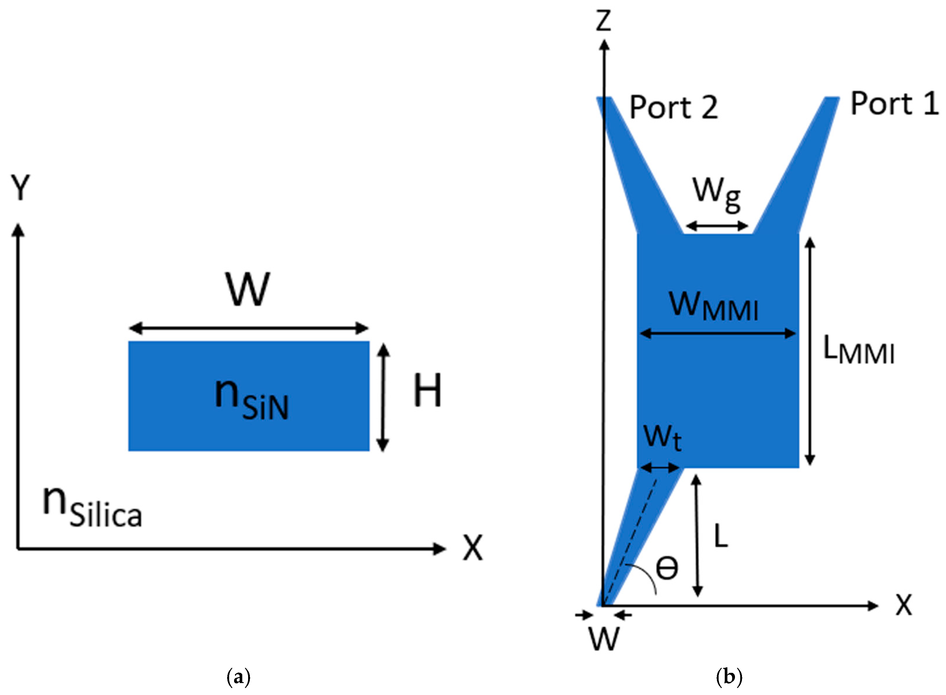
A single-mode tapered input waveguide was used to enable coupling between the Gaussian monochromatic quasi-TE polarized laser source signal and the MMI structure to allow optical power transfer. A multilayered thickness layout was established to create the silicon nitride core in blue color and the silica mid-upper and lower cladding areas in white color, as can be seen in
Figure 1a, which shows the
x-
y plane schematic sketch of the device by their chemical formulae SiN and silica, respectively. The thickness value, which is kept constant throughout the length of the device, is denoted by a value of H. The thickness and width are denoted by Y and X axis, respectively.
Figure 1b depicts the schematic sketch on the
x-
z plane of the overall 1 × 2 power splitter AMMI device, including the input tapered access waveguides with a transitional width. The overall width of the MMI bulk core is set to W
MMI, the gap between the ports is measured as W
g, and the length of the access waveguides in the
z-axis is marked by L. The length of the MMI section was denoted as L
MMI, and the output ports were appointed as Port 1 (Right) and Port 2 (Left). The tilt angle denotes the desired misalignment of the access taper. Therefore, the optical path direction was set to θ. The direction of propagation and the changing width of the design are denoted by the Z and X axes, respectively.
For the chosen simulation, the wavelength of 1.31 µm was analyzed. For this NIR wavelength in the O-Band communication spectral range, the refractive indices of SiN and silica were set by RSoft-CAD to the values of 1.994 and 1.447, respectively. Although the width of the MMI core does not undergo changes in the direction of propagation, for the single-mode access waveguide, a tapered structure is introduced in which width changes from narrow width (W) to broad width (Wt) for the input and by a similar matter is inverted for the output.
The tapered input and output access waveguides function as source-MMI and MMI-forward couplers, enabling mode spot size conversion. In addition, the port’s tilt angle is aligned or mirrored to the input optical path. This is crucial to maintain adequate optical field progression in the adjusted optical path.
Firstly, an estimation of the beat length
Lπ was performed according to Equation (1), where
neff is the effective refractive index of the SiN core film for the fundamental mode,
Weff is the effective width of the MMI coupler, and
λ stands for the monochromatic operational wavelength [
24].
Equation (2) calculates the length of the MMI bulk
LMMI, where
p is a reoccurrence multiplier of the field profile,
Lπ is the beat length, and
N denotes the number of outputs of the coupler. Equation (2) will estimate the regions that satisfy the self-imaging effect in consideration of the total internal reflection effect [
14] to achieve the desired optical field at the output with the shortest possible overall device length [
37].
Equation (3) denotes the effective width of the MMI bulk
Weff. The effective width considers the lateral penetration depth of the mode field at the core film boundaries and is known by the Imbert–Fedorov effect. For TE polarization,
Weff is given by the following equation, where
nclad is the effective refractive index of the cladding material [
37].
To analyze the transmission and the effect of the device on the suggested input signal, several parameters were calculated. The excess loss will show the simulated total power loss of the device and is shown in Equation (4), where
Pin is the input power and
Pout is the combined output power from both output ports.
The imbalance is shown in Equation (5) and depicts the calculation of the nonuniform power distribution at the output ports, where
P1 and
P2 depict the output power from output port 1 and port 2, respectively.
To determine the operational range of the device, several critical constants were strain-tested, and the results are shown as tolerability for deviations in value for those parameters. Tolerance levels will depict the loss as a function of thickness, width, length, and tilt angle, in addition to the spectral response all this while considering manufacturing ability and resolution.
3. Simulation Results
To perform the simulations for our suggested 1 × 2 AMMI splitter design, RSoft Photonics CAD suite software was used with BEAMProp solver, which utilizes FV-BPM to numerically approximate the solution to the wave equation and the field energy in the direction of propagation assuming the mode is hybrid thus taking into consideration both major and minor field components. Using this advanced solver, we were able to precisely design, model, and simulate light propagation for the input monochromatic wavelength to numerically solve the wave equations and evaluate device performance in terms of mode solution, optical progression, and power distribution. In addition, we were able to define the geometrical parameters of the device along with the definition of materials, all of which allow precise simulations and results. The MOST application was used to optimize the device, and graphs were processed using MATLAB scripts based on RSoft-generated output.
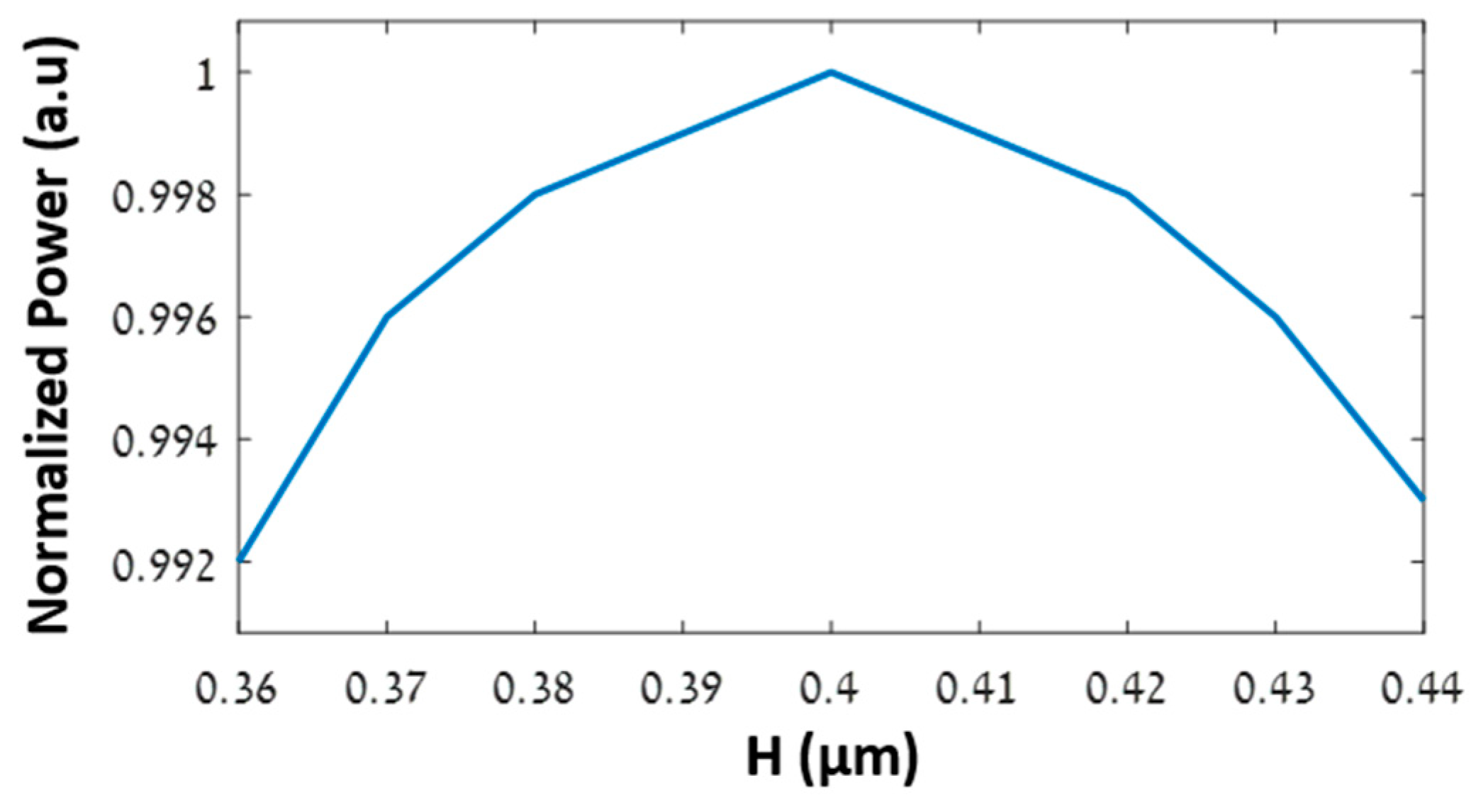
A single-mode SiN core waveguide was tested to determine the best possible fit of the device height in the
y-axis dimension to allow proper mode propagation, which will be used in further tests. As stated, the thickness value is denoted by H, and it was set to 0.4 µm, as seen in
Figure 2 in terms of normalized power, considering that the input power is 1. This ensures that a propagating fundamental mode can be sustained in the waveguide core. A large deviation from the suggested thickness values may introduce various challenges such as increased propagation loss, mode distortion, mode coupling mismatch, or larger device dimensions [
38].
A relatively wide range of thickness values was tested to review the overall impact of deviations from the selected thickness. Simulation results show almost lossless power transmittance at the selected value. Over the whole tested range, which covers possible manufacturing imperfections of thicknesses of up to ±0.04 µm (±40 nm), a small loss of 0.035 dB is shown in the edges of the range, with even smaller losses for more minor thickness variations. Modern CVD-based manufacturing machines and methodologies are shown to have sufficient precision for the suggested thickness range to reliably deposit the requested layer [
39].
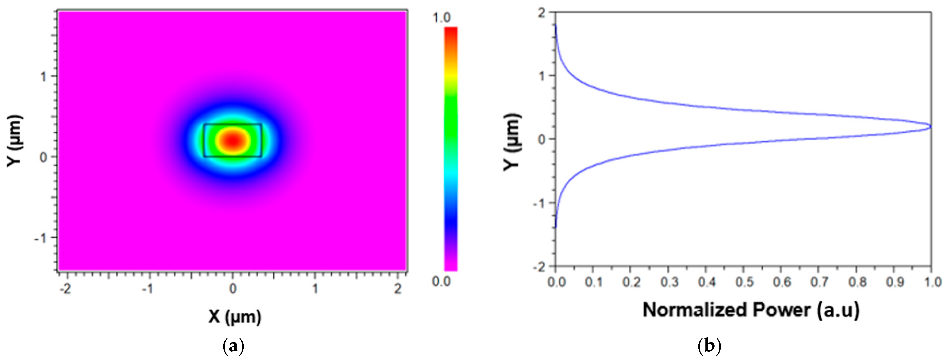
In addition, we simulated the non-tilted and non-tapered single-mode access waveguide to resolve the single-mode solution for the quasi-TE polarization. The mode profile, including lateral dimensions, core field distribution, and evanescent field profile, alongside the transverse refractive index profile, were analyzed. The source was set at a monochromatic wavelength of 1.31 µm with a Gaussian shaped profile for this and all other simulations unless stated otherwise. The horizontal dimension, also noted as device width W, was chosen to satisfy great optical power containment in the core section and was set to 0.7 µm, as can be seen in
Figure 3a. As intended and expected, the mode can be sustained along the core of the suggested design. Simulation results also include the calculated approximation of 1.64 for the effective refractive index, n
eff.
Figure 3b shows the power distribution of the inserted mode in
y-axis.
During light propagation through the tapered access waveguides, spot size transformation occurs due to the varying width. At the taper-MMI coupling cross-section, the width was set to 1.1 µm, while the taper length along the z-axis was 21.45 µm.
It can be seen from
Figure 3b that the mode power concentration is at the height of 0.2 µm, which aligns with the physical core center in terms of
y-axis vertical value.
Calculations were performed based on Equations (1)–(3) to determine the theoretical values of the optical path length in the
z-axis for the desired interference and subsequently the MMI bulk length, assuming purposed width (W
MMI) of 4.5 µm. Using Equation (3), the effective width was estimated as 5.04 µm. The selected core dimensions ensure the fundamental TE mode solution for the SiN buried waveguide, resulting in strong light confinement, as illustrated in
Figure 3b. A device with slightly different values may be operable, provided that other adjustments are made. Significantly decreased dimensions may cause excessive modal leakage and increased radiation loss. Conversely, increased dimensions may introduce multi-modal behavior or unwanted mode conversion and interference. To determine the MMI section length, we used Equation (2) by filling in
p = 1 for the first repetitive cycle as the shortest length is desired and beat length as 42.3 µm based on Equation (1), which resulted in an estimated value of 63.45 µm assuming
N = 2. These values were used as the initial conditions for some of the final dimensions of the device.
In general, splitters with some level of asymmetry face an additional aspect of a tradeoff as the interference is slightly favorited to either of the ports based on the geometrical features of the design, which may cause some shifts in power imbalances between the outputs. For
Figure 4,
Figure 5 and
Figure 6, tolerance variations are tested only for the parameter of interest while other values are kept constant.
Figure 4a depicts the simulation results for output power in terms of excess loss and imbalance, both in dB, for the MMI length L
MMI.The excess loss is colored orange and denoted by empty squares, while the imbalance is colored blue and marked with empty circles; both are shown on the right and left y-axis, respectively.
To determine the performance of the device for possible manufacturer imprecision, a range of ±2 µm was tested in terms of transmittance. It has been concluded that the maximum excess loss and imbalance for this range are at most 1.4 dB and 0.1 dB, respectively. The preferred value of MMI bulk length was chosen as 58.5 µm to achieve the lowest possible losses in both parameters, which is in good agreement with the calculations and the theoretical assumptions.
Similarly, MMI SiN bulk width was tested while maintaining L
MMI at 58.5 µm, as can be seen in
Figure 4b. The selected value for W
MMI was set to 4.5 µm to achieve the lowest excess losses combined with reduced imbalance, which were measured as 0.21 dB and <0.01 dB, accordingly. For the tested W
MMI range of ±0.2 µm, relatively high excess losses of over 4 dB and an imbalance of slightly over 0.1 dB are expected.
To determine the optimal tilt angle for the input and output access waveguides, a range of angle values was simulated to achieve a balance between minimizing back reflections and reducing optical losses. This approach transforms the device into an effective AMMI. In addition, tilt angle directly impacts the optical path length of the input light signal and, therefore, affects device dimensions, primarily on the
z-axis.
Figure 5 depicts the suggested device excess loss and imbalance at the output ports as a function of the tilt angle θ.
The performance of the device was evaluated for a tilt angle range of ±2° degrees to understand the impact of deviations on the transmission, as setting the light path angle to a non-zero value impacts the interference pattern. The selected value for θ was set to 5°degrees, in which the excess loss is 0.21 dB and the imbalance is <0.01 dB. While the chosen tilt angle does not yield the lowest excess loss, it was selected based on a tradeoff between MMI length and width, which are correlated with θ by a shift in the light path and by the changed coupling conditions, respectively. A smaller tilt angle slightly reduces excess loss but increases the device length and may lead to higher back reflections, as shown in
Figure 5b. This AMMI splitter is designed to ensure stable and predictable power distribution, making imbalance a key metric. Excess loss is important, but maintaining equal power distribution is critical for reliable operation in optical networks, and a tradeoff must be considered. The selected θ value accomplishes our intention for this design by balancing excess loss, power distribution, dimensions, and back reflections. The limitation of back reflection is a critical parameter as it can significantly degrade the signal quality, and it is highly dependent on the laser source.
Currently, a commercial laser typically can tolerate a back reflection in the range of −35 to −38 dB. This limitation was considered for designing light modulators [
40,
41,
42]. Back reflection measurement was a decisive factor in the operatable properties of the designs. To mitigate this, we selected a 5-degree angle as it provides a lower back-reflection compared to other angles, effectively minimizing signal degradation and ensuring better performance.
The sensitivity of the device to losses increases proportionally with the tilt angle, but the overall sensitivity of excess losses and imbalance remains moderate in the tested range. A lower tilt angle can somewhat reduce losses but may compromise the goal of minimizing back reflection. It could also increase the overall device footprint, particularly in designs with multiple cascaded splitters or other multi-device coupling configurations. As stated, changes in θ allow flexibility in the z-axis dimensions.
Figure 6a shows the final interference pattern of the transmitted optical signal throughout the device alongside the colored power scale, assuming input power is normalized to 1. The solved quasi-TE mode was applied in the launch settings of the final device geometry. The adiabatically tapered input and output waveguides, which act as mode spot size converters, are tilted and coupled to the MMI section to form the AMMI 1 × 2 power splitter.
A successful power splitting was achieved for the investigated wavelength, with an excess loss of 0.22 dB and a simulated imbalance of <0.01 dB. The footprint of the suggested device is 101 µm × 7.8 µm, while the gap between the ports Wg resulted in 3.57 µm. Given the optimized conditions of simulations, the reported values for both imbalance and excess loss represent theoretical upper bounds rather than expected fabrication outcomes. Hence, it is impractical to state an imbalance as low as 0.001 dB. We indicate a more practical imbalance range of <0.01 dB.
Figure 6b illustrates excess loss and imbalance as functions of wavelength across the O-band, providing insight into the device’s operational ability to alter the wavelength of the source. The selected wavelength of 1.31 µm achieves the optimal transmittance, as expected due to the careful optimization.
The device functions as an operational passive coupler even at the edges of the O-band range, with a maximum excess loss of 1.57 dB and a maximum imbalance of 0.05 dB.
The diverted optical path is caused by tilting the access waveguide in the interconnection between the input source and the overall device. This was performed to achieve the desired range of low back reflection values, which helps reduce optical power returning to the source. Lower back reflection ensures that the passive optical coupler does not interfere with the source, allowing it to function reliably within the telecommunication system. As expected, our splitter was optimally designed to function in TE mode, which is why it performs best in this mode. The proposed design is better suited for TE mode due to its optimized characteristics. However, the proposed splitter can also operate in TM mode, as shown in
Figure 7a. This figure illustrates the light intensity propagation of a 1310 nm wavelength from the input angled section into the MMI coupler and through to the two output ports. The excess loss of the splitter in TM mode is 0.73 dB, with an imbalance of 0.22 dB, as extracted from
Figure 7b.
Figure 8a depicts the FDTD simulation in the spatial contour resulting from the FullWAVE solver. An additional waveguide segment (orange color) was added before the elongated input access waveguide with similar dimensions, and a backward signal monitor (green color) was added to sense any light that otherwise would have returned to a sensitive source.
Simulation results demonstrate the ability of the proposed device to achieve consistently low back reflection, with a measured value of −40.96 dB at the operational wavelength and values of up to −39.67 dB over the O-band spectrum, as illustrated in
Figure 8b, aligning well with theoretical expectations for AMMI devices with SiN core. These findings highlight the device potential for data center applications that demand stable, reliable, and consistent signal distribution.
Table 1 summarizes an extensive literature review to compare various previously studied AMMI splitters with two output ports. The parameters that were reviewed include MMI width and length, operational wavelength spectrum, imbalance losses, excess losses, back reflection, and year of publication. In addition, different materials, cascading configurations, and core geometries were used, as stated under the Power Splitter Type column.
The literature review presented in
Table 1 highlights the advanced performance and unique attributes of our proposed 1 × 2 SiN AMMI power splitter in relation to existing devices. Notably, our device demonstrates an excess loss of just 0.22 dB and an exceptionally low imbalance of <0.01 dB, surpassing comparable devices. Additionally, it exhibits excellent back reflection, recorded at −40.96 dB, which indicates very good source immunity and signal integrity at the operational wavelength. The relatively compact design dimensions are in the range of other reviewed devices and are suitable for applications with high efficiency and space optimization needs. In addition, for O-band optical communication, the splitter’s compact footprint is crucial, particularly in densely integrated transceiver systems where space is at a premium. This comparison highlights our device’s potential as an effective, high-performance component for high-speed, reliable data transmission in compact and space-constrained environments.
4. Conclusions
This paper introduced additional research for the innovative geometric change in the passive AMMI couplers family, which is the inclination of the single-mode access waveguide and the redirection of the input light signal in an angle compared to the interference medium. The researched design was based on a silicon nitride core with a thickness of 0.4 µm and silica cladding. It was set up to be tilted at a 5° degree angle to the direction of propagation, with an MMI section length and width of 58.5 µm and 4.5 µm, respectively. The total device footprint layout resulted in 101 µm × 7.8 µm for length × width, respectively, while targeting the central wavelength of the O-band range of 1.31 µm. The distance between the output ports Wg resulted in 3.57 µm.
A successful transmission of an optical field from the input source to the output ports was achieved with an excess loss of 0.22 dB and an inconsequential imbalance of <0.01 dB. For the tested O-band spectrum, a decent transmittance showed an excess loss of 1.57 dB and an imbalance of 0.05 dB.
In terms of back reflections, a significantly low value of −40.96 dB was achieved. In addition, it was concluded that while, in general, a deviation in the value of critical parameters may cause decreased performance, the MMI bulk width is relatively impactful on excess loss compared to other parameters in the tested scope.
The spatial parameters, mode conversion efficiency, interference characteristics, and reduced back reflections align well with theoretical predictions and perform competitively with similar devices.
Beyond optical communications in the O-band, this splitter is well-suited for integration into data center networks and offers compact design, high signal integrity, and multi-channel handling with minimal interference. Its low excess loss and back reflection suppression make it ideal for high-speed, reliable data transmission in dense computing environments.
The suggested device can be further refined in manufactory with current technologies and can attain the fine resolution required for the selected parameter value ranges. While the simulated results show a better edge in performance, it is expected that a physical SOI-based device production will encounter additional practical losses.
For further work, we would suggest further research on the underrated angled-MMI passive coupler device family for various purposes and goals, which can be undertaken by modifying the wavelength, materials, geometry, dimensions, and angles used while maintaining the notion of inclined input and output ports to maintain the benefit of the greatly reduced back-reflections and device footprint. In addition, the losses stated above are also open to further experimentation and may include scattering, coupling, and alignment losses.


