1. Introduction
Rapid industrialization has intensified water pollution, with heavy metal contamination posing critical risks to human health and ecosystems [
1,
2,
3]. Nickel, a prevalent pollutant, is hazardous at concentrations exceeding 0.02 mg/L, as outlined by the World Health Organization (WHO). Conventional methods for nickel detection, such as atomic absorption spectrometry (AAS) and inductively coupled plasma-mass spectrometry (ICP-MS), suffer from high costs, lengthy procedures, and secondary pollution risks [
4,
5,
6].
The emergence of terahertz wave detection technology offers a novel approach to address these challenges. This technology combines the unique electronic characteristics of Weyl semimetals with the high penetrability of terahertz waves, enabling the rapid and accurate measurement of nickel concentrations in water [
7,
8,
9,
10]. In comparison with traditional detection methods, terahertz wave technology not only improves detection efficiency but also cuts down costs, thus presenting promising application prospects.
Weyl semimetals exhibit exceptional optoelectronic properties due to their non-trivial topological invariants and linear dispersion near Weyl points [
11,
12,
13]. Their distinctive topological features and surface states pave the way for the development of terahertz chip technology. The existence of band-crossing points with linear dispersion relations, known as “Weyl points”, accounts for their outstanding electron mobility and low carrier recombination rates in the terahertz spectrum [
14,
15,
16].
Recent research suggests that the electron mobility of Weyl semimetal materials can reach 10
5 cm
2/V·s at room temperature, far exceeding that of conventional semiconductor materials. When these materials are used as active layers in terahertz chips, this high mobility enables rapid response and high-sensitivity detection [
17,
18].
The terahertz frequency range is generally defined as the frequency spanning from 0.1 to 1 THz. In this frequency band, photon energy is relatively low, which enables real-time monitoring without causing ionization or chemical changes in the samples. This feature endows non-contact detection with distinct advantages, facilitating non-destructive analysis of the samples.
Moreover, many substances display unique fingerprint spectral features within the terahertz range or exhibit different responses to terahertz waves of the same frequency, which can be ascribed to their carrier properties or to other physical characteristics. Therefore, the utilization of terahertz waves for the detection of these substances can achieve a high degree of accuracy. By taking advantage of these specific response mechanisms, rapid and precise sample detection can be achieved [
19,
20].
This research study presents a terahertz-responsive chip. It utilizes Weyl semimetal thin films as the active layer, which is complemented with sub-wavelength metallic structures acting as the chip substrate to augment the response to terahertz waves. The experimental method entails depositing a liquid containing nickel metal particles onto the chip and then irradiating it with continuous terahertz waves for testing purposes. Through an exploration of the chip’s responses to terahertz waves when exposed to liquids of different concentrations, a relationship between the concentration and the terahertz response can be established. This, in turn, enables a rapid and non-contact approach for detecting the concentration of nickel metal particles.
2. Materials and Methods
Terahertz chip technology is a novel development in sensing methods, which is based on the fundamental physical properties of terahertz waves. These waves are located in the spectral range between microwaves and infrared radiation, possessing unique penetrative and spectral properties that provide significant advantages in substance detection applications.
When it comes to evaluating the nickel concentration in aqueous solutions, the terahertz chip emits terahertz waves and then analyzes the signals generated from the interaction between these waves and the water sample. Specifically, when terahertz waves pass through a water sample containing nickel particles, the absorption and scattering phenomena caused by these particles have an impact on the terahertz waves, resulting in changes in the photocurrent produced by the chip. This alteration in photocurrent can be accurately measured using a digital source-meter.
A quantitative model that correlates the nickel concentration with the photocurrent after the incidence of terahertz waves is established. This enables the rapid and accurate determination of nickel levels in water. This technology not only improves the detection sensitivity and selectivity but also shows great potential for environmental monitoring applications.
Compared with terahertz time-domain spectroscopy, this approach features a simpler device configuration and better operational feasibility. Device stability was ensured through the following measures. Firstly, magnetron sputtering under optimized conditions ensured uniform thin-film deposition. Secondly, a 30 s SiO2 coating isolated the active layer from oxidation and humidity.
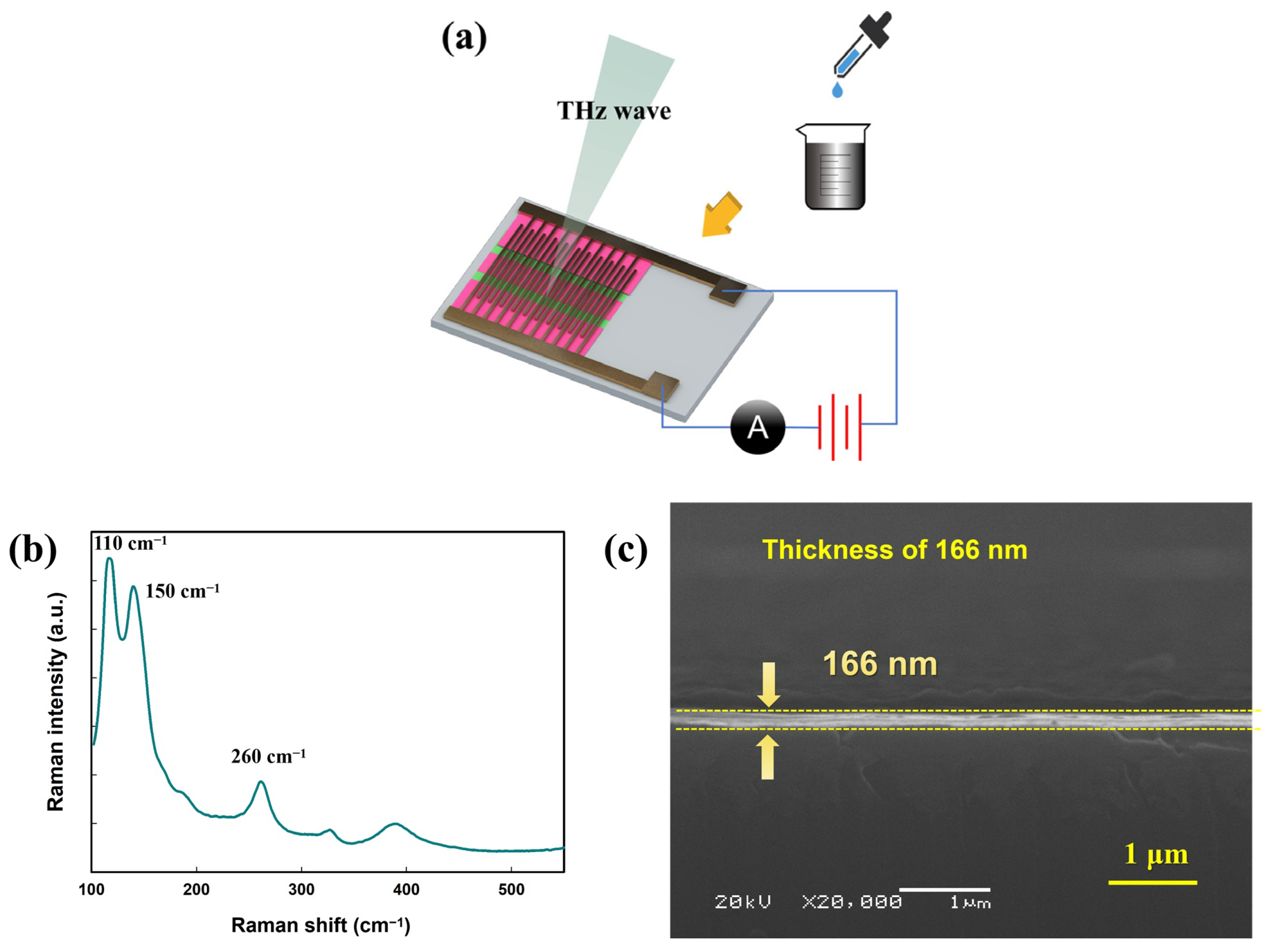
To evaluate water samples with varying concentrations of nickel particles, a sensing chip based on Weyl semimetals was first designed to enhance sensitivity during the interaction between terahertz waves and the samples. Subsequently, a micro-current probe platform was constructed. The terminals of the probe were connected to a digital source-meter, which served as both a power supply and an ammeter. The samples were irradiated with terahertz waves, and the resulting light currents and dark currents (i.e., the currents measured with and without terahertz exposure, respectively) were recorded. Then, the responses of terahertz waves to different nickel concentrations were calculated. Ultimately, the relationship between the responsivity and the concentration was established to determine the detection limit of the proposed scheme. A schematic diagram of the experimental setup is shown in
Figure 1a.
Firstly, a sensing chip based on Weyl semimetals was fabricated. The process was carried out as follows: an active layer made of Weyl semimetal was deposited on the interdigital electrode sensor located on a ceramic substrate. The interdigital electrode of the ceramic substrate was fabricated via the vacuum evaporation technique, in which a copper interdigital structure was evaporated onto the substrate.
The copper interdigital structure had a width of 50 μm and the electrodes were separated by 50 μm. The Weyl semimetal WTe2 was chosen as the active material for the chip. The WTe2 thin film was synthesized via the magnetron sputtering method, and the detailed procedure was as follows: First, the air pressure inside the chamber was decreased to 8 × 10⁻⁴ Pa, after which argon gas was introduced. Then, the WTe2 target was coated in radio-frequency mode. During this process, the argon gas flow rate was kept at 50 standard cubic centimeters per minute (SCCM), the power was set at 50 W, and the deposition time was 220 s. Subsequently, silicon dioxide (SiO2) was deposited on the device for 30 s. This was carried out to isolate the active layer from the atmosphere and improve its stability.
After the thin-film preparation was completed, a Raman spectroscopy analysis was carried out, the results for which are shown in
Figure 1b. The Raman spectrum displayed distinct characteristic peaks at around 110 cm
−1, 150 cm
−1, and 260 cm
−1, which are consistent with previously reported results in the literature. Moreover, the relatively narrow Raman spectrum indicates that the thin film has excellent crystallinity, which is beneficial for promoting higher carrier mobility and improving the high-speed detection performance of the device.
To determine the thickness of the thin film, a 1-mm-thick silicon wafer was used during the magnetron sputtering process. After the thin-film deposition was completed, the silicon wafer was sectioned, and the thickness of the deposited thin film was measured via high-precision scanning electron microscopy (SEM). The measurement results are shown in
Figure 1c. The data suggest that the thin film has excellent overall flatness, indicating a high-quality deposition of the WTe
2 material on the substrate. The measured thickness of the thin film is 166 nm. Maintaining an optimal thin-film thickness is crucial because excessive thickness can hinder carrier migration. Specifically, when carriers migrate within the surface layer, the migration rate increases, leading to improved device response times. In contrast, if the thin film is too thick, carrier migration may occur not only on the surface but also in the z-direction, which can reduce the migration rate and, as a result, slow down the overall response rate of the device.
The micro-current testing system designed to evaluate the terahertz response of nickel solutions comprises three primary components: a tungsten-steel probe platform for assessing chip micro-currents, a continuous terahertz source that generates the response, and a digital source-meter that supplies direct current (DC) power and measures current data. To mitigate electrostatic accumulation, a probe tip with a diameter of 500 μm was selected for the tungsten-steel probe as the detection device. The continuous terahertz source utilized is a terahertz avalanche diode operating at a frequency of 0.1 THz, with a maximum output power of 70 mW. The output interface of the terahertz source is configured as a horn with a 10° inclination angle, resulting in a light plane that expands with increasing emission distance. The terahertz source is typically positioned 15 cm from the chip, necessitating an initial measurement of the terahertz light spot area at the chip’s location, which is then compared to the effective area of the chip to ascertain the actual power of the terahertz wave incident upon it.
The terahertz irradiation area is quantified using a terahertz camera. Initially, the camera measures the dimensions of the terahertz light spot at a consistent distance from the light source to the detector. The INO MICROXCAM-384I-THz terahertz camera was employed to determine the light-spot area S. To ensure the accuracy of the experimental data, a terahertz power meter (ELVA-1 DPM R-1612) was utilized in direct contact with the emitting end of the IMPATT diode to measure the total power (W). The relationship between the light-spot area S and the effective detection area of the active layer of the chip s allows for the calculation of the incident power on the terahertz detector as W/S × s.
To characterize the detection capabilities of the device, including I-V curves, response (R
A), noise equivalent power (NEP), and specific detectivity (D*), we employed a light-and-dark current comparison method based on photocurrent excitation. The terahertz detector was centrally positioned on the probe platform, with two tungsten probes contacting the device’s metal electrodes, connected in series with a DC power supply and a picoammeter. A terahertz avalanche diode (TeraSense IMPATT diode @ 0.1 THz) served as the terahertz source, while a digital source-meter (KEITHLEY 2400) recorded the I-V curves. A schematic representation of the experimental setup is provided in
Figure 2. Furthermore, during the experiment, we reversed the polarity of the connections for testing purposes, and the results remained consistent, thereby excluding the influence of the electric field direction.
To further clarify the role of the interdigital electrode configuration in enhancing the terahertz field, we utilized electromagnetic simulation software CST Studio Suite 2023 to analyze the field distribution on the device’s surface after terahertz waves were incident on a metallic sub-wavelength structure.
The existence of fine sub-wavelength features at the metal-dielectric interface may promote the generation of localized surface plasmons (LSP) on these structures. LSP can confine electromagnetic field energy to a tiny scale and mainly occur on small particles with closed surfaces. The frequency of LSP is affected not only by the materials of the metal and dielectric but also by the geometry and dimensions of the microstructures at their interface [
21,
22].
The interdigital spacing was set at 50 μm, and the metal structure also had a dimension of 50 μm. Within the sub-wavelength range, specifically at an incident frequency of 0.1 THz, surface plasmons could be excited. The interaction between incident terahertz photons and carriers in the active layer results in the formation of surface plasmon polaritons on the array’s surface.
The plane perpendicular to the chip is defined as the Z-direction. As shown in
Figure 3a, the resulting photocurrent flows within the XY plane, and the electric field distribution is mainly concentrated around the interdigital electrodes of each metallic structure. Notably, the active-layer region without structural features does not support carrier aggregation.
The simulation results suggest that when a Weyl semimetal thin film is deposited on the metallic structure, the confinement of terahertz waves around the interdigital configuration significantly strengthens the interaction between the terahertz waves and the active layer.
3. Results
Nickel particles act as scattering centers, altering the local dielectric environment. This modifies surface plasmon polaritons (SPPs) at the WTe
2/metal interface, which are highly sensitive to carrier density [
11]. Increased nickel concentration enhances scattering, reducing carrier mobility and increasing photocurrent (as R
A μτ), where μ is mobility and τ is carrier lifetime [
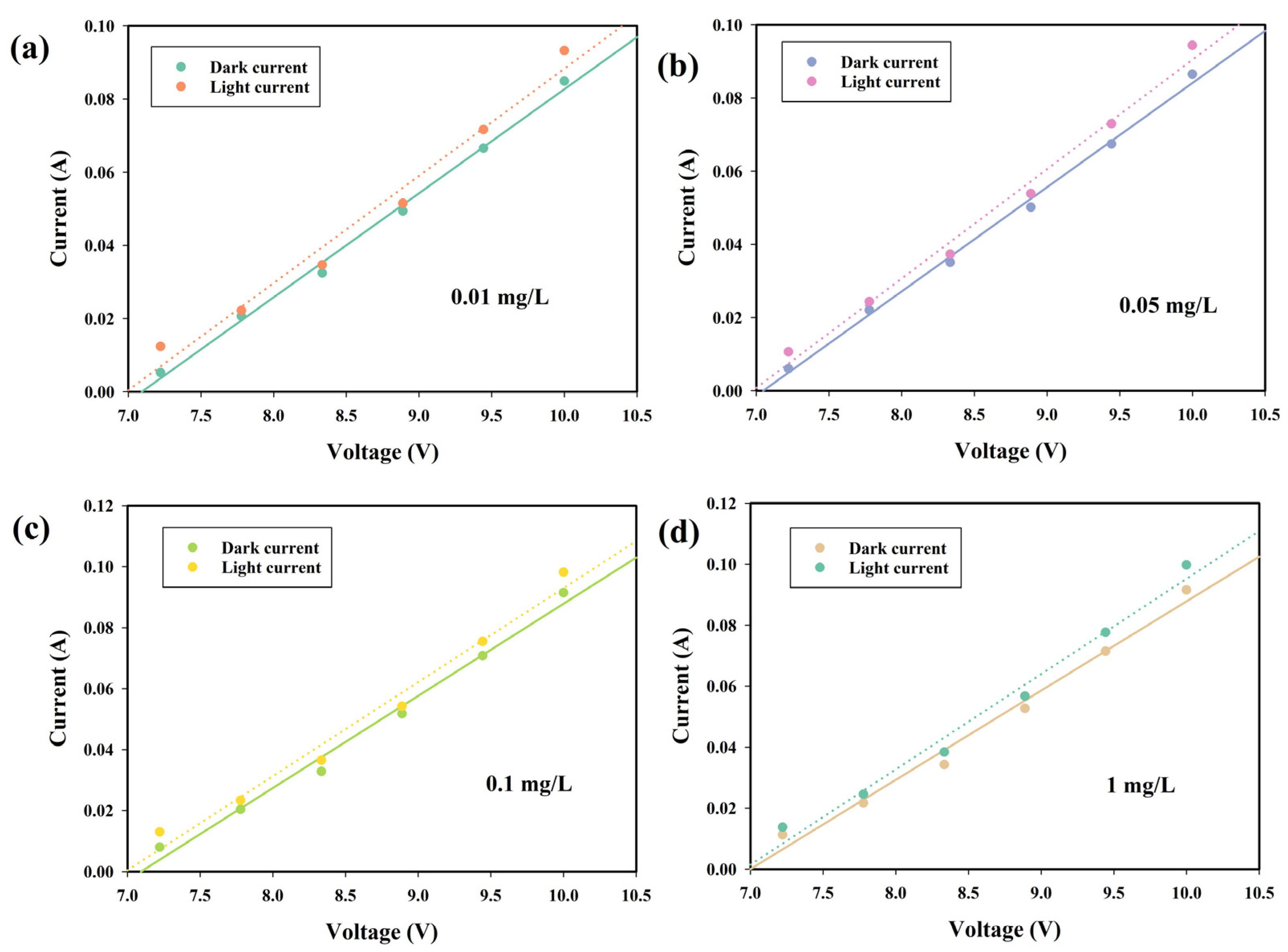
17]. First, we evaluated the light currents and dark currents of the chip by introducing nickel metal particle suspensions with different concentrations. We chose suspensions with four distinct concentration levels of nickel metal particles.
To prepare these suspensions, we used nickel metal particles of different weights and then mixed them with tap water to obtain a homogeneous solution. The resulting mixtures were sonicated for 30 min using an ultrasonic device.
Subsequently, 10 microliters of the suspension were taken with a micropipette and applied to the chip. The dark currents of the solutions at different concentrations were measured without terahertz wave incidence. Subsequently, the photocurrents were recorded under the influence of terahertz radiation at various voltage levels. The experimental results are shown in
Figure 4a–d.
The results indicate that the range of both light and dark currents falls between 0.01 and 0.1 A, suggesting a relatively high current value, which in turn enhances the accuracy of the measurements. Conversely, if the current values are excessively low, the resulting perturbations may obscure the actual terahertz response, making it challenging to discern. Sewage itself exhibits certain frequency-selective absorption characteristics for terahertz waves. The absorption coefficient for terahertz waves with a frequency of 0.1 THz is 220 cm−1. When processing the Nickel Metal Particle data, we subtracted the response of sewage to terahertz waves.
Subsequently, we utilized diverse terahertz detection performance indicators to assess the responsiveness of nickel solutions with different concentrations to terahertz waves. The quality factors of the terahertz detectors were mainly evaluated via parameters such as photoelectric responsivity (RA), equivalent noise power (NEP), and detectivity (D*), which jointly measure the photoelectric conversion efficiency of the detectors.
These quality factors, R
A, NEP, and D*, can be expressed as [
17,
18]:
I is the photocurrent of the device,
P is the incident terahertz power,
S is the effective detection area of the detector, and
Vn is the noise voltage.
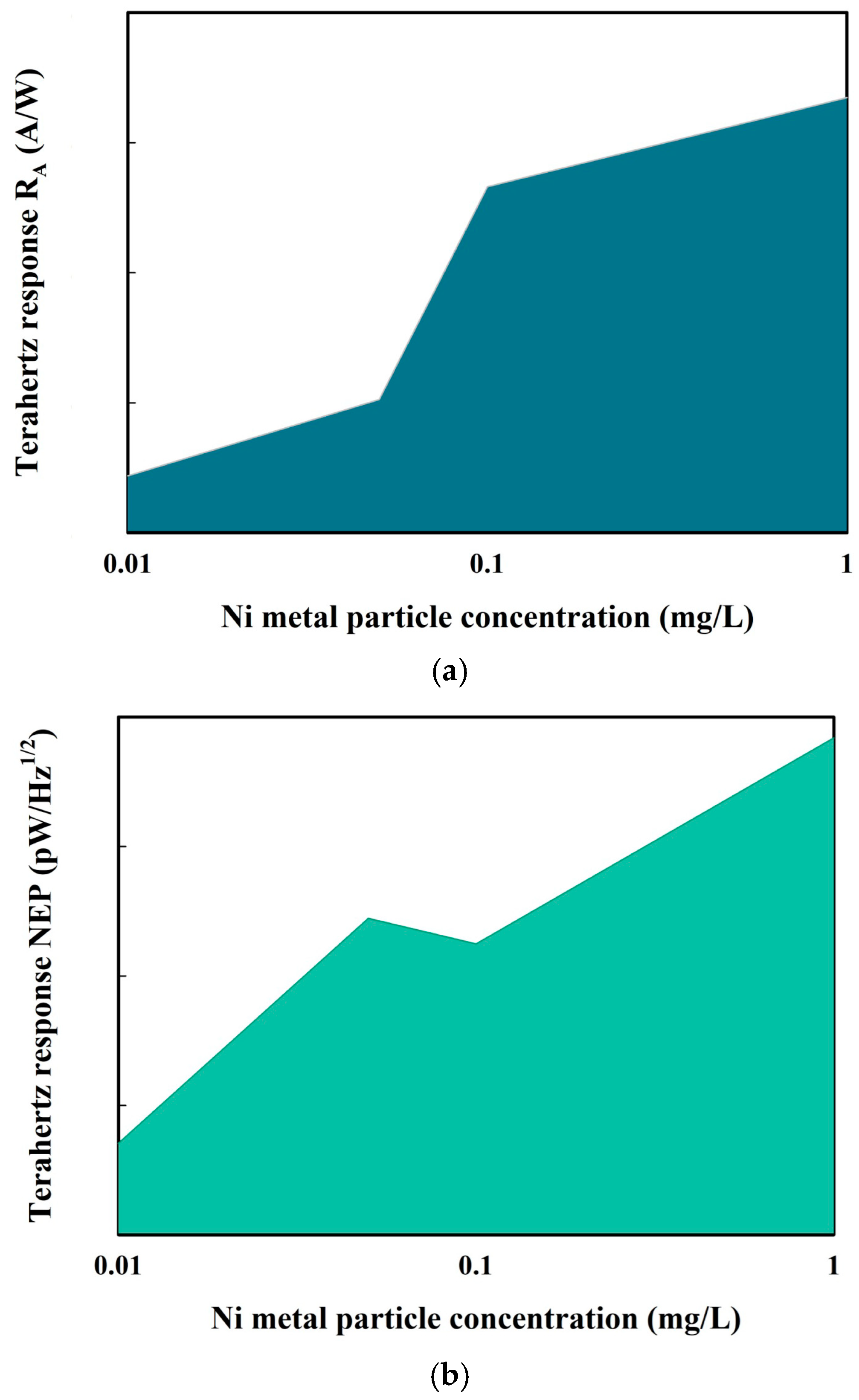
According to the light current and dark current shown in
Figure 4, the data results for three aspects, namely R
A, NEP, and D*, can be obtained, as presented in
Figure 5.
Among these results, at a voltage of 10 V, as the nickel concentration increases—specifically at the four concentrations of 0.01 mg/L, 0.05 mg/L, 0.1 mg/L, and 1 mg/L—the sensitivities are 378, 385, 397, and 412 A/W, respectively, and the equivalent noise powers are 0.54, 0.5, 0.47, and 0.43 pW/Hz, respectively.
The experimental results indicate that there are significant differences in the terahertz responses when doped with nickel-metal particles at different concentrations. As the concentration rises, the high-concentration nickel-metal particles also serve as a medium for carrier migration. However, since the overall concentration remains relatively low, the difference in responsivity changes slightly. As a result, the carrier mobility is enhanced, leading to an increase in responsivity and a decrease in equivalent noise power. Based on these changes, it is feasible to determine the concentrations of metal particles at different levels.
The response time of the device can be determined by referring to the moment when the terahertz source is activated and to the variations in the measured current. Respond time of the device was shown in
Figure 6. Owing to the extensive area of the device and the relatively low sampling rate of the digital source meter, the measured response time of the device is found to be 60 ms.
4. Discussion
We summarized the relationship between the terahertz responsivity R
A and the concentration at different concentrations, the results of which are shown in
Figure 7. The experimental results indicate that a systematic analysis was conducted on the relationship between the variations in the concentration of nickel metal particles and the terahertz response of the chip. Based on this analysis, the detection limit of the chip for the concentration of nickel metal particles was determined.
The results show that a concentration as low as 0.01 mg/L can be reliably detected, suggesting that the detection limit of this method is below 0.01 mg/L. Moreover, the data reveal that as the concentration decreases, the response sensitivities of the chip to terahertz waves become increasingly similar. Consequently, it can be estimated that the detection limit of the chip lies within the range of 0.005 mg/L to 0.01 mg/L.
In practical applications, the approximate concentration of metal particles in actual sewage is around 1 mg/mL, which is significantly higher than this detection limit. Therefore, it can be concluded that this chip is highly suitable for detecting the concentration of metal particles in real-world sewage samples.
To evaluate the response speed of the chip and the effectiveness of the overall technical solution, a suspension with a concentration of 1 mg/L was chosen for testing. When an external electric field was suddenly applied in the dark-current state, a rapid change in the light current of the device was observed. Continuous monitoring of the current fluctuations showed that the response time of the device was approximately 60 ms, enabling near-real-time monitoring for sewage detection.
When using Weyl semimetal terahertz chip technology to detect nickel concentrations in water, accuracy and repeatability are crucial metrics for evaluating technical performance. Through a series of repeated experiments, it was found that this technology exhibits excellent accuracy in determining nickel concentrations. Specifically, when testing nickel solutions at concentrations of 0.01 mg/L, 0.05 mg/L, 0.1 mg/L, and 1 mg/L, the terahertz chip consistently yielded measurement results with a deviation from the actual concentrations of no more than ±5% after 20 repetitions of each experiment, outperforming traditional water quality monitoring methods. Moreover, the repeatability assessment indicated that, even after multiple continuous measurements, the relative standard deviation remained below 3%, indicating a high level of consistency in the measurement results for nickel solutions of the same concentration. Unlike atomic absorption spectroscopy and inductively coupled plasma-mass spectrometry, which require extensive sample preparation (e.g., acid digestion, filtration), our method enables the direct, non-contact measurement of liquid samples, reducing analysis time from hours to seconds. The chip-based system eliminates the need for bulky instrumentation and highly trained personnel, making it suitable for field applications. However, our chip’s performance depends on the Weyl semimetal crystallinity, requiring precise fabrication.
5. Conclusions
We report a novel terahertz-responsive chip for rapid and non-contact quantification of nickel metal particles in aqueous environments. The device integrates a Weyl semimetal thin film as the active sensing layer and a sub-wavelength metallic substrate to amplify terahertz wave interactions. By correlating the terahertz response with nickel concentrations, the method achieves precise detection of particles (10–30 μm) with a remarkable detection limit below 0.01 mg/L and a repeatability relative standard deviation of <3%. This approach eliminates the need for chemical reagents or complex sample preparation, enabling real-time analysis. Compared to conventional techniques, the proposed method demonstrates superior advantages in speed, accuracy, and sensitivity, offering a transformative solution for environmental monitoring, particularly in non-destructive, high-throughput sewage quality assessment. Its innovation lies in the synergistic use of topological materials and terahertz technology, bridging the gap between laboratory analysis and field-deployable environmental sensing.

