Article

Simulation of Circular Dichroism in a Three-Layer Complementary Chiral Metasurface

1
College of Energy and Environment Science, Yunnan Normal University, Kunming 650500, China
2
Aviation Key Laboratory of Science and Technology on Infrared Detector, Luoyang 471009, China
3
Kunming Institute of Physics, Kunming 650223, China
*
Authors to whom correspondence should be addressed.
These authors contributed equally to this work.
Photonics 2025, 12(3), 228; https://doi.org/10.3390/photonics12030228
Submission received: 7 February 2025 / Revised: 25 February 2025 / Accepted: 27 February 2025 / Published: 3 March 2025

Abstract

:
Circularly polarized light (CPL) detection sensors have significant potential for applications in quantum communication and biosensing. In this work, we propose a three-layer complementary chiral metasurface (TCCM) for on-chip integration in the mid-infrared range (2–6 μm). The TCCM consists of an Al nanorod layer, a SiO2 dielectric layer, and an Al nanoslit layer, with strong circular dichroism (CD) achieved through the symmetry breaking of the inclined rectangular rods. Finite-difference time-domain (FDTD) simulation results demonstrate that the electric fields excited by left circularly polarized (LCP) light and right circularly polarized (RCP) light exhibit different bonding and antibonding modes, which explains the CD mechanism. The CD response and spectral tunability are influenced by the angle and length of the inclined rectangular rods. Through simulation optimization of structural parameters, a maximum CD value of 0.72 is achieved. Compared to traditional multilayer chiral metasurfaces, the TCCM simplifies the fabrication process. These findings provide valuable insights and practical strategies for the development of compact infrared devices, particularly in optical communication, chiral sensing, and full-Stokes polarization detection.

1. Introduction

Circularly polarized light (CPL) is a fundamental property of light polarization. CPL can be regarded as a superposition of two lines of polarized light with the same amplitude but with a phase difference of ψ = ±π/2. Specifically, when ψ = π/2, the light is right circularly polarized (RCP); when ψ = −π/2, the light is left circularly polarized (LCP). Circularly polarized light has a wide range of applications, including optical communication [1], information encryption [2], remote sensing detection [3], biomedical engineering [4], etc. The difficulty in CPL detection is that the detector needs to show a clear difference between RCP and LCP. Conventional photodetectors can only recognize two dimensions of light: wavelength and intensity. Conventional circularly polarized light detection methods usually involve complex systems consisting of polarizers and phase delayers. To achieve portability and miniaturization of CPL detection devices [5,6,7,8], researchers are developing chiral materials that are sensitive to CPL. Chirality is a widespread phenomenon in nature [9]. Most chiral optical effects are inherently weak due to the dipole moments of chiral molecules occurring at distances much smaller than the wavelength of circularly polarized light. However, the enhancement of chiral response by carefully designed artificial micro- and nanostructures using surface plasmon resonance provides an effective solution to this challenge.
Chiral plasma (CP) systems have been observed to exhibit large circular dichroism (CD) values, which is attributed to their strong light–matter interactions. These interactions are believed to be a result of the dipole moments of CP systems being similar to the helical spacing of circularly polarized light [10]. In recent years, CP systems have attracted attention due to their unique physical properties and wide range of applications. Early studies concentrated on three-dimensional (3D) chiral metasurfaces, such as nano-helices [11] and 3D Archimedean helices [12], which have the capacity to attain high CD values. However, their intricate 3D configurations present significant challenges for micro- and nanofabrication. Consequently, planar chiral metasurfaces (e.g., split rings [13] and letter-shaped patterns [14]) have garnered attention due to their ease of preparation. However, their monolayer structures exhibit constrained resonance modes, which often result in a modest CD effect [15,16,17]. To overcome this limitation, multilayer architectures have emerged as the prevailing strategy for on-chip integration schemes, offering the benefits of both reduced processing complexity and significant enhancement of the CD strength [18,19]. For instance, in 2020 [20], Tanaka et al. designed a chiral bilayer metasurface to achieve a CD value of 0.7 in the 1.1–1.6 μm band, and in 2023 [18], Shen et al. proposed a triple-layer rotating gold split-ring metasurface that achieves |CD| of up to 0.77 in the 1.8–3.8 μm band. These multilayer architectures are predominantly integrated on substrates such as glass and sapphire. For instance, in 2021 [21], Bai et al. integrated a double-layer twisted grating on a sapphire substrate, achieving a CD value of up to 0.9 in the 3.5–4.5 μm band; in 2024 [22], Wang et al. integrated an all-medium chiral Si-based metasurfaces on a SiO2 substrate, which also exceeded a CD value of 0.9 in the 1.5–1.7 μm band. It is noteworthy that progress in the integration of chiral metasurfaces directly on photodetectors has been more limited. In 2023 [23], Zuo et al. successfully integrated a three-layer chiral metasurface with a CMOS imaging sensor, achieving a maximum CD value of 0.62 in the visible 0.6–0.7 μm band and completing circularly polarized imaging validation. Although existing studies have covered the visible, near-infrared to terahertz bands [24,25,26,27,28], on-chip integration of chiral metasurfaces for the mid-wave infrared (3–5 μm) band is still rarely reported.
Based on the above research progress and challenges, this paper has designed a metal-dielectric-metal-based three-layer complementary chiral metasurface (TCCM). The design uses a slanted rectangular rod structure that breaks the plane symmetry, allowing the TCCM structure to produce an optical CD response (CD up to 0.72) in the 2–6 μm band. The finite difference time domain (FDTD) method is used to simulate the electric field distribution inside the TCCM structure, the physical mechanism of the CD response is studied deeply, and the observed phenomena in the CD spectral response are fully explained. In addition, the structural parameters such as angle (α), spacing (g), and period (P) of the rectangular bar are simulated and optimized. The effects of these parameters on the CD response are summarized and discussed. The simulation results in this paper provide a theoretical basis for determining the technical route of the manufacturing process, thus reducing the number of manufacturing process verifications and reducing the testing cost.

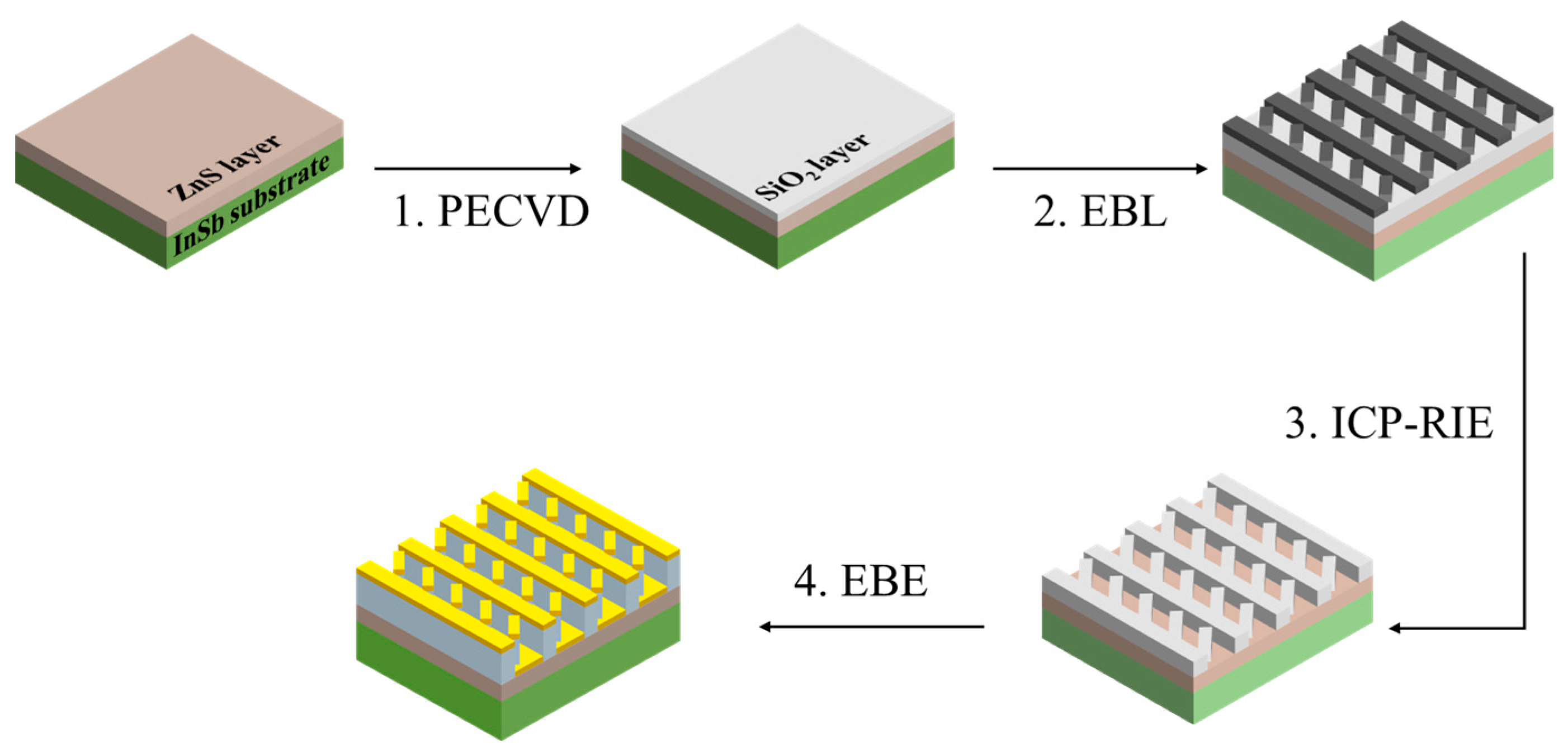
2. Materials and Methods

Figure 1a presents a schematic diagram of the designed three-layer complementary chiral metasurface (TCCM) structure array, where circularly polarized light is incident perpendicular to the -z axis. The TCCM structure consists of three layers. The first layer is an aluminum (Al) metal nanoslit layer with a thickness of h4. The second layer is a patterned dielectric layer of silicon dioxide (SiO2) with a thickness of h3. The third layer is a nanorod layer, also made of Al, with a thickness of h4. The combination of the nanoslit layer and the nanorod layer forms a complementary chiral structure. As shown in Figure 1b, the entire TCCM structure is directly integrated onto an InSb substrate with a thickness of h1. InSb is a typical mid-infrared (3–5 μm) photodetector material. Prior to the integration of the TCCM, a passivation layer of zinc sulfide (ZnS) with a thickness of h2 is deposited. The passivation layer serves to protect the InSb material from oxidation. As shown in Figure 1c, the nanorod layer in the TCCM structure consists of two types of rods: vertical rectangular rods and tilted rectangular rods. The width of the tilted rectangular rods is a, the length is b, and the tilt angle is α. These geometric parameters are carefully designed to align the electric field in a specific manner to achieve the desired circular polarization resolution characteristics. The vertical rectangular rods have a width of ω, a length of Py, and a spacing of g. The nanoslit layer structure complements the nanorod layer structure, with structural parameters as shown in Figure 1d. This complementary relationship between the nanoslit layer and the nanorod layer is a key design feature of the TCCM, enabling the TCCM structure to distinguish between LCP and RCP light in the 2–6 μm wavelength range. The unit cell of the TCCM has a periodicity of Px and Py in the x and y directions, respectively.
In this study, we use the finite-difference time-domain (FDTD) method to simulate the TCM. The simulation area is set as a periodic boundary in the x and y directions and a perfect absorbing layer (PML) in the z-direction. The transmittance monitor is placed at the contact surface of the InSb and ZnS layers. The refractive index parameters of SiO2 are built in by the software, and those of InSb, ZnS, and Al are obtained from the reference [29,30,31]. In the subsequent calculations, the structural parameters were set as a = 0.1 μm, b = 1 μm, α = 45°, Px = 1.6 μm, Py = 1 μm, g = 1.2 μm, ω = 0.2 μm, λ = 2–6 μm, h1 = 1 μm, h2 = 0.35 μm, h3 = 0.2 μm, and h4 = 0.05 μm. The CD is defined as follows in this paper:
CD = T LCP   -   T RCP
where TLCP and TRCP are the transmittance of LCP light and RCP light arriving at the transmittance monitoring interface through the TCCM.

3. Results and Analysis

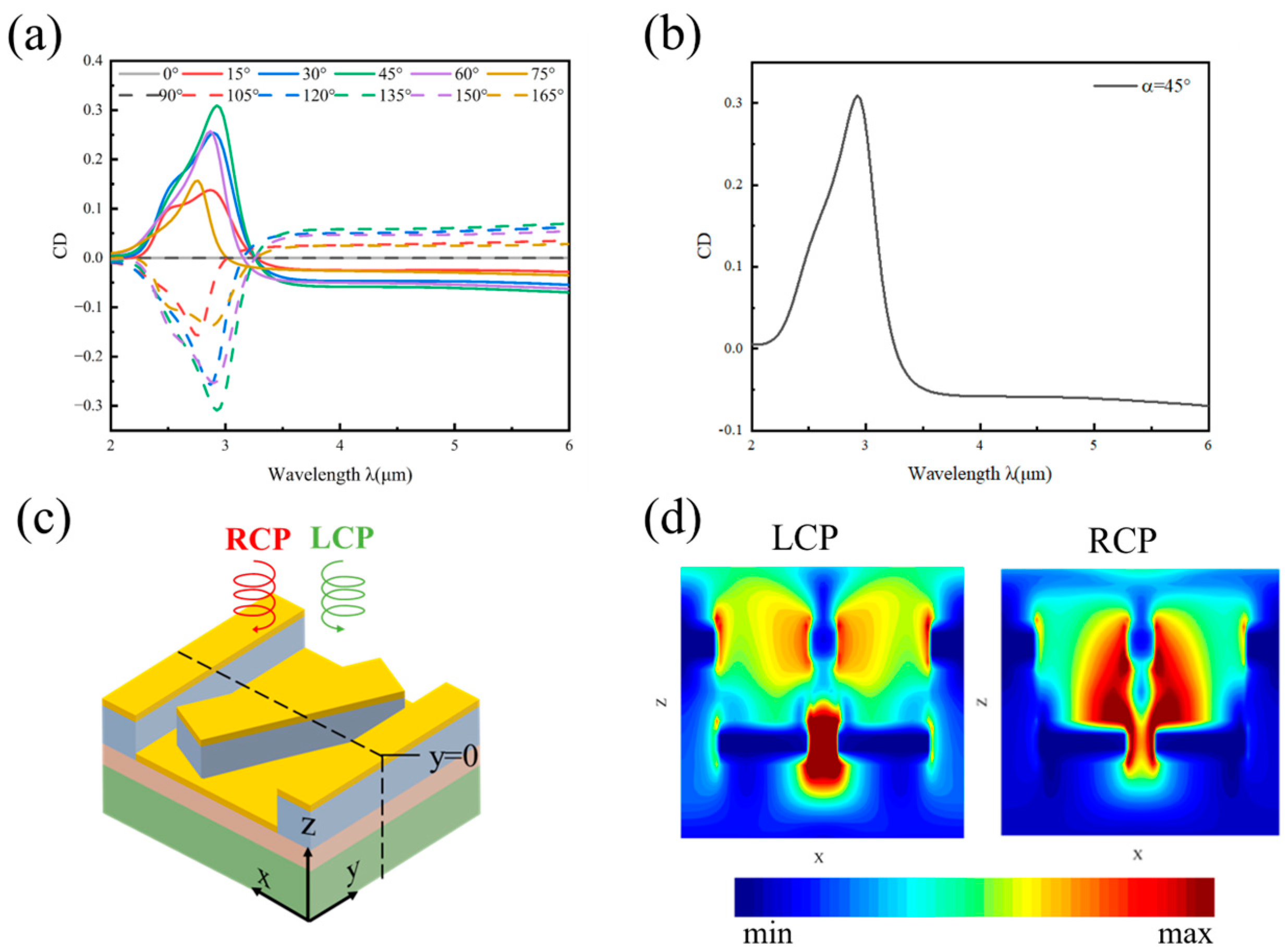
3.1. Tilted Rectangular Bars Produce Symmetry-Breaking
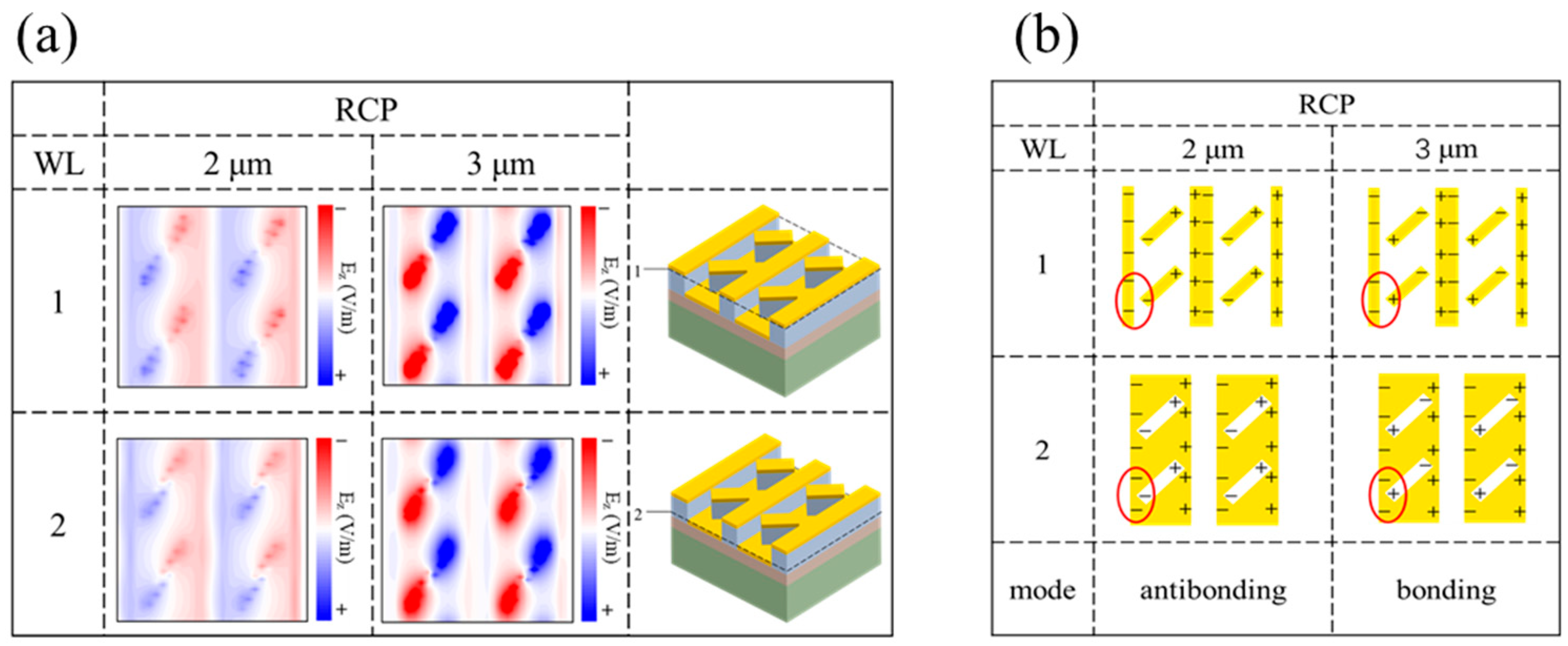
The tilt angle α of the tilted rectangular bar is the main source of the CD effect. When α is neither 0° nor 90°, the TCCM structure is chiral. In order to investigate the intrinsic relationship between the tilt angle α and the CD optical response, we have calculated the CD spectra for α increasing from 0° to 165°. From the spectra obtained, it can be clearly seen that the peaks of the CD spectra show a tendency to increase and then decrease, reaching a maximum value at α = 45°. This phenomenon is due to the fact that when the tilted rectangular bar is tilted at an angle of α ≠ 0°/90°, it breaks the original symmetry of the structure and introduces symmetry breaking, which makes the TCCM behave as a chiral structure. Meanwhile, it is worth noting that the CD values of α between 0° and 90° and α between 90° and 180° have opposite signs and are approximately symmetric along the zero axis from the CD spectra. Based on this, we define TCCMs with tilt angles of α and α + 90° as chiral counterparts, and the CD values of the chiral counterparts have opposite signs and equal absolute values. In view of the important finding that the maximum value of the CD spectra occurs at α = 45°, in the following study, we set α = 45° and kept it constant without any special specification of the remaining parameters. From Figure 2a, it is clear that the CD spectrum reaches a maximum near the wavelength of 3 μm at α = 45°.
To further investigate the influence of the TCCM structure on the transmission of circularly polarized light, we calculated the transmission spectra of α = 45° LCP light and RCP light, and the results are shown in Figure 2b, from which it can be seen that the RCP light has a very small value near 3 µm. We then calculated the electric field distributions of the LCP light and the RCP light in the x-z plane at y = 0 for a wavelength of 2.928 µm, where the calculated position of the x-y plane is shown in Figure 2c, and the results of the electric field distributions are shown in Figure 2d. From Figure 2d, it can be clearly seen that under LCP light excitation, the electric field resonance of the TCCM mainly occurs within the nanoslit, while under RCP light resonance excitation, the transmission of the TCCM mainly occurs between the nanorods and the nanoslit membrane. The different electric fields excited by different circularly polarized light resulted in different circularly polarized light transmittances, which in turn affected the CD.

3.2. Coupling Mode

To investigate the physical mechanism behind the CD effect of the TCCM structure, we calculate the Ez component distribution of the near-field electric field in the x-y planes at λ = 2 μm and λ = 3 μm for the upper surface of the nanoslit and the lower surface of the nanorod, where the Ez component represents the charge density distribution.
Figure 3a shows the electric field distribution that we can observe between the upper and lower metal layers of the TCCM structure under the LCP light excitation at λ = 2 μm: different charge distributions are excited between the adjacent edges and corners of the vertical rectangular bar and the adjacent tilted rectangular bar, as well as at the upper corners of the rectangular nanoslits on the lower nanoslit film and at the adjacent film edges. In contrast, during LCP photoexcitation at λ = 3 μm, the same charge distribution was excited between the adjacent edges and corners of the upper vertical rectangular bar and the adjacent tilted rectangular bar, as well as at the upper corners of the rectangular nanoslits on the lower nanoslit film and at the adjacent film edges. A sketch of the corresponding charge distribution is shown in Figure 3b. It is convenient for us to understand this more intuitively.
As shown in Figure 4a, the electric field distribution of the TCCM structure under RCP light excitation at λ = 2 μm reveals that the same charge distribution is excited between the adjacent edges and corners of the vertical rectangular bar and the adjacent tilted rectangular bar, as well as at the upper corners of the rectangular nanoslits on the nanoslit film and at the adjacent edges of the film. However, under RCP light excitation at λ = 3 μm, different charge distributions are excited at these positions. The corresponding charge distribution is shown in Figure 4b.
We attribute the above charge distribution phenomenon to the fact that different circularly polarized light excites different binding modes on the TCCM structure. Such binding modes are divided into low energy binding modes and high energy antibonding modes. Among them, the antibonding mode is formed by the accumulation of charges of the same sign on the adjacent rod corners, while the bonding mode is formed by the opposite charges on the adjacent rod corners.
As shown in Figure 2b, at 2 μm, the transmittance of LCP light is less than that of RCP light; at 3 μm, the transmittance of LCP light is greater than that of RCP light. Combined with the charge distributions shown in Figure 3 and Figure 4, further analysis shows that the LCP light at 2 μm excites the bonding mode, and the RCP light excites the antibonding mode in the TCCM structure; the LCP light at 3 μm excites the antibonding mode, and the RCP light excites the bonding mode. Due to the different effects of the two modes on the circularly polarized transmission, this ultimately leads to the difference in transmission of the left- and right-spin circularly polarized light. For the TCCM structure, the transmission in the bonding mode is lower than that in the antibonding mode.

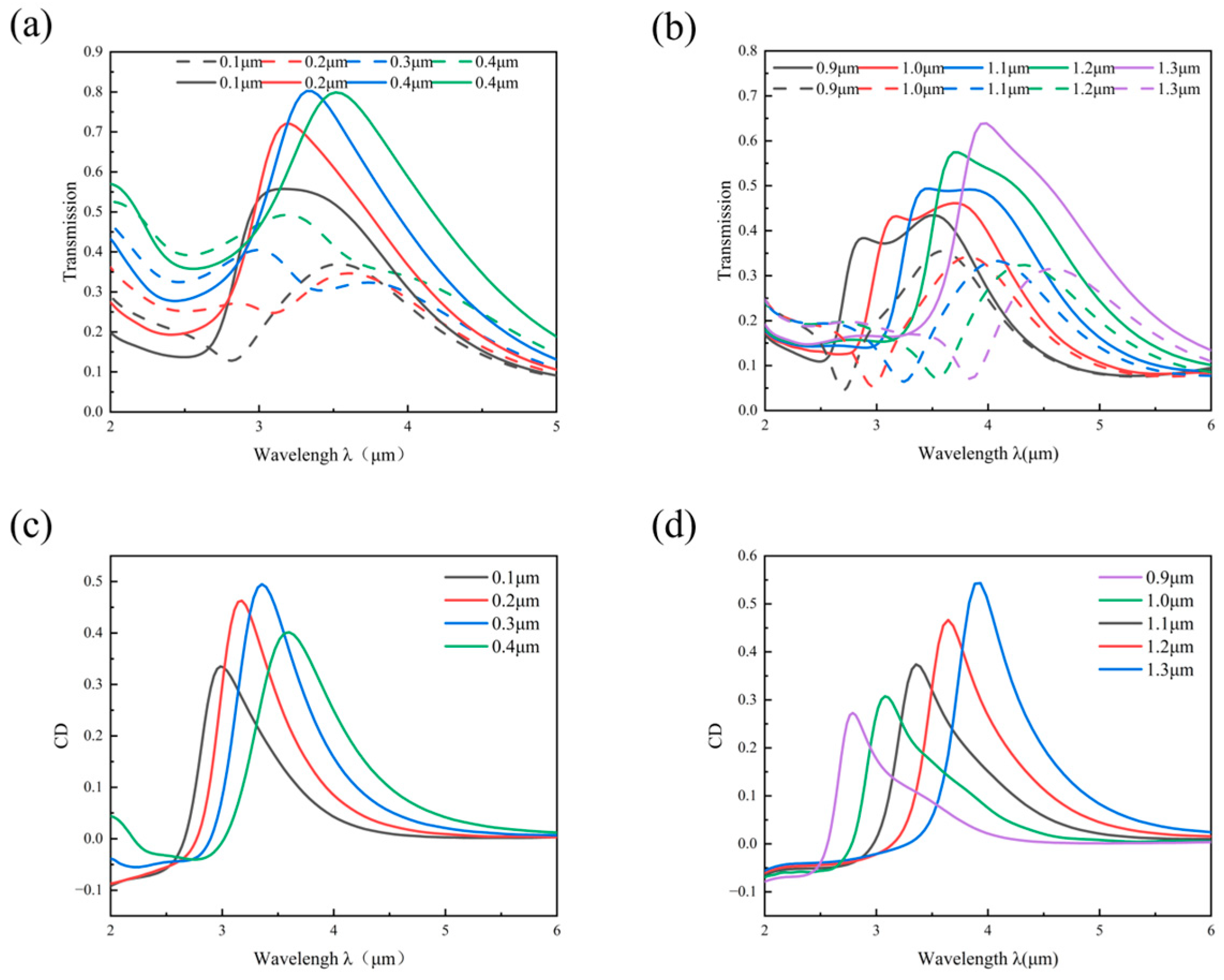
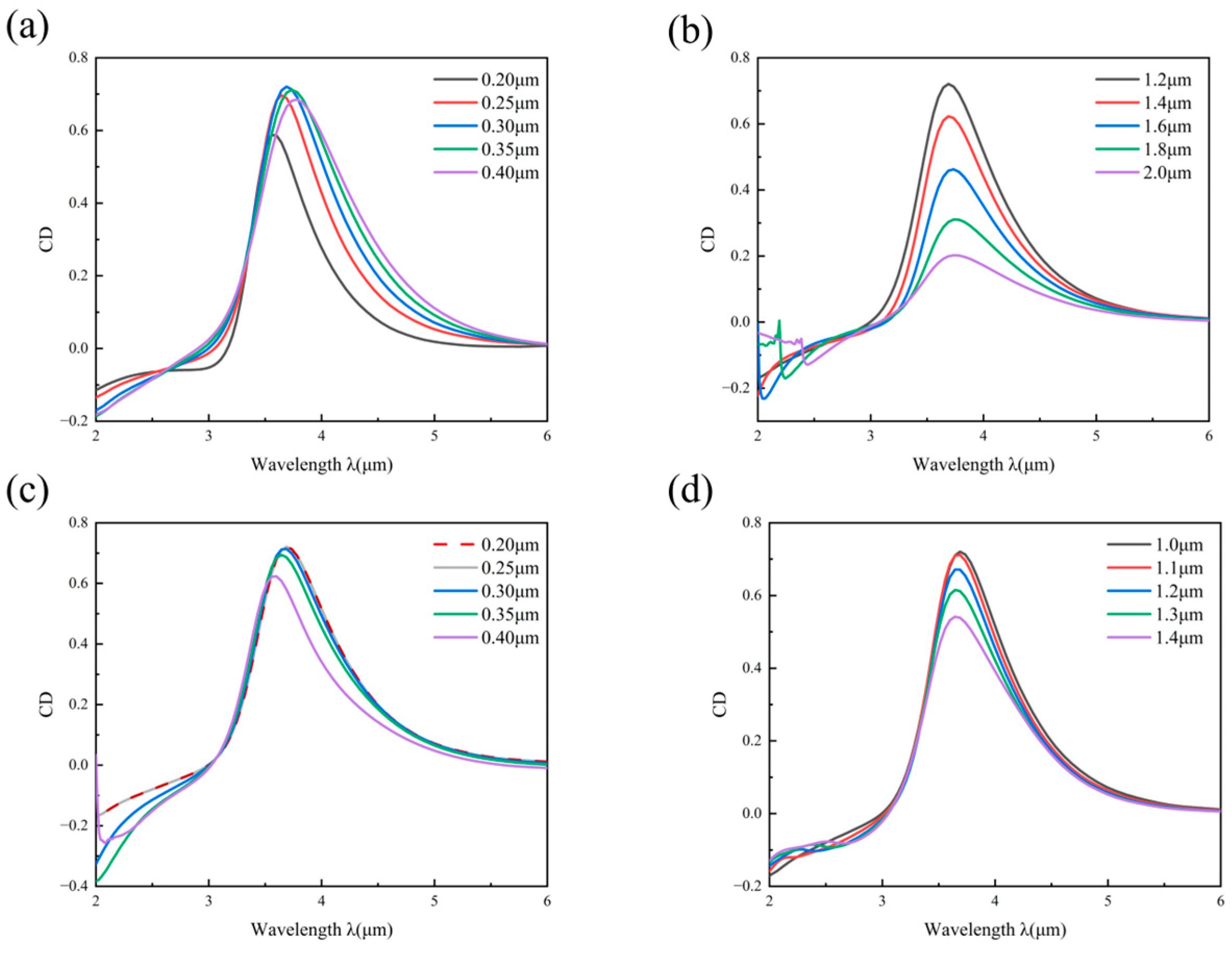
3.3. Structural Optimization

The near-field coupling between nanostructures is closely related to the geometrical parameters of nanostructures [32,33,34]. In order to investigate the influence of the TCCM structural parameters on the CD effect, we systematically varied each parameter individually. Figure 5a shows the transmittance spectra of LCP light and RCP light when parameter a is changed from 0.1 μm to 0.4 μm while keeping the other parameters constant. From the figure, it is clearly seen that the transmittance spectra are red-shifted in the transmission peak with the increase in parameter a, while the TLCP peak first increases and then decreases. Figure 5b shows the transmittance spectra when parameter b is changed from 0.9 μm to 1.3 μm while keeping the other parameters constant. From the figure, it is clearly seen that the transmittance spectra are red-shifted in the transmission peak with increasing parameter b, while the TLCP increases significantly. Figure 5c shows the CD spectra when parameter a is changed from 0.1 μm to 0.4 μm while keeping the other parameters constant. The peaks of the CD spectra of the TCCM structure exhibit an increase and then a decrease in the range of a = 0.1 μm to 0.4 μm. It is mainly because with the increase in parameter a, the transmittance of LCP and RCP light increases, leading to the increase in CD, but with the further increase in parameter a, the nanoslit becomes larger, and the electromagnetic coupling strength between the nanoslit weakens, leading to the weakening of the TCCM’s ability to limit the transmittance of RCP light. Therefore, it can be seen that the variation of parameter a mainly affects the transmittance of RCP light. Figure 5d shows the CD spectra when parameter b is changed from 0.9 μm to 1.3 μm while keeping the other parameters constant. It can be clearly seen that the CD spectra gradually increase the peak of the CD spectra with the increase in parameter b. This is mainly due to the fact that the electromagnetic coupling between neighboring nanorods and between neighboring nanoslits is enhanced with the increase in parameter b, resulting in a weaker limitation of the transmission of LCP light by the TCCM. Therefore, it can be seen that the variation of parameter b mainly affects the transmittance of LCP light. The variation of parameters a and b induces a red-shift of the peak of the CD spectrum, a phenomenon that can be attributed to the different resonance wavelengths associated with the excitation of the equipolar exciton. Surface-isolated polarized excitations (SPP) are electromagnetic excitation modes that propagate along the interface between a dielectric and a conductor [35,36]. The surface-isolated exciton resonance is caused by the resonance between exponentially decaying surface fast-wave electromagnetic waves and the isolated exciton polarized exciton on the metal surface. Based on the above results, we can achieve high CD values and tunable peak CD spectral response wavelengths in the 2–6 μm band by reasonably adjusting the values of parameters a and b. We set the parameters a = 0.25 μm and b = 1.1 μm in the subsequent calculations according to the practical requirements, and the rest of the parameter settings remain unchanged if not otherwise specified.
Figure 6a shows the CD spectra when the parameter h3 is increased from 0.2 μm to 0.4 μm while keeping other parameters constant. It is evident that, with the increase in h3, the peak of the CD spectra initially increases and then decreases. This occurs primarily because when the parameter h3 is too small, the proximity between the Al nanocrystalline thin film and Al nanorods decreases. This reduced spacing brings the TCCM closer to the metal plane, ultimately leading to reduced transmission efficiency. If the distance between the Al slit film and the Al nanorods is too large, the near-field coupling between the Al slit film and the nanorods becomes weaker, resulting in a lower CD value. The parameter h3 = 0.3 μm is set in the subsequent calculations, and the rest of the parameter settings are kept unchanged unless otherwise specified. Figure 6b shows the CD spectra when the parameter g is increased from 1.2 μm to 2.0 μm (note: since g increases, this leads to an increase in Px, so here the magnitude of Px varies with the increase in parameter g, and the rest of the parameters are kept constant). As parameter g increases, the vertical and tilted rectangular bars become more widely spaced, and the electric field coupling becomes weaker, leading to a decrease in the peak CD spectra (the peak of the CD spectrum is reduced from 0.72 to 0.2 in the 2–6 μm range). The parameter g = 1.2 μm is used in the subsequent calculations, and the rest of the parameter settings remain constant unless otherwise specified.
Figure 6c shows the CD spectra as the structural parameter ω increases from 0.2 μm to 0.4 μm. Since ω increases while g remains constant, this results in an increase in Px. Therefore, the magnitude of Px varies with ω, while other parameters remain unchanged. The gradual decrease in the peak CD spectra with increasing ω is attributed to the widening of the vertical nanoslit, which weakens the electric field coupling and reduces the confinement of RCP light, leading to a smaller CD. Figure 6d presents the CD spectra as the structural parameter Py increases from 1 μm to 1.4 μm while keeping other parameters constant. The figure shows that the peak of the CD spectra decreases as Py increases. This can be explained by the larger spacing between adjacent tilted nanoslits, which weakens the electric field coupling. As illustrated in the charge distribution in Figure 3, mutual coupling exists between neighboring tilted nanorods and between neighboring tilted nanoslits along the y-axis. However, as Py increases, the coupling distance increases, leading to a weaker electric dipole moment. This reduction in dipole strength results in a decrease in the peak CD spectra.

4. Discussion

The CD value of the optimized TCCM structure can reach 0.72 in the 2–6 μm band. Although this result is still far from the 0.9 CD value of Bai et al. [21], it is higher than the 0.62 CD value of Zuo et al. [23]. This shows that the TCCM structure provides a feasible solution for the integration of chiral metasurface chips. At the same time, the TCCM structure is easy to integrate on-chip, which is conducive to future applications. As shown in Figure 7, the recommended process steps include: 1. Deposition of the SiO2 layer on the InSb substrate by plasma-enhanced chemical vapor deposition (PECVD); 2. Pattern transfer by electron beam lithography (EBL); 3. The patterned SiO2 dielectric layer was constructed using an inductively coupled plasma reactive ion etching (ICP-RIE) apparatus; 4. The first and third patterned metal layers are deposited simultaneously by electron beam evaporation (EBE). Compared with traditional multilayer chiral metasurfaces [22,23,24], the TCCM structure offers significant advantages: it eliminates multiple lithography and deposition steps, greatly simplifying the fabrication process. The top and bottom metal layers are constructed simultaneously, eliminating the need for layer-by-layer processing and high-precision alignment, effectively avoiding alignment errors and significantly improving manufacturability. In the mass production stage, replacing electron beam lithography with nanoimprint technology can further enhance production efficiency [37].

5. Conclusions

In conclusion, we have introduced a three-layer complementary chiral metasurface (TCCM) that achieves a circular dichroism (CD) value of up to 0.72 in the 2–6 μm wavelength range. FDTD simulation results show that the electric fields excited by left-handed circularly polarized (LCP) and right-handed circularly polarized (RCP) light on the TCCM structure exhibit different bonding modes (bonding and antibonding), which is the fundamental mechanism of the observed CD response. We have systematically optimized the geometric parameters of the TCCM structure, further enhancing the CD value. Compared to existing multi-layer designs that require complex lithography techniques, the proposed TCCM significantly reduces manufacturing steps and complexity in the context of on-chip integration. This work provides a feasible solution for applications in mid-infrared light communication, real-time polarization imaging, and chiral sensing.

Author Contributions

Conceptualization, J.X., J.L. and R.H.; data curation, G.C. and W.W.; formal analysis, H.L. and P.S.; funding acquisition, R.H.; investigation, H.L. and P.S.; methodology, J.X., J.L., G.C. and W.W.; resources, Y.L. and J.K.; software, J.X. and J.L.; supervision, R.H. and J.Z.; validation, Y.L., J.K. and J.Z.; visualization, J.X. and J.L.; writing—original draft, J.X. and J.L.; writing—review and editing, R.H. and J.Z. All authors have read and agreed to the published version of the manuscript.

Funding

Aeronautical Science Foundation of China (20240024036001); the open subject of the National Key Laboratory of Infrared Detection Technologies (Grant No. IRDT-23-02, Grant No. 2024-JJ-103-02); Yunnan Science and Technology Program Projects (2023032A08001).

Institutional Review Board Statement

Not applicable.

Informed Consent Statement

Not applicable.

Data Availability Statement

Data underlying the results presented in this paper are not publicly available at this time but may be obtained from the authors upon reasonable request.

Conflicts of Interest

The authors declare no conflicts of interest.

References

  1. Lee, Y.H.; Won, Y.; Mun, J.; Lee, S.; Kim, Y.; Yeom, B.; Dou, L.; Rho, J.; Oh, J.H. Hierarchically Manufactured Chiral Plasmonic Nanostructures with Gigantic Chirality for Polarized Emission and Information Encryption. Nat. Commun. 2023, 14, 7298. [Google Scholar] [CrossRef] [PubMed]
  2. Liu, S.; Wang, X.; Ni, J.; Cao, Y.; Li, J.; Wang, C.; Hu, Y.; Chu, J.; Wu, D. Optical Encryption in the Photonic Orbital Angular Momentum Dimension via Direct-Laser-Writing 3D Chiral Metahelices. Nano Lett. 2023, 23, 2304–2311. [Google Scholar] [CrossRef] [PubMed]
  3. Gassó, S.; Knobelspiesse, K.D. Circular Polarization in Atmospheric Aerosols. Atmos. Chem. Phys. 2022, 22, 13581–13605. [Google Scholar] [CrossRef]
  4. He, C.; He, H.; Chang, J.; Chen, B.; Ma, H.; Booth, M.J. Polarisation Optics for Biomedical and Clinical Applications: A Review. Light Sci. Appl. 2021, 10, 194. [Google Scholar] [CrossRef]
  5. Long, G.; Sabatini, R.; Saidaminov, M.I.; Lakhwani, G.; Rasmita, A.; Liu, X.; Sargent, E.H.; Gao, W. Chiral-Perovskite Optoelectronics. Nat. Rev. Mater. 2020, 5, 423–439. [Google Scholar] [CrossRef]
  6. Wang, C.; Cheng, X.; Wang, R.; Hu, X.; Wang, C. Flexibly Designable 2D Chiral Metasurfaces with Pixelated Topological Structure Based on Machine Learning. Laser Photonics Rev. 2024, 18, 2300958. [Google Scholar] [CrossRef]
  7. Lee, G.J.; Cho, M.J.; Choi, E.H.; Choi, D.H. Optical Sensing of Chiral Polymer Thin Films. In Computational Optical Sensing and Imaging; Optica Publishing Group: Washington, DC, USA, 2020. [Google Scholar]
  8. Huang, Z.; Wang, J.; Jia, W.; Zhang, S.; Zhou, C. Controllable Perfect Chiral Optical Response in Planar Metasurfaces Empowered by Quasi-Bound States in the Continuum. Opt. Express 2024, 32, 33029. [Google Scholar] [CrossRef]
  9. Qu, Y.; Lei, L.; Yu, Y.; Zhang, X.; Qian, Z. Coexistence of Circular Dichroism and Asymmetric Transmission in Babinet-Complementary Metamaterials. Opt. Express 2022, 30, 30394. [Google Scholar] [CrossRef]
  10. Qu, Y.; Zhang, Y.; Wang, F.; Li, H.; Ullah, H.; Aba, T.; Wang, Y.; Fu, T.; Zhang, Z. A General Mechanism for Achieving Circular Dichroism in a Chiral Plasmonic System. Ann. Phys. 2018, 530, 1800142. [Google Scholar] [CrossRef]
  11. Yang, Z.Y.; Zhao, M.; Lu, P.X.; Lu, Y.F. Ultrabroadband Optical Circular Polarizers Consisting of Double-Helical Nanowire Structures. Opt. Lett. 2010, 35, 2588. [Google Scholar] [CrossRef]
  12. Zhang, J.; Guo, Z.; Zhou, K.; Ran, L.; Zhu, L.; Wang, W.; Sun, Y.; Shen, F.; Gao, J.; Liu, S. Circular Polarization Analyzer Based on an Archimedean Nano-Pinholes Array. Opt. Express 2015, 23, 30523. [Google Scholar] [CrossRef] [PubMed]
  13. Kang, L.; Wang, C.-Y.; Guo, X.; Ni, X.; Liu, Z.; Werner, D.H. Nonlinear Chiral Meta-Mirrors: Enabling Technology for Ultrafast Switching of Light Polarization. Nano Lett. 2020, 20, 2047–2055. [Google Scholar] [CrossRef] [PubMed]
  14. Mahmud, M.S.; Rosenmann, D.; Czaplewski, D.A.; Gao, J.; Yang, X. Chiral Plasmonic Metasurface Absorbers in the Mid-Infrared Wavelength Range. Opt. Lett. 2020, 45, 5372. [Google Scholar] [CrossRef] [PubMed]
  15. Cotrufo, M.; Osorio, C.I.; Koenderink, A.F. Spin-Dependent Emission from Arrays of Planar Chiral Nanoantennas Due to Lattice and Localized Plasmon Resonances. ACS Nano 2016, 10, 3389–3397. [Google Scholar] [CrossRef]
  16. Hwang, Y.; Lee, S.; Kim, S.; Lin, J.; Yuan, X.-C. Effects of Fano Resonance on Optical Chirality of Planar Plasmonic Nanodevices. ACS Photonics 2018, 5, 4538–4544. [Google Scholar] [CrossRef]
  17. Zu, S.; Bao, Y.; Fang, Z. Planar Plasmonic Chiral Nanostructures. Nanoscale 2016, 8, 3900–3905. [Google Scholar] [CrossRef]
  18. Shen, Z.; Lin, X.; Huang, D. Dual-Mode Dual-Band Circular Polarization Device Based on Three-Layer Plasmonic Metasurface. APL Mater. 2023, 11, 091108. [Google Scholar] [CrossRef]
  19. Mutlu, M.; Ozbay, E. A Transparent 90° Polarization Rotator by Combining Chirality and Electromagnetic Wave Tunneling. Appl. Phys. Lett. 2012, 100, 51909. [Google Scholar] [CrossRef]
  20. Tanaka, K.; Arslan, D.; Fasold, S.; Steinert, M.; Sautter, J.; Falkner, M.; Pertsch, T.; Decker, M.; Staude, I. Chiral Bilayer All-Dielectric Metasurfaces. ACS Nano 2020, 14, 15926–15935. [Google Scholar] [CrossRef]
  21. Bai, J.; Yao, Y. Highly Efficient Anisotropic Chiral Plasmonic Metamaterials for Polarization Conversion and Detection. ACS Nano 2021, 15, 14263–14274. [Google Scholar] [CrossRef]
  22. Wang, C.; Wang, R.; Cheng, X.; Hu, X.; Wang, C. Passively Broadband Tunable Dual Circular Dichroism via Bound States in the Continuum in Topological Chiral Metasurface. ACS Nano 2024, 18, 18922–18932. [Google Scholar] [CrossRef] [PubMed]
  23. Zuo, J.; Bai, J.; Choi, S.; Basiri, A.; Chen, X.; Wang, C.; Yao, Y. Chip-Integrated Metasurface Full-Stokes Polarimetric Imaging Sensor. Light: Sci. Appl. 2023, 12, 218. [Google Scholar] [CrossRef] [PubMed]
  24. Wang, Q.; Bao, J.; Liu, L.; Yang, Y.; Yang, J.; Gao, H.; Liu, T.; Dong, H.; Wu, Y.; Zhang, Y.; et al. High-Performance near-Infrared Narrowband Circularly Polarized Light Organic Photodetectors. Nano Today 2024, 54, 102132. [Google Scholar] [CrossRef]
  25. You, X.; Ako, R.T.; Bhaskaran, M.; Sriram, S.; Fumeaux, C.; Withayachumnankul, W. Mechanically Tunable Terahertz Circular Polarizer with Versatile Functions. Laser Photonics Rev. 2023, 17, 2200305. [Google Scholar] [CrossRef]
  26. Zhang, G.; Lyu, X.; Qin, Y.; Li, Y.; Fan, Z.; Meng, X.; Cheng, Y.; Cao, Z.; Xu, Y.; Sun, D.; et al. High Discrimination Ratio, Broadband Circularly Polarized Light Photodetector Using Dielectric Achiral Nanostructures. Light. Sci. Appl. 2024, 13, 275. [Google Scholar] [CrossRef]
  27. Wu, Y.; Shen, Y.; Addamane, S.; Reno, J.L.; Williams, B.S. Tunable Quantum-Cascade VECSEL Operating at 1.9 THz. Opt. Express 2021, 29, 34695. [Google Scholar] [CrossRef]
  28. Shen, Y.; Kim, A.D.; Shahili, M.; Curwen, C.A.; Addamane, S.; Reno, J.L.; Williams, B.S. THz Time-Domain Characterization of Amplifying Quantum-Cascade Metasurface. Appl. Phys. Lett. 2021, 119, 181108. [Google Scholar] [CrossRef]
  29. Adachi, S. Optical Dispersion Relations for GaP, GaAs, GaSb, InP, InAs, InSb, AlxGa1−xAs, and In1−xGaxAsyP1−y. J. Appl. Phys. 1989, 66, 6030–6040. [Google Scholar] [CrossRef]
  30. Amotchkina, T.; Trubetskov, M.; Hahner, D.; Pervak, V. Characterization of E-Beam Evaporated Ge, YbF3, ZnS, and LaF3 Thin Films for Laser-Oriented Coatings. Appl. Opt. 2020, 59, A40. [Google Scholar] [CrossRef]
  31. Ordal, M.A.; Bell, R.J.; Alexander, R.W.; Newquist, L.A.; Querry, M.R. Optical Properties of Al, Fe, Ti, Ta, W, and Mo at Submillimeter Wavelengths. Appl. Opt. 1988, 27, 1203. [Google Scholar] [CrossRef]
  32. Tabor, C.; Van Haute, D.; El-Sayed, M.A. Effect of Orientation on Plasmonic Coupling between Gold Nanorods. ACS Nano 2009, 3, 3670–3678. [Google Scholar] [CrossRef]
  33. Shi, Y.; Zhang, W. Characterizing Chiroptical Properties of 2D/3D Structures Based on an Improved Coupled Dipole Theory. Opt. Express 2024, 32, 10046. [Google Scholar] [CrossRef]
  34. Tang, H.; Rosenmann, D.; Czaplewski, D.A.; Yang, X.; Gao, J. Dual-Band Selective Circular Dichroism in Mid-Infrared Chiral Metasurfaces. Opt. Express 2022, 30, 20063. [Google Scholar] [CrossRef]
  35. Maier, S.A. Plasmonics: Fundamentals and Applications; Springer: New York, NY, USA, 2007; ISBN 978-0-387-33150-8. [Google Scholar]
  36. Li, H.; Hao, R.; Chen, G.; Wang, W.; Sheng, P.; Xu, J.; Liu, J.; Li, Y.; Kong, J.; Zhao, J. Optimization of the Inverted “T”-Shaped Double-Layer Subwavelength Grating Design Integrated on an InSb Detector. Opt. Commun. 2024, 573, 131016. [Google Scholar] [CrossRef]
  37. Choi, S.; Zuo, J.; Das, N.; Yao, Y.; Wang, C. Scalable Nanoimprint Manufacturing of Functional Multilayer Metasurface Devices. Adv. Funct. Mater. 2024, 34, 2404852. [Google Scholar] [CrossRef]
Figure 1. (a) Array and unit diagram of TCCM structure. (b) Schematic diagram of TCCM cell structure with InSb substrate. (c) Unit structure parameters of the TCCM rectangular rod layer. (d) Unit structure parameters of the TCCM nanoslit layer.
Photonics 12 00228 g001
Figure 2. (a) CD spectra when the tilt angle α is varied in the range of 0°–165°. (b) Transmission spectra of LCP and RCP light at α = 45°. (c) Structure of the TCCM cell at α = 45°, with the dashed line indicating the position of the x-z plane at y = 0. (d) Electric field distribution of LCP and RCP light in the x-z plane at y = 0 at λ = 2.928 μm, with the color bar indicating the electric field strength.
Photonics 12 00228 g002
Figure 3. (a) The electric field distribution of the Ez component in the x-y plane for the first and third layers of the TCCM structure under LCP light excitation at wavelengths of 2 μm and 3 μm. (b) Schematic representation of the charge distribution in the x-y plane for the first and third layers of the TCCM structure under identical conditions.
Photonics 12 00228 g003
Figure 4. (a) The electric field distribution of the Ez component in the x-y plane for the first and third layers of the TCCM structure under RCP light excitation at wavelengths of 2 μm and 3 μm. (b) Schematic representation of the charge distribution in the x-y plane for the first and third layers of the TCCM structure under identical conditions.
Photonics 12 00228 g004
Figure 5. (a) The transmission spectrum of parameter a ranges from 0.1 μm to 0.4 μm, with TLCP as the solid line and TRCP as the dashed line. (b) Transmittance spectra of parameter b varying from 0.9 μm to 1.3 μm, with the solid line indicating TLCP and the dashed line indicating TRC. (c) CD spectra of parameter a varying from 0.1 μm to 0.4 μm. (d) CD spectra with parameter b varying from 0.9 μm to 1.3 μm.
Photonics 12 00228 g005
Figure 6. (a) CD spectra of parameter h3 varying from 0.2 μm to 0.4 μm. (b) CD spectra with parameter g varied from 1.2 μm to 2.0 μm. (c) CD spectra with parameter ω varied from 0.2 μm to 0.4 μm (d) CD spectra with parameter Py varied from 1.0 μm to 1.4 μm.
Photonics 12 00228 g006
Figure 7. Recommended fabrication process of on-chip integrated TCCM structure.
Photonics 12 00228 g007
Disclaimer/Publisher’s Note: The statements, opinions and data contained in all publications are solely those of the individual author(s) and contributor(s) and not of MDPI and/or the editor(s). MDPI and/or the editor(s) disclaim responsibility for any injury to people or property resulting from any ideas, methods, instructions or products referred to in the content.

