1. Introduction
Since its discovery by William Henry Fox Talbot in 1836 [
1], inherent self-imaging in a lens-less environment has contributed to a variety of applications [
2,
3,
4,
5,
6,
7,
8]; and much research is still in progress to extract and utilize its potential. Since its inception as a feature of free-space diffraction from a grating, early studies concentrated on the physical explanation and obtaining insight into the phenomenon. Lord Rayleigh calculated the Talbot length required for single self-image formation [
9]; Cowley and Moodie adopted the term ‘Fourier image’ for this exact self-image [
10], whereas the Fresnel images formed by the Fresnel diffraction in between these Fourier image planes were studied by Winthrop and Worthington [
11]. More recently, Berry and Klein [
12], using a modern treatment, found the irreducible number-theoretic expressions for the phase in planes located at rational fractions of the Talbot length and the fractal intensity distributions at the planes located at irrational fractions of the Talbot length, needed for a complete description of a Talbot carpet beyond the initial field.
The substantial potential of the Talbot effect can be explored more extensively for a field propagating in an engineered material. Examples include exploiting the anisotropy and spatial dispersion of a metamaterial in the form of a longitudinally multi-slotted MMI multimode waveguide region of an MMI [
13] or transverse subwavelength structure [
14].
Self-imaging within a waveguide was first suggested by Bryngdahl [
15]. Ulrich and Ankele performed a demonstration of the formation of single and multiple self-images in multimode optical waveguides with homogenous refractive index [
16], which initiated the extensive incorporation of this phenomenon into diverse applications. The MMI coupler is a popular implementation of the spatial Talbot effect [
2], which has contributed components with a variety of functions [
3,
4,
17,
18,
19,
20,
21,
22]. Other sectors, such as optoelectronics [
5,
23], sensors [
6,
24,
25,
26,
27,
28], optical metrology [
7], discrete sine and cosine transform networks [
29], and broadening spectral response of AWG demultiplexer [
30] employ Talbot effect in multimode waveguide. Recent studies on the temporal Talbot effect for controlling the optical pulse train repetition rate [
8], the spectral Talbot effect for achieving comb-free spectral range [
31], and their unification for noise reduction and passive amplification of an optical signal [
32,
33,
34], and a generalized angle-OAM Talbot effect and its application in OAM-based information processing [
35], show how the Talbot effect is at the conceptual heart of many diverse devices, systems, and physical phenomena.
The transmission matrix is a simple, compact means to describe the transmission of a multi-port device with negligible backscattering. Heaton et al. [
36] first introduced a transmission matrix description of MMIs. Recently, Nikkhah et al. [
37] have revisited the problem of establishing the natural connection between the free-space Talbot matrix and the MMI transmission matrix. The physical implementations for the free-space and waveguide Talbot effects are fundamentally distinct. Nikkhah et al. [
37] showed how the anti-symmetry caused by the multimode region waveguide sidewalls results in a model that imitates a free equivalent. This enables the formulation of integer and fractional Talbot effect in free space, developed by Berry et al. [
12], to be followed to construct the free-space Talbot transmission matrix, which is then mapped into the multimode waveguide Talbot transmission matrix. In addition to obtaining the correct amplitude and relative phase factors between a lattice of point sources and their self-images on a transverse plane at integer or rational fractional multiples of Talbot distances, the mapping also describes how the symmetry properties of an MMI coupler transmission matrix are inherited from the free-space Talbot structure. Nikkhah et al. [
37] focused their work on the transmission matrix of the most deployed MMI type I geometry. This paper elaborates further on the type I geometry to present additional features. In addition, the derivation of the transmission matrix is extended to a second type II geometry that offers distinct features such as a sparse transmission matrix, omission of ports without any power penalty, couplers with unequal splitting ratios, flexibility in access port position along the transverse plane and many interesting, unconventional MMI structures with closed form amplitude–phase characteristics. One of them is the
MMI coupler with golden splitting ratio.
The golden ratio
has a longer history than the Talbot effect. Its frequent appearance in geometry, number sequences, patterns, and natural objects has attracted both scientific and philosophic attention over the course of history. Euclid defined this irrational number as the number dividing a straight line in the extreme and mean ratio [
38]. Over the centuries, the golden ratio, mostly as a mathematical tool, has been implemented in diverse applications. Some recent studies include, but are not limited to, optimization of golden ratio-based radial profile order for dynamic magnetic resonance imaging (MRI) [
39,
40], implementation of a beta encoder with fractional base
in a Nyquist-rate ADC algorithm [
41,
42], modulation schemes [
43], algorithms for variational inequalities and optimization problems [
44,
45,
46], imaging in two-mirror telescope systems [
47], weak nonlinearity correction in machine learning-enhanced wavelength metering applications [
27], photonic crystal fiber structures for nonlinear optics [
48,
49], and multiple access channel control policies [
50]. To the authors’ knowledge, the natural existence of
as the ratio of the field extrema of the propagation modes in an ensemble of four waveguides organized to form a directional coupler, was first theoretically analyzed by Parriaux [
51].
In this paper, the derivation of a MMI coupler with as its power-splitting ratio between the two output ports is presented. The golden ratio appears spontaneously with a simple MMI structure comparable to the conventional 3 dB MMI coupler and amenable to implementation as a photonic integrated circuit. A standard SOI platform with a 220 nm silicon process has been adopted for the fabrication of the coupler and a Mach–Zehnder interferometric test circuit. Both simulation and experimental results show wideband performance centered at 1550 nm, with nominal deviations, which can be attributed to fabrication limitations.
2. Theory
2.1. Self-Imaging in Free Space and Strongly Confining Multimode Waveguide
William Henry Fox Talbot first observed the repeated self-imaging of a diffraction grating under white light illumination [
1].
Figure 1a shows a simplified setup where a diffraction grating with a period of Λ in the transverse coordinate is illuminated by coherent light in the form of a plane wave. Single self-images are formed in transverse planes at integer multiples of the Talbot distance,
[
9]. For an even integer, the single self-image is a direct replica of the input field. For an odd integer, the single self-image is shifted by a half-period (Λ/2). Following the formulation of the Talbot effect adopted by Berry et al. [
12] and Nikkhah et al. [
37,
52], the initial field
immediately after transmission through the periodic grating structure can be expressed as:
where
is the field over a single transverse period
. Following the treatment in [
12], the field at a transverse plane at z can be represented as:
where the convolution kernel
can be represented by the Poisson sum extended as a solution to the Helmholtz equation:
where
is the lateral wavenumber
and
is the propagation constant. Under the paraxial approximation, the dispersion equation reduces to:
where
. At rational fractional Talbot distances, Equation (3) evaluates to:
where either
is an integer multiple of
resulting in a single self-image of input field at z, or they are coprime integers, resulting in
multiple images with a pitch of
. Equation (5) suggests the introduction of a lattice with pitch
to accommodate the
lateral shift in the images when
is odd. In this way, the Dirac distribution components in Equation (5) occupy the even sites of the lattice when
or
are even and the odd sites when
are odd [
37]. Energy conservation is ensured through the overall amplitude factor
. The overall Talbot phase factor has an unimodular common factor specified by the Gauss quadratic sum [
53] appended by a relative phase factor [
12]:
Here,
signifies the inverse of
modulo
, which can be calculated only if
and
are coprime integers:
The Talbot phase factor is periodic in
and
with integer period
for both, reflecting the transverse period
and longitudinal period
of the field observable in
Figure 1a. A unit circle with 2q regularly spaced points characterized by the singular support of Dirac distribution components on its circumference can be a representation of
because of its periodicity of
. Its convolution with the input field, with each period Λ accommodating
point sources, results in a periodic series of Dirac distributions supported at equivalent locations to the input.
Figure 1b shows such a linear system. The input and output field vectors
and
representing the point sources
and point images
respectively, are distributed over the period Λ, ensuring the same pitch of
(i.e.,
).
Figure 1c shows how the convolution between two circularly periodic distributions evolves to a discrete circular convolution:
where
is a circulant matrix with dimension
and entries
. As
,
takes the following form:
It is observed from Equation (9) that the Talbot matrix matrix is a circulant, symmetric Toeplitz matrix. This high symmetry is a consequence of the periodicity, the mirror symmetry of the diffraction pattern of each source, and the shift invariance of free space. A circulant matrix is diagonalized by the Discrete Fourier Transform (DFT), which has the immediate consequence that all Talbot matrices of the same dimension commute, forming an Abelian cyclic group. The elements of the diagonal matrix provide the eigenvalues, and the columns of the DFT matrix the eigenvectors. Since the problem conserves energy, the Talbot matrix must be unitary; hence, the eigenvalues are unimodular. Moreover, the Talbot matrix raised to the power must be equal to the identity; hence, the eigenvalues are th roots of unity generated by . Since there are eigenvalues but only distinct th roots of unity, at least half the eigenvalues must be duplicated. The eigenvectors can be chosen to obey even and odd symmetries.
Although a multimode waveguide and free-space setup such as in
Figure 1a have stark differences, a condition of tight confinement of the multimode waveguide can mimic the lateral periodicity of the free-space configuration. A high refractive index contrast between the core and cladding results in the rapid decay of evanescent fields, and their boundaries act as mirrors, imposing anti-symmetry around them.
Figure 2 shows how this can be modeled by virtual partner waveguides extending along the boundaries, thereby enabling anti-symmetric excitation around the real waveguide. A pair of real and virtual waveguides can be treated as one unit cell. The periodic repetition of this cell mimics a homogeneous medium with a periodic initial field constrained by the guided modes of the physical multimode waveguide. Scaling the free space wavelength to accommodate the waveguide material’s refractive index and selecting the transverse period
, where
is the width of the physical waveguide, allows the abovementioned treatment of free space self-imaging to be applied to self-imaging in a multimode waveguide.
2.2. Type I MMI
The shift invariance of the resultant Toeplitz structure permits the unit cell to be translated freely without changing the equations. Type I anti-symmetry corresponds to placing the axis of anti-symmetry midway between a pair of lattice points of the unit cell [
37].
Figure 2 shows such a structure where type I anti-symmetry corresponds to a regular placement of
lattice points across the width of the physical multimode section, with a clearance of half the lattice spacing to the sidewall. Physical access ports can only be applied to these lattice points; thus, from
Figure 2:
Due to its persymmetric structure,
commutes with the exchange matrix
:
Here, the symmetric (
) and anti-symmetric (
) parts of a solution are separate solutions. For the anti-symmetric part of a solution:
can be partitioned:
where
inherit from
symmetry and persymmetry and hence commute with
. Utilizing Equations (12) and (13), Equation (11) can be rewritten as:
The resultant two equations are equivalent. From Equations (10) and (12),
and
represent the physical ports launching the initial field at the physical multimode waveguide. Consequently, the transfer matrix for self-imaging in a multimode waveguide is chosen as:
The type I anti-symmetry offers the most common MMI structures. For example, for
= 1,
= 3:
where
. For
= 1,
= 4:
where
.
Equation (6) cannot be evaluated when
and
are not coprime integers. However, it is still possible to evaluate
and
for this configuration. Selecting
, which is coprime to any
, to determine
and
for the desired
and evaluating the matrix powers
and
solves the issue. For example, for
= 2,
= 6:
where
.
Equation (18) shows that the
is still Toeplitz, symmetric, and persymmetric. However, the entries of the matrix are not equal anymore; the null entries allow the omission of unnecessary physical ports without power penalty. Thus,
can be decomposed into two independent interleaved 3
3 MMI structures with
transmission matrix. Here, for the same waveguide length
, an identical transmission matrix for a 3
3 MMI structure is obtained, with its physical ports offset from their regular placements imposed by the type I anti-symmetry.
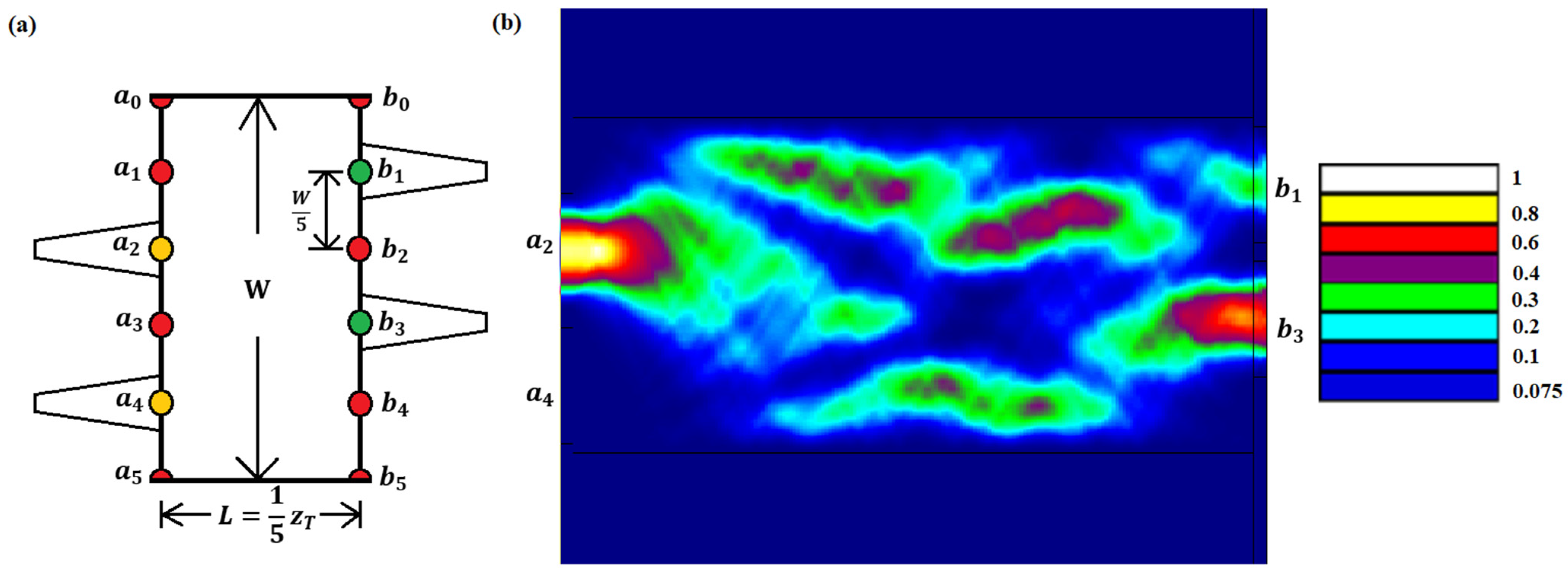
Figure 3 shows the Talbot carpets for a 3
3 MMI structure delivering the common transmission matrix
for the same physical dimensions of the waveguide.
Figure 3a depicts the complete Talbot carpet of a unit cell, consisting of the physical and virtual multimode sections. The zero field at the boundaries shows the broken translation symmetry. To observe the transmission described in Equation (18), the image plane is drawn at
and only the physical section is considered for a better perspective. A point source illuminates the multimode waveguide from lattice positions
,
, and
, as shown in
Figure 3b–d, respectively. For each case, images of the source can be observed at
and
with scaled intensity, as predicted by Equation (18). The illumination is facilitated by placing access ports at these positions, which are offset from the port position of a common 3
3 MMI coupler, where the outer access ports are positioned symmetrically about the middle. This suggests how reciprocal lateral translations of the physical port positions can lead to identical transmission characteristics in identical MMI structures. Such transmission with offset port configuration can be observed for other smaller
MMI when a larger
MMI transmission matrix is analyzed at different
-values.
2.3. Type II MMI
Type II anti-symmetry corresponds to a regular placement of
lattice points on the physical multimode waveguide’s transverse axis with no clearance to the boundaries; thus, the axis of anti-symmetry falls through a lattice point.
Figure 4 shows such a configuration. Any source at the boundary must be null. Therefore, in Type II anti-symmetry, the MMI must have no more than
physical access ports. It can be observed from
Figure 4 that:
There are 2
+ 1 lattice points, including null sources, which can be accommodated by a prolonged version of the Talbot matrix. An example of prolonged Talbot matrix with
= 3 can be expressed as:
where for
= 1,
, and thus
which confirms the automatic identification of
&
. The prolonged Talbot matrix loses its cyclic characteristics but remains symmetric and persymmetric. Therefore, Equation (11) is still valid with
and
, and hence, for the anti-symmetric part of a solution:
Removing the prolongation and using the partitioning of
:
The resultant two equations are equivalent. Either one of them can be used to determine
. For example, for
= 1,
= 3:
which is an exchange operation at a shorter interval
. For
= 2, the identity operation can be obtained at a shorter interval
.
For
= 1,
= 4:
where
. It can be observed that access port
is imaged directly onto the access port
capturing the apparent four-fold reduction in the Talbot distance due to the selective launch of a centered access waveguide. Omitting the middle access port reduces Equation (24) to the transmission matrix of a
coupler with an unequal splitting ratio, accompanied by
phase shift between ports.
Although common phase factors are provided for the examples discussed, in most applications they are irrelevant. Microfabrication is advancing, but from wafer to wafer, there will be wavelength-scale changes in path lengths; albeit, the relative path lengths of identical devices on the same wafer will be less uncertain. Since a wavelength scale change in the length of a multimode waveguide will not significantly change the magnitude and relative phase of its scattering parameters but can change its overall phase dramatically, the designer remains uncertain of the overall phase. Conservation of energy implies that is always unitary. Exchange and identity operations are inherent for any with and respectively. The anti-symmetry axis breaks the translation symmetry, and thus loses the circulant property of the Talbot matrices but retains the symmetric and persymmetric properties. For , yields a representation of a sum of a Toeplitz and Hankel matrix, which have complementary zero and non-zero entries, so the sum always has a non-zero entry from one or the other component. In contrast, for Type II, the non-zero and zero entries coincide, leading, in general, to a sparse matrix and a nonuniform split.
2.4. Golden Ratio MMI
Type II anti-symmetry imposed on a multimode waveguide with
,
leads to four physical access ports and one unusable port presented as half port at the waveguide’s boundaries. The transmission can be represented as:
where
and
. The golden ratio
is the positive root of the quadratic equation
. The negative root may be expressed as the negative reciprocal of the positive root
. By applying Ptolemy’s theorem to a regular pentagon, one obtains the identities:
Omitting ports can decompose
to an independent interlaced pair of
couplers with ideal power-splitting ratio of
without any loss:
Access ports at one side of the waveguide are offset by
relative to the other side.
Figure 5a shows the schematic of one variation in the Golden ratio MMI coupler. The FIMMPROP optical propagation tool is used to verify the design.
Figure 5b depicts the simulated field profile in the multimode section where the lattice point
is the illumination source. For other variations of
, such as
, similar transmission can be achieved:
where access ports at both sides reside at the same lattice point. For transmission matrices in Equations (28) and (29), and other cases for different values of
, the phase term
is not a part of the characteristic equation for the eigenvalues; therefore, a re-phased equivalent transmission matrix can be introduced for each case. For p = 1:
Since , focusing on is sufficient for all cases.
From Equation (30), the rows and columns of
G are orthonormal, which confirms that
G is unitary.
G is also bisymmetric, albeit the re-phasing matrices break the bisymmetry.
K is persymmetric but not symmetric. The power-splitting ratio remains the same. The eigenvalues of
are a complex conjugate pair on the unit circle:
which are approximately sixth roots of unity with the argument
.
It can be conjectured that an MMI coupler with golden power-splitting ratio is not only limited to
but also found with
an integer multiple of 5. For example, type-II anti-symmetry applied to a
= 1,
= 10 configurations can achieve a
MMI transmission matrix with golden ratio appearing in the entries after omitting the other access ports without any power loss:
3. Experimental Results and Discussion
Figure 6a depicts the microscopic image of the golden ratio MMI coupler and Mach-Zehnder delay interferometer circuit with the golden ratio MMI coupler at their ends. Device fabrication was performed on a standard Silicon-on-Insulator platform with a top Si thickness of 220 nm and buried oxide thickness of 2 μm using the multiple project wafer (MPW) run at Advanced Micro Foundry (AMF). An experimental setup, shown in
Figure 6b, is adopted for testing purposes. A tunable laser diode (Agilent 81680A, KEYSIGHT, Santa Rosa, CA, USA) with a 5 picometer wavelength resolution, has been used as the light source. A polarization controller is used to maximize fundamental TE polarization propagation, as the off-the-shelf edge coupler and the waveguide are optimized for this state. The output from the chip is captured by an optical power sensor (Agilent 81632A, KEYSIGHT, Santa Rosa, CA, USA) and analyzed by a Lightwave measurement system (Agilent 8164A, KEYSIGHT, Santa Rosa, CA, USA). The whole system is on an optical table for stabilization purposes.
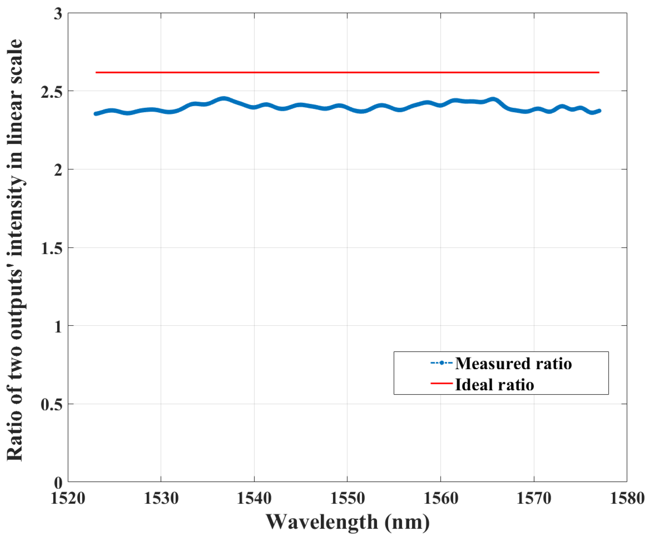
The designed golden ratio MMI coupler has a multimode waveguide section with a width of 13 μm and a length of 253.05 μm. The foundry specification for the MPW run has been maintained in the design stage, which influences the choice of minimum width. For a coupler such as this, the relative amplitude and phase among the outputs when light is launched through any input port are the most appropriate parameters for evaluation.
Figure 7 shows a comparison of the ideal and experimental ratio of light intensity exiting two output ports when one input port is connected to the tunable laser. The multimode section’s length is chosen so that the deviation of the ratio of intensity is minimized over a large wavelength range while maintaining most of the launched power in the fundamental TE mode. The experimental result shown is over a 60 nm span due to the upper limit of the wavelength of the tunable laser. Over this span of wavelength, the average measured ratio over this span has a deviation ~0.221 from the ideal ratio. Calculating the ratio removes all the fixed common loss factors and coherent fluctuations. However, the results shown here are measured with a linear scale, so any small effect can give rise to visible fluctuations. The two output measurements are performed separately; after the measurement of one output, the nanopositioning stage holding the fiber probe is adjusted for the alignment of the next output, and then another wavelength scan is taken, inevitably leading to a relatively large time delay and the possibility of alignment uncertainty, thus resulting in the deviation in the ratio. Thermal and polarization drift in laser and corresponding source power deviation can be expected for such interval. Due to aging, deterioration in the laser’s power stability, power repeatability, and power flatness over wavelength beyond the vendor specification may be another reason. The setup is not in any environment-controlled enclosure. Any low-frequency vibration of fiber probes, even from the ventilation in the laboratory, on timescales much larger than the time between two output power scans, can lead to large power fluctuations on a linear scale. Fabrication error resulting from the MPW process may be another principal cause for such deviation from the ideal ratio. To measure the relative phase, an expensive optical vector analyzer or highly sensitive interferometric architecture [
54] can be utilized. Measurement of relative phase information has not been carried out for this work.
A Mach–Zehnder delay interferometer with two golden ratio MMI couplers connected by waveguides with a path difference of 1433.967 μm, resulting in ~50 GHz free spectral range (FSR). A numerical MZDI model with an ideal golden ratio MMI coupler has been scripted in MATLAB R2020a. The resultant transmission spectrum is shown in
Figure 8a. The characteristic low extinction transmission by the interferometer’s through path is the consequence of the golden ratio MMI coupler being unbalanced. The experimental results, shown in
Figure 8b, demonstrate similar transmission characteristics. High extinction is observed at the interferometer’s cross-path transmission, whereas the through path shows low extinction.

