Article

Reconfigurable Cascaded Chirped-Grating Delay Lines for Silicon Photonic Convolutional Computing

1
School of Instrumentation Science and Opto-Electronics Engineering, Beijing Information Science and Technology University, Beijing 100192, China
2
Key Laboratory of Ministry of Education for Optoelectronic Measurement Technology and Instrument, Beijing Information Science and Technology University, Beijing 100016, China
3
School of Electronic Information, Hunan First Normal University, Changsha 410205, China
*
Author to whom correspondence should be addressed.
These authors contributed equally to this work.
Photonics 2025, 12(10), 974; https://doi.org/10.3390/photonics12100974
Submission received: 4 September 2025 / Revised: 26 September 2025 / Accepted: 26 September 2025 / Published: 30 September 2025
(This article belongs to the Section Optoelectronics and Optical Materials)

Abstract

Silicon photonic computing system is expected to replace traditional electronic computing systems in specific applications in the future, owing to its advantages in high speed, large bandwidth, low power consumption, and resistance to electro-magnetic interference. In this paper, we propose a tunable time-delay photonic computing architecture based on chirped Bragg gratings (CBG), which replaces traditional dispersion fibers to achieve the required delay function in system architecture, while providing reconfigurability capabilities of time delay control. Simulation results, using 3rd-order and 4th-order input matrices to convolve with 2nd-order convolution kernel matrices, demonstrates that the proposed photonic computing architecture can effectively perform matrix convolutional operations of various orders. Furthermore, the functionality and performance of design tunable time delay module based on CBG is also verified in the system. Therefore, our proposed scheme can be employed in the matrix multiplications of photonic computing architecture, which provides an optional efficient solution for future photonic convolutional neural networks.

1. Introduction

With the rapid development of artificial intelligence and high-speed transmission, the demands for computing and processing large volumes of data are increasingly growing. Traditional electronic computing chips are gradually approaching the limits of Moore’s Law, struggling to cope with the surge in data volume [1,2,3,4]. Against this backdrop, photonic computing, with optical signal’s large bandwidth and resistance to interference, offer a new direction for multi-channel and high-density computing technique [5]. Especially, compared with traditional electronic counterparts, photonic convolutional neural networks (CNNs) involve extensive matrix convolution operations [6,7,8], benefit significantly from photonic computing architectures, as they offer faster computing speeds and lower power consumption [9,10], while performing fundamental operations such as matrix multiplication and addition [11,12]. However, existing photonic-computing architectures—such as cascaded Mach–Zehnder interferometer arrays and micro-ring resonator structures—still face system-level reconfiguration costs when migrating across tasks or kernel sizes. In fact, on-chip tunable true-time-delay (TTD) lines have been widely demonstrated using micro-ring resonators, MZI-based switching networks, integrated Bragg-grating delays, and MEMS-assisted tuners [13,14,15,16,17,18]. The practical bottlenecks lie in fixed topologies, delay–weight interaction, footprints size and insertion loss, thermal-drift/crosstalk control, and non-trivial calibration, which collectively hinder scalability to large-scale convolutional operations [13,17,18,19,20]. Due to the challenges of current existed architectures, we propose a new photonic computing scheme based on chirped Bragg gratings (CBG), utilizing the reflection characteristics of Bragg gratings and tunable lasers to achieve dynamic adjustments of time delays, thereby optimizing the performance of photonic computing network. System simulation results have verified the feasibility of our design scheme and provided applications of this solution in convolutional operations for 2nd-order, 3rd-order, and 4th-order matrices, validating its effectiveness in achieving tunable time delay. The ability to dynamically adjust the time delay can be leveraged to optical system like photonic convolutional neural networks, optical-controlled phase arrayed antennas, and optical networks, where scalability and reconfigurability of system functionality is essential without extra hardware load. Therefore, our solution can not only address the challenges of time delay adjustment in traditional photonic computing architectures but also provide theoretical and practical support for the further development of opto-electronics hybrid systems.
Along the optical true time delay (OTTD) line of work on chirped Bragg gratings, a tunable chirped-fiber-grating prism was exploited to realize wideband TTD beamforming [21]. Configurable TTD based on cascaded chirped fiber Bragg gratings (CCFBGs) was later demonstrated for microwave-photonics links [22]. A discretely tunable delay line on-chip was realized using step-chirped subwavelength-grating (SWG) waveguide Bragg gratings [23]. Compared with these works, our silicon-on-insulator (SOI) approach—cascaded on-chip CBGs with multi-wavelength selection and fine thermal trimming—provides 0–100 ps continuous and per-channel delay reconfiguration that directly targets convolutional operations, while eliminating long dispersive fibers and reducing system-level reconfiguration overhead.
In this paper, our main work is summarized as follows. Firstly, we formulate a task-to-hardware mapping that converts target bit-shift/zero-padding rules into wavelength allocation and fine thermal trims, yielding continuous true-time-delay control (0–100 ps) with sub-ps granularity limited by laser step and calibration accuracy. Secondly, we design a reconfigurable cascaded-CBG delay unit (four stitched 10 mm bands) that maintains millimeter-scale footprint and moderate insertion loss while avoiding delay–weight interation, thereby lowering system-level reconfiguration cost compared with large MZI arrays or microcomb-dispersion networks. Thirdly, we validate the architecture via system-level simulations whose 3rd- and 4th-order inputs convolves with a 2nd-order kernel, showing consistence with the analytical model, i.e., one-to-one correspondence between mapped delays and target convolution peaks.

2. Theoretical Analysis and Mathematical Model

To overcome the lack of dynamic tunability for the traditional optical time-delay module, we propose a reconfigurable optical computing architecture utilizing chirped Bragg gratings (CBGs), which involves waveguide structures design of CBG with non-uniform periodic distributions to achieve wavelength-dependent reflective characteristics as illustrated in Figure 1. Thereby, a mapping relationship is established between wavelengths and propagation paths of optical waves. This basic principle can be expressed as
τ = 2 n e f f λ L λ c
where the τ and c represents the time-delay and light speed, respectively, and effective refractive index neff (λ) as well as reflective path L(λ) are dependent on wavelength.
Through precise modulation of grating chirp parameters, dynamic control over optical wave propagation paths for different wavelengths can be obtained, consequently constructing a dynamically reconfigurable time-delay modulation system. The period of the grating Λ(z) at some position denoted as z can be expressed as follows:
Λ z = Λ 0 + C z L 2
In above equation, Λ0 and C represents the grating period at the central position and the chirp rate of the grating, respectively, and L represents the total length of the Bragg grating. When light that satisfies the Bragg wavelength passes through the grating, it will be reflected by the grating. The central wavelength of the reflective light, denoted as λB, is called the Bragg wavelength, whose relationship with the period of the grating Λ(z) at some position is given by:
λ B = 2 n e f f λ Λ z
The calculation result of the convolutional operation for a M × M input matrix by a N × N convolutional kernel is as follows:
C m , n = i = 1 M j = 1 N w i , j A m + i 1 , n + j 1
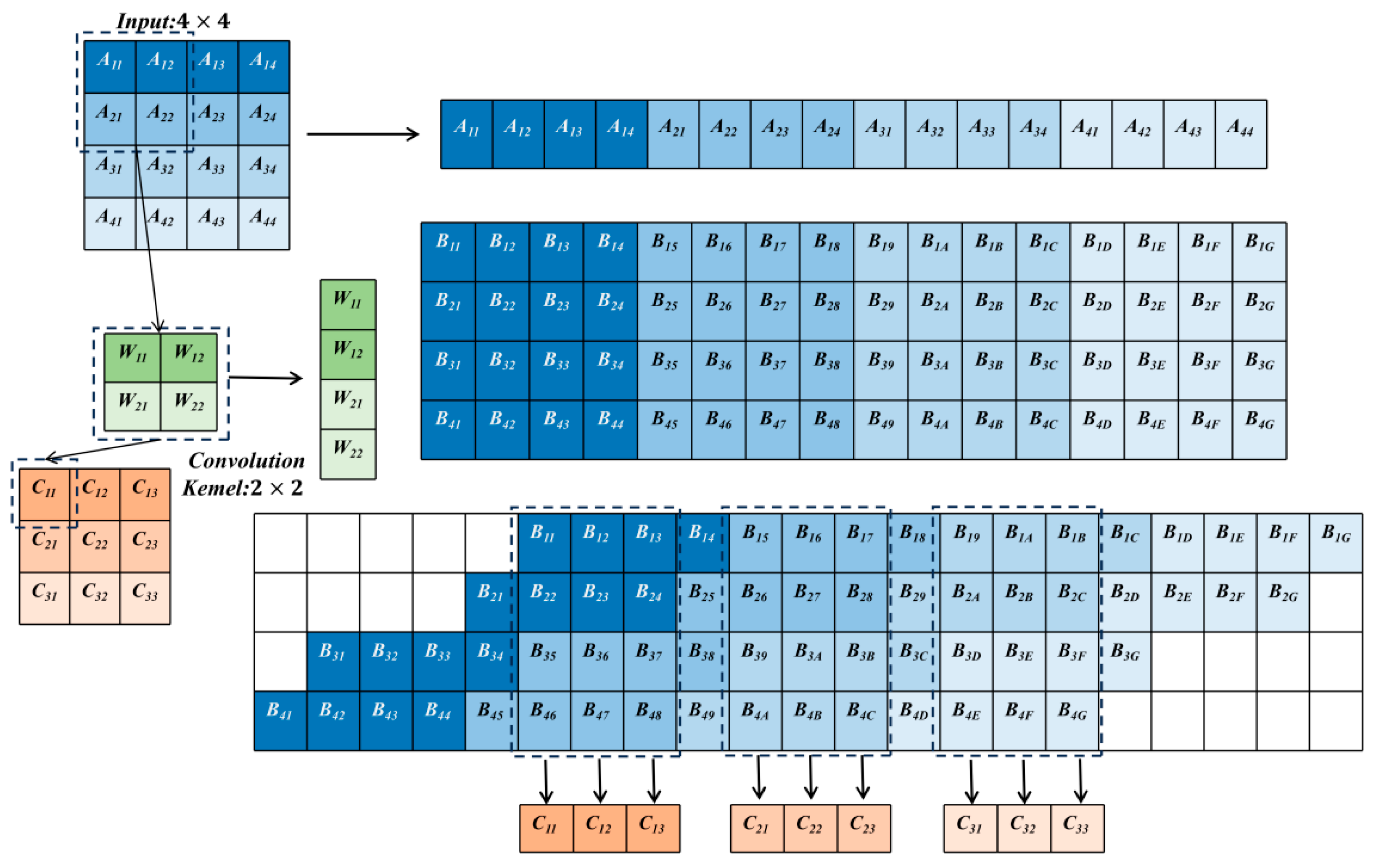
Herein, Cm,n represents the calculation result of the convolution. wi,j and Am+i−1,n+j−1 denote every element of the convolutional kernel matrix and the input matrix, respectively. As illustrated in Figure 2, in the case of M = 4 and N = 2, the specific process of performing a convolutional operation between a 4 × 4 input matrix and a 2 × 2 convolutional kernel matrix. The 4 × 4 input matrix and the 2 × 2 convolutional kernel matrix are flattened into a 1 × 16 one-dimensional row vector and a 4 × 1 one-dimensional column vector, respectively. Then these two vectors are multiplied to obtain a matrix without zero-padding, of which each row is then shifted and padded with zeros according to a specific calculation process as follows.
τ i 1 × N + j = N i × M + N j

3. Design and Implementation of On-Chip CCFBG TTD Line

3.1. Component Design

Our approach adopts a photonics computing architecture for matrix convolutional operations based on four tunable light sources and a wavelength division multiplexer. We propose a scheme on tunable time-delay using chirped Bragg gratings and tunable lasers to replace traditional optical fiber time-delay lines, thus achieving tunable time-delay. The entire photonic computing unit is composed of three parts: the signal loading module as input matrix, the convolutional kernel weight module, and the tunable time-delay module.
As shown in Figure 3, by a wavelength division multiplexer (WDM), the output optical signals of four tunable lasers are combined into a multiplexed signal that is adopted as the optical carrier of Mach-Zehnder modulator (MZM). Then, the MZM loads the data information of the input matrix onto the optical carrier. Subsequently, the optical signal carrying the information of input matrix is demultiplexed back into four separate signals by demultiplexer (DEMUX), and these four optical signals are then utilized as the input signals of four different all-pass micro-ring resonators (MRRs) carrying different weights. Remarkably, the operation process of this four MRRs essentially performs the matrix multiplication. Afterward, the four optical signals pass through a multiplexer (MUX) and a time-delay module to achieve zero-padding and addition operations. Finally, the convolutional operation between the input matrix and the convolution kernel is performed and detected by a photodetector as output. The MZM modulation signal, at the data rate of 100 Gbit/s, is with 10 ps corresponding to each delay bit. As derivation from Equation (5), If the order N of the convolution kernel is fixed while the order M of the input matrix of MZM varies, it is shown in Figure 3 that the number of zero-padding and shifting bits required for the convolutional operation changes with the order of the input matrix. The traditional approach needs to redesign and redeploy the optical delay lines to meet the requirements of new matrix operations.
Nevertheless, to flexibly address the different computational delays caused by different input matrices, this work proposes a scheme on tunable optical computing delay using chirped Bragg gratings combined with tunable lasers, which allows the same optical computing architecture to perform convolutions between input matrices and convolution kernels of different orders.
As illustrated in Figure 4, we employ four cascaded chirped Bragg gratings (CBG1–CBG4) instead of a single ultra-wideband device. Each CBG (length L = 10 mm) is written in a silica (SiO2) waveguide and designed for the fundamental TE mode with an effective refractive index neff ≈ 1.47. Each device exhibits a narrow 3-dB bandwidth of ~100 GHz. All gratings share the same length, linear chirp rate (~1% around Λ0), and raised-cosine apodization; only the central period Λ0 is offset so that CBG1–CBG4 align with the four demultiplexed WDM channels. (Bragg condition: λB ≈ 2neffΛ). The key design parameters and the group-delays are listed in Table 1.
We utilize a standard SOI platform with a 220 nm-thickness layer to fabricate the device. The CBG can be written on a 500 nm-wide silicon waveguide using a shallow-etch sidewall corrugation of ~60 nm. The grating period Λ linearly chirps from 525.6 nm to 526.6 nm along the device length, and adopts a raised-cosine apodization to suppress sidelobes and reduce group-delay ripple. To keep the design module consistent with the four WDM channels, all four cascaded CBGs have the same chirp rate and apodization, while only the central period is shifted so that each CBG aligns to single demultiplexed channel wavelength (≈1547.2, 1548.0, 1548.8, and 1549.6 nm). These four central wavelengths match the design structure in Figure 4 and process delay control per channel without redesigning the whole gratings.
Each individual CBG uses a physical length of 10 mm to accumulate sufficient group delay while maintaining a comparatively narrow and accuracy reflective bandwidth (~100 GHz). The length is distributed on chip by arranging straight segments with compact U-turns. At the same time, the overall footprint remains compatible with standard SOI and allows cascading of four CBGs as shown in Figure 4. In addition, the four CBGs preserves identical dispersion characteristics and simplifies calibration at the system level.
To obtain the fine continuously-tuned delay control, each CBG is over-cladded with SiO2 and integrated with a TiN (or polysilicon) micro-heater (typical heater area ≈ 2 µm × 300 µm) separated from the silicon waveguide by 1 µm-thickness SiO2 [24]. Leveraging thermo-optic coefficient (1.86 × 10⁻⁴ K−1) of silicon, the heater induces a Bragg-wavelength shift Δλᴮ (≥0.4 nm), which is corresponding to a continuous tuning range (0–100 ps) across the cascaded delay line by mapping relation between the wavelength and designed group-delay. The tuning preserves the narrow 3-dB bandwidth (~100 GHz) and keeps the root-mean-square ripple of the time delay below ~1 ps, while maintaining the overall insertion loss below 2.5 dB.
The identical chirp profiles and apodization of all four CBGs ensures uniform dispersion and predictable thermal responses, and only the central period offsets are adjusted to address different WDM channels. In practice, rough time-delay steps are chosen by wavelength selection (channel assignment), and fine delay is obtained by the bias of micro-heater, enabling per-channel and per-bit control without redistributing optical delay lines. This module underpins the reconfigurable time-delay parameters in Table 1.
By selectively biasing the micro-heaters on each CBG, the composite delay line delivers a continuous tuning range over 0–100 ps, a root mean square of ripple time-delay less than 1 ps, and an insertion loss lower than 2.5 dB. When the wavelength of tunable laser is selected to λ = 1547.2 nm, the signal passes through CBG1 without delay. When the light wavelengths of one channel are shifted to 1548.0 nm, 1548.8 nm, and 1549.6 nm by CBG2, CBG3, and CBG4, respectively, time-delays are correspondingly introduced as 25 ps, 50 ps and 75 ps, respectively. In addition, the heater can continuously tune the quantity of time-delay from 0 to 100 ps.
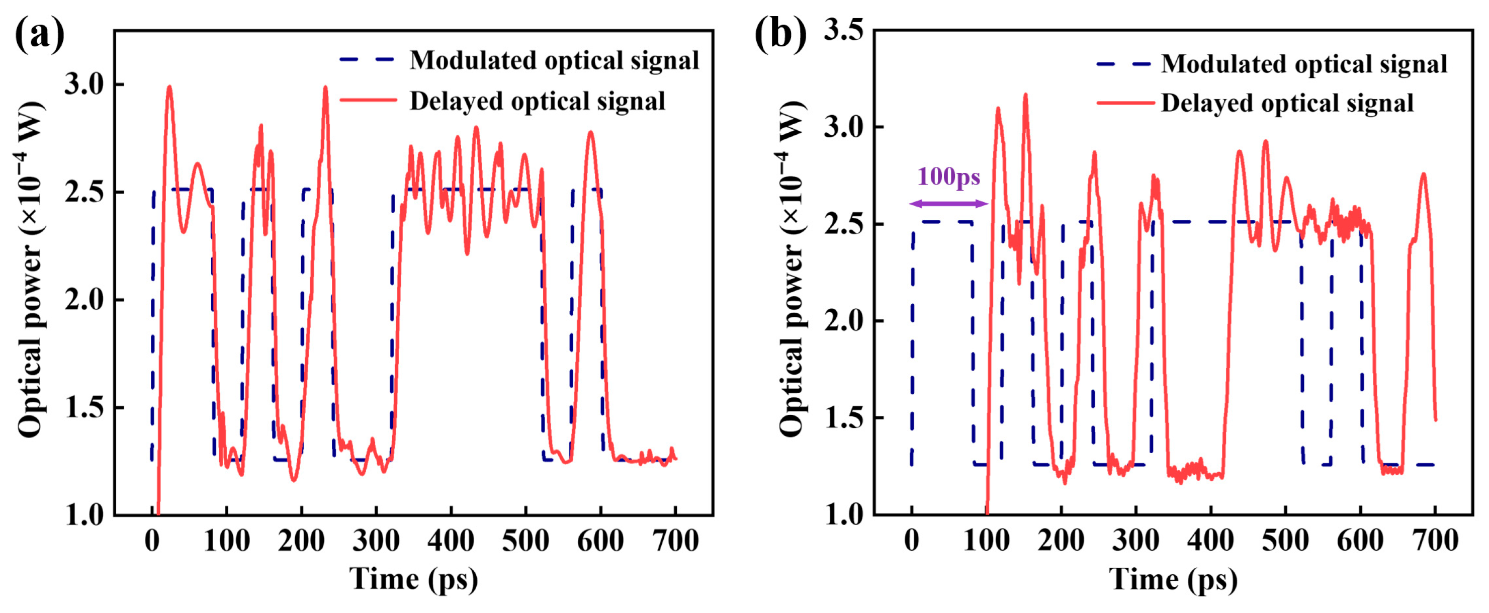
As depicted in Figure 5a, numerical simulations confirm that there is no time-delay when the wavelength of light source is selected to 1547.2 nm, while Figure 5b shows there is a cumulative time delay of 100 ps when the wavelength of light source is selected to 1550.4 nm.
For the 3rd-order matrix convolved with a 2nd-order kernel, requirements for time-delay derived from (5) are now analyzed as follows:
  • Channel 1 needs 4 bit (40 ps) → λ ≈ 1548.4 nm, time-delay: 25 ps + Δτheating (~15 ps)
  • Channel 2 needs 3 bit (30 ps) → λ ≈ 1548.0 nm, time-delay: 25 ps + Δτheating (~5 ps)
  • Channel 3 needs 1 bit (10 ps) → λ ≈ 1547.6 nm, time-delay: 0 ps +Δτheating (~10 ps)
  • Channel 4 keeps undelayed → λ = 1547.2 nm
For the 4th-order matrix convolved with a 2nd-order kernel, requirements for time-delay derived from (5) are now analyzed as follows:
  • Channel 1 needs 5 bit (50 ps) → λ ≈ 1548.8 nm, time-delay: 50 ps
  • Channel 2 needs 4 bit (40 ps) → λ ≈ 1548.4 nm, time-delay: 50 ps + Δτheating (~−10 ps)
  • Channel 3 needs 1 bit (10 ps) → λ ≈ 1547.6 nm, time-delay: 0 ps + Δτheating (~10 ps)
  • Channel 4 keeps undelayed → λ = 1547.2 nm

3.2. On-Chip Implementation and Manufacturability

We consider two complementary implementations approaches those target comparison between rapid prototyping with large delays and highly integrated operation with low reconfiguration. A CFBG can be grating-coupled to a silicon photonic die to deliver optical true time delay from hundreds of picoseconds up to the several nanoseconds without altering the on-chip structure. This option enables fast system-level validation and parameter exploration, at the cost of packaging complexity, high coupling loss, weak thermal stabilization, and chip size. Moreover, linear chirp and apodization are designed on SOI via sidewall corrugation (period/duty-cycle or etch-depth modulation), and micro-heaters that is placed on top of the grating can provide fine thermal tuning and post-fabrication trimming. To obtain the path length required for 100 ps delays, we employ a folded, U-turns serpentine layout so that a 10 mm length physical CBG is within a millimeter-scale footprint (sub-mm2 area), which fits the SOI chip size with appropriate bend radii. Notably, thermal isolation trenches to limit bending loss and cross-talk. In addition, This flow relies on standard SOI platform, enabling seamless co-integration with MRRs, modulators, and photodiodes.

3.3. Comparison of Delay Schemes and Positioning of This Work

To make the trade-offs between architecture and implementation, Table 2 shows the comparison among MZI arrays (phase/interferometric), microcomb-based dispersive TTD/WDM networks, fixed-fiber-delay PCNN, and our proposed cascaded CBG (true time delay) along the axes of delay range/step, reconfigurability, insertion loss and footprint, as well as power/calibration complexity [25,26,27,28,29,30]. The comparison indicates that, under the same footprint and packaging constraints, the cascaded CBG provides a 0–100 ps continuously tunable true time delay via wavelength selection plus low-power thermal trimming, with sub-picosecond granularity determined by laser step and calibration accuracy, while maintaining a millimeter-scale footprint and moderate loss/calibration cost. This enables reuse of the same hardware topology across different convolution orders with significantly reduced reconfiguration cost compared with other schemes.

4. Numerical Simulation and Results Analysis

4.1. Computing Results of 3rd-Order Matrix Convolution

To perform matrix convolutional operation, a 3rd-order input matrix is denoted as
1 1 0 0 0 1 0 1 1
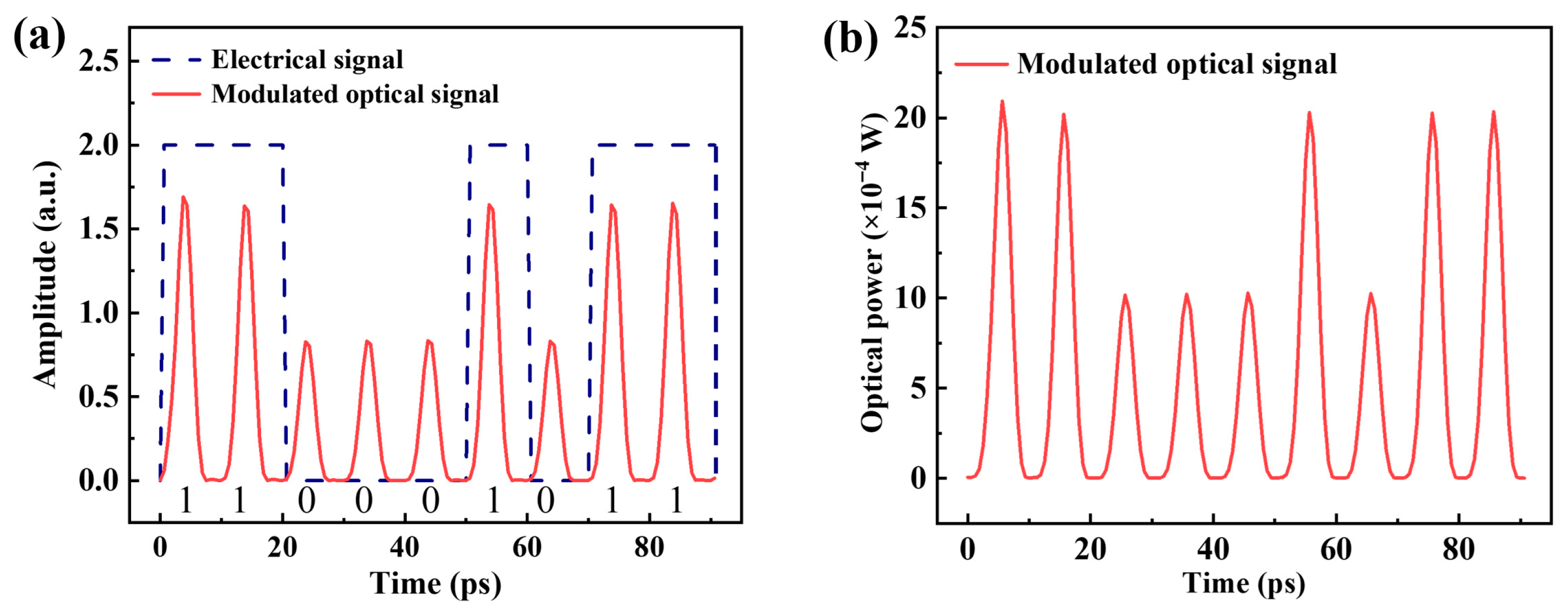
which is converted into a one-dimensional vector that is represented as [1 1 0, 0 0 1, 0 1 1]. As illustrated in Figure 6a, this information is then encoded on the optical waves in the form of electrical signals via an MZM. As depicted in Figure 6a, the blue dash-line and red line indicate the electrical signals and the modulated optical signals, respectively, which both represent data.
As illustrated in Figure 6b, the modulated optical signals pass through an erbium-doped fiber amplifier (EDFA) and a wavelength division multiplexer (WDM), where signals representing ‘1’ are amplified to 20, and those representing ‘0’ are amplified to 10. Consequently, the numerical representation of the input matrix [1 1 0, 0 0 1, 0 1 1] is transformed into matrix [20 20 10, 10 10 20, 10 20 20].
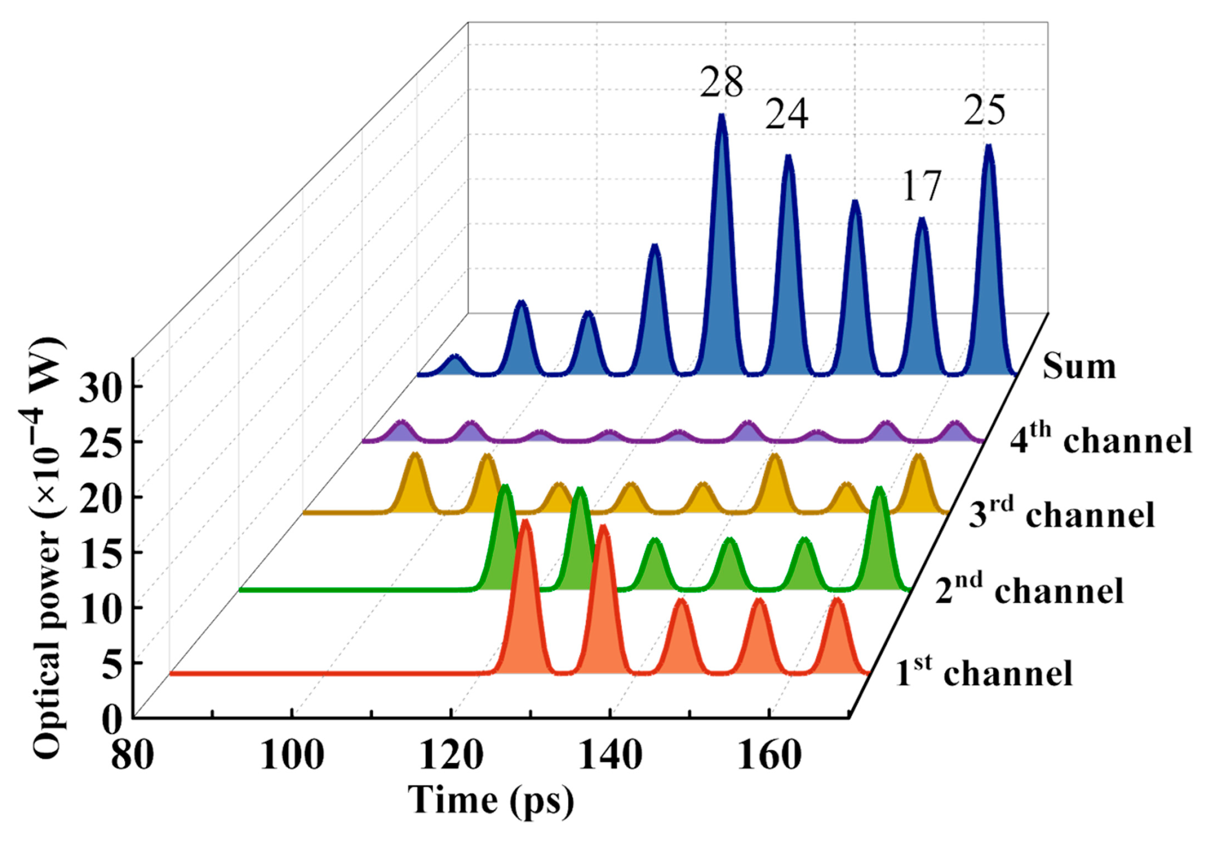
Obviously, the weights of the four MRRs can be configured in the numerical simulation. As depicted in Figure 7, the output optical signal from 1st channel to 4th channel passes through a micro-ring resonator with a weight of 0.7, 0.5, 0.3, 0.1, respectively. As shown in Figure 7, the amplitudes of the optical waves from 1st channel to 4th channel falls following the decrease of the weights from MRR1 to MRR4. In addition, due to the increase in wavelength from 4th channel to 1st channel, the time-delay of the optical waves increases sequentially. The bule waveform represents the aggregated result of the amplitudes of all the four channels. Therefore, it can be observed that the fifth, sixth, eighth, and ninth wave peaks of the summation waveform precisely match the results of the convolutional operation in Equation (4).

4.2. Computing Results of the 4th-Order Matrix Convolution

Assume a fourth-order input matrix is represented as
1 1 1 1 1 1 0 1 1 0 1 1 1 0 0 1
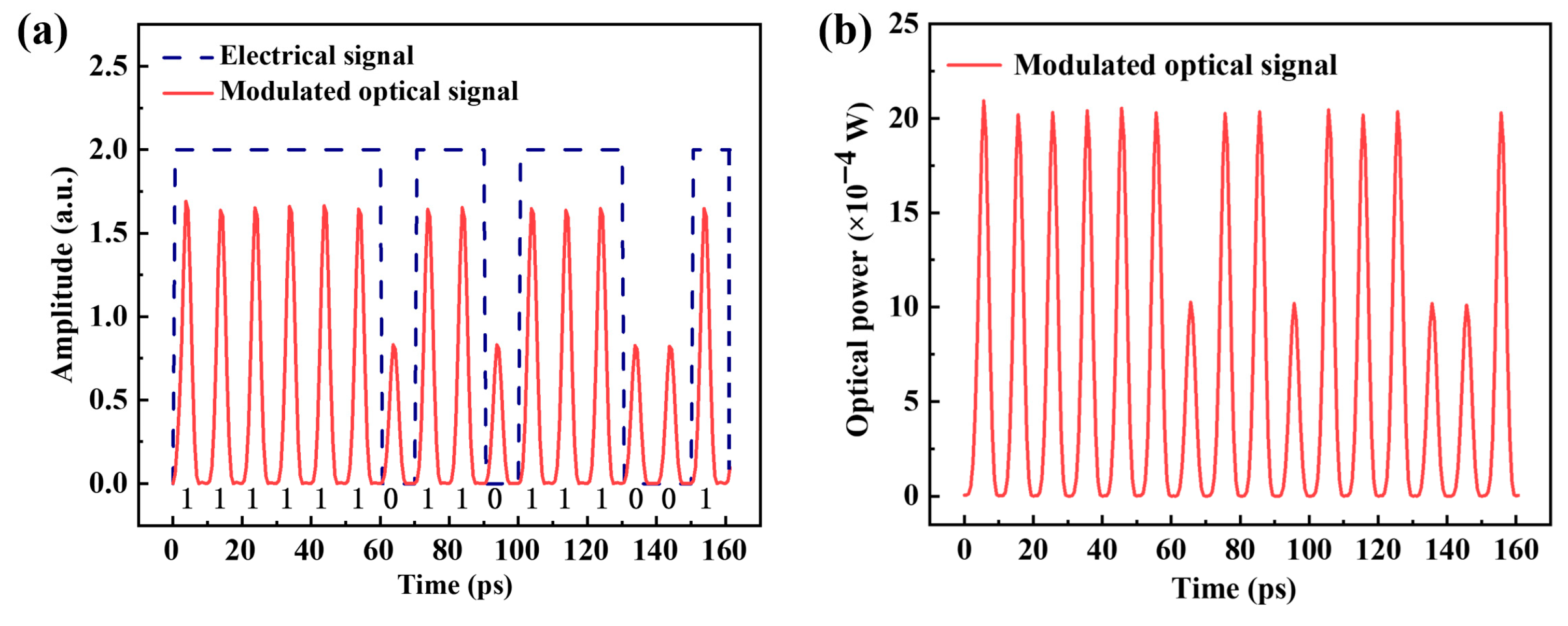
it is then converted into a one-dimensional vector that is denoted as [1 1 1 1, 1 1 0 1, 1 0 1 1, 1 0 0 1]. As illustrated in Figure 8a, this information is subsequently encoded into optical waves in the form of electrical signals via an MZM. As depicted in Figure 8a, blue dash-line signifies the electrical signals that represents data, while red line indicates the modulated optical signals.
As depicted in Figure 8b, the modulated optical signals are amplified by an EDFA and then pass through a WDM. After above amplification, values representing ‘1’ are amplified to 20, and those representing ‘0’ are amplified to 10.
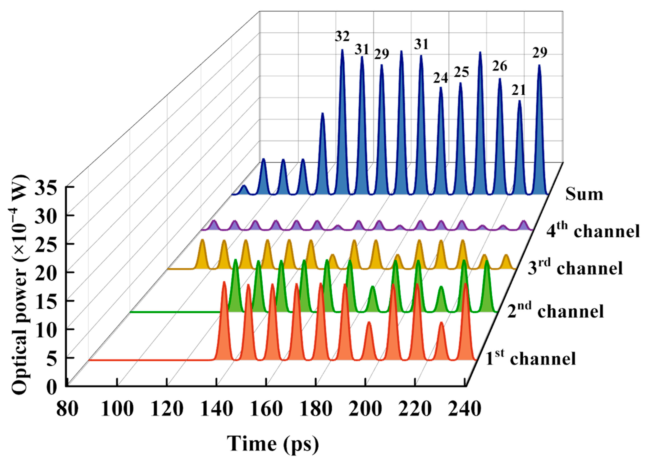
Thus, the numerical representation of the input matrix is denoted as matrix [20 20 20 20, 20 20 10 20, 20 10 20 20, 20 10 10 20]. Assuming the convolution kernel is [0.7 0.5, 0.3 0.1], the computational results of the convolution are expected to be [32 31 29, 31 24 25, 26 21 29].
Obviously, the weights of the four MRRs can be configured in the numerical simulation. As depicted in Figure 9, the output optical signal from 1st channel to 4th channel passes through a micro-ring resonator with a weight of 0.7, 0.5, 0.3, 0.1, respectively. As shown in Figure 9, the amplitudes of the optical waves from 1st channel to 4th channel falls following the decrease of the weights from MRR1 to MRR4. In addition, due to the increase in wavelength from 4th channel to 1st channel, the time-delay of the optical waves increases sequentially. The bule waveform represents the aggregated result of the amplitudes of all the four channels. Therefore, it can be observed that the sixth, seventh, eighth, tenth, eleventh, twelfth, fourteenth, fifteenth, and sixteenth wave peaks of the summation waveform precisely match the results of the convolutional operation in Equation (4).

4.3. Group-Delay and Reflection Characteristics of the Cascaded CBG Delay Line

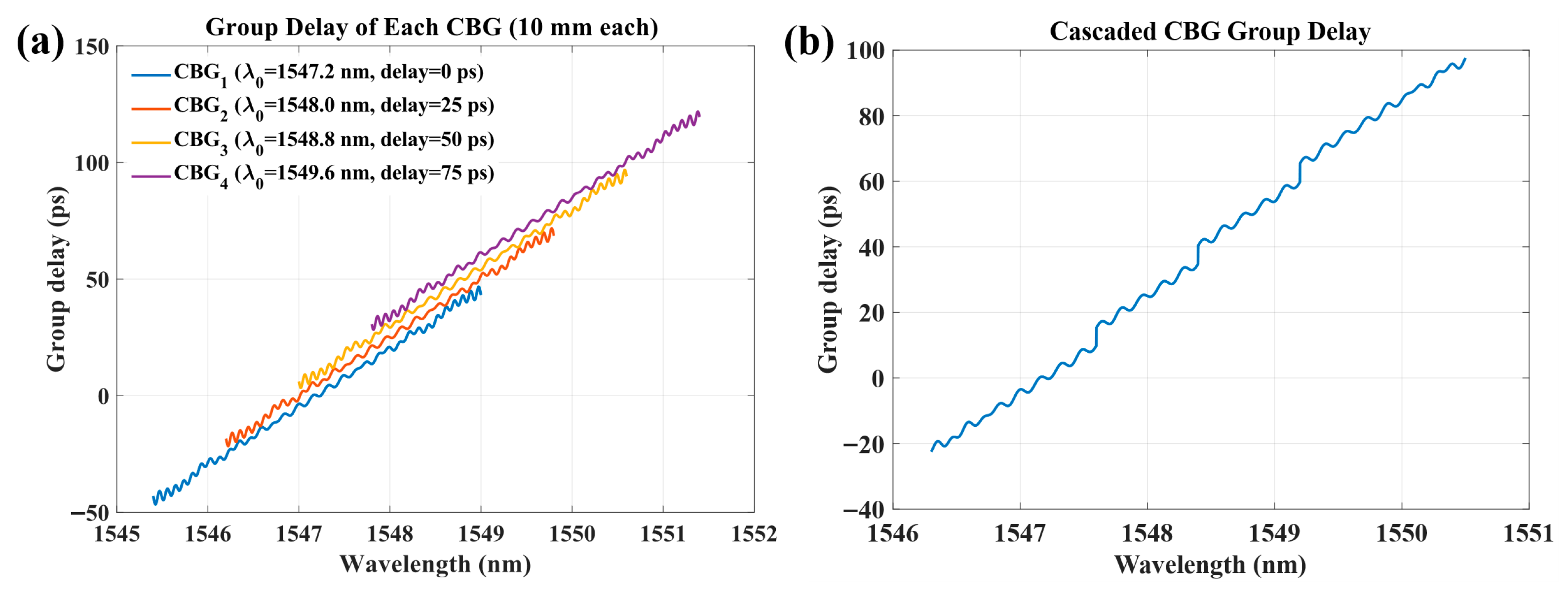
To validate the spectral–temporal consistency of the cascaded CBG delay module, we use a CMT/TMM model to numerically simulate the four CBGs listed in Table 1 with operation central wavelengths of 1547.2, 1548.0, 1548.8, and 1549.6 nm, respectively and each CBG length of 10 mm. The final group-delay results of the four CBGs along the central wavelength are illustrated in Figure 10. As shown in Figure 10a, the group delay of each CBG increases linearly with the change in wavelength with an approximate slope of ~25 ps/nm, and the initial group delay of the four CBGs are sequentially offset by 0, 25, 50, and 75 ps, respectively, maintaining the superimposed group-delay ripple (GDR) within 2–3 ps. As illustrated in Figure 10b, the cascaded CBG group delay provides a continuously tunable true-time delay from 0 to 100 ps with central wavelength spanning from 1546.2 to 1550.4 nm. Small steps at band transitions originate from sub-band stitching and can be removed by per-section micro-heater trimming (±12 ps) shown in Table 1.
Figure 11a presents the reflective spectra of individual CBG, showing a near-flat-top response with a typical in-band reflectivity of −12 ± 0.5 dB and a 3-dB bandwidth spanning over 0.8–1.0 nm. Furthermore, as illustrated in Figure 11b, the cascaded CBG reflective spectrum remains from −12 to −13 dB across the stitched band with narrow dips (<1 dB) around the hand-over wavelengths. These results indicate that, while satisfying the zero-padding and alignment requirements of different convolutional orders and maintaining in-band reflectivity and delay linearity appropriate for system mapping and calibration, the cascaded CBG delay line offers continuous and fine-granularity OTTD control via wavelength selection plus low-power thermal trimming without altering the hardware topology.

5. Conclusions

A photonic computing architecture for matrix convolutional operations is designed and verified based on chirped Bragg gratings utilized as time-delay module that can perform continuously tunable time-delay from 0 to 100 ps. By dynamically adjusting the time-delay, this system can perform convolutional operations on input matrices of different orders using mere a fixed hardware setup, thus providing the entire system with reconfigurability. This architecture successfully demonstrates the feasibility of adjustable convolutional operations using tunable time-delay module—chirped Bragg gratings combined with tunable lasers—to input 3rd-order and 4th-order matrices with a 2nd-order convolutional kernel. Although the implementation of photonic convolutional neural network (PCNN) faces the challenge of dynamic resource allocation, our proposed scheme could achieve less hardware overload and more flexible resource allocation due to dynamic configurability of the convolutional computing unit using tunable time-delay module. Therefore, this design architecture processes broad potentials in the application of PCNN acceleration computing in future.

Author Contributions

Conceptualization, G.Z. and G.C.; methodology, G.Z., L.L. and Y.X.; software, G.Z. and F.S.; validation, G.Z., F.S. and G.C.; formal analysis, G.Z., G.C. and L.L.; investigation, G.Z., S.C. and Y.L.; resources, G.C. and L.L.; data curation, G.Z. and B.W.; writing—original draft preparation, G.Z.; writing—review and editing, G.Z. and G.C.; visualization, G.Z., J.Y. and G.C.; supervision, G.C. and L.L.; project administration, G.C.; funding acquisition, G.C. and L.L. All authors have read and agreed to the published version of the manuscript.

Funding

This work is supported by National Natural Scientific Fund of China (No. 62205029), Scientific Research Plan Project of Beijing Municipal Education Commission (No. KM202411232020), Young Backbone Teacher Support Plan (No. YBT202408), Scientific Research Foundation of Beijing Information Science and Technology University (No. 2023XJJ08).

Institutional Review Board Statement

Not applicable.

Informed Consent Statement

Not applicable.

Data Availability Statement

Data are contained within the article.

Conflicts of Interest

The authors declare no conflicts of interest.

References

  1. Chen, H.; Yu, Z.; Zhang, T.; Zang, Y.; Dan, Y.; Xu, K. Advances and challenges of optical neural networks. Chin. J. Lasers 2020, 47, 0500004. [Google Scholar] [CrossRef]
  2. Fu, T.; Sun, R.; Huang, Y.; Zhang, J.; Yang, S.; Zhu, Z.; Chen, H. Review of on-chip integrated optical neural networks. Chin. J. Lasers 2024, 51, 0119002. [Google Scholar] [CrossRef]
  3. Huang, Y.; Zhang, W.; Yang, F.; Du, J.; He, Z. Programmable matrix operation with reconfigurable time-wavelength plane manipulation and dispersed time delay. Opt. Express 2019, 27, 20456–20467. [Google Scholar] [CrossRef]
  4. Bortnik, B.; Hung, Y.-C.; Tazawa, H.; Seo, B.-J.; Luo, J.; Jen, A.K.-Y. Electrooptic polymer ring resonator modulation up to 165 GHz. IEEE J. Sel. Top. Quantum Electron. 2007, 13, 104–110. [Google Scholar] [CrossRef]
  5. Jiang, Y.; Zhang, W.; Yang, F.; He, Z. Photonic Convolution Neural Network Based on Interleaved Time-Wavelength Modulation. J. Light. Technol. 2021, 39, 4592–4600. [Google Scholar] [CrossRef]
  6. Jiang, Z.; Huang, C.-B.; Leaird, D.E.; Weiner, A.M. Optical arbitrary waveform processing of more than 100 spectral comb lines. Nat. Photonics 2007, 1, 463–467. [Google Scholar] [CrossRef]
  7. Shu, C.; Xie, Q. Programmable schemes on temporal processing of optical pulses for high-speed photonic subsystems. In Optical Fiber Communication Conference (OFC); Optical Society of America: Washington, DC, USA, 2019; p. M1B.1. [Google Scholar] [CrossRef]
  8. Touch, J.; Badawy, A.; Sorger, V. Optical computing. Nanophotonics 2017, 6, 503–505. [Google Scholar] [CrossRef]
  9. Brunner, D.; Soriano, M.C.; Fischer, I. High-speed optical vector and matrix operations using a semiconductor laser. IEEE Photonics Technol. Lett. 2013, 25, 1680–1683. [Google Scholar] [CrossRef]
  10. Huang, Y.; Zhang, W.; Yang, F.; He, Z. Optical matrix manipulation based on frequency comb modulation and dispersed time delay. In Optical Fiber Communication Conference (OFC); Optical Society of America: Washington, DC, USA, 2019; p. M1B.4. [Google Scholar] [CrossRef]
  11. Lin, J.; Sepehrian, H.; Xu, Y.; Rusch, L.A.; Shi, W. Frequency comb generation using a CMOS compatible SiP M-MZM for flexible networks. IEEE Photonics Technol. Lett. 2018, 30, 1495–1498. [Google Scholar] [CrossRef]
  12. Li, Y.; Li, J.; Huo, Y.; Chen, M.; Yang, S.; Chen, H. Spatial-mode-coupling-based dispersion engineering for integrated optical waveguide. Opt. Express 2018, 26, 2807–2816. [Google Scholar] [CrossRef] [PubMed]
  13. Shi, S.; Niu, H.; Shi, W.; Lin, D.; Li, S.; Pan, S.; Yun, B. Integrated Optical Tunable Delay Line and Microwave Photonic Beamforming Chip: A Review. Laser Photonics Rev. 2025, 19, 2400663. [Google Scholar] [CrossRef]
  14. Cardenas, J.; Foster, M.A.; Sherwood-Droz, N.; Poitras, C.B.; Lira, H.L.R.; Zhang, B.; Gaeta, A.L.; Khurgin, J.B.; Morton, P.; Lipson, M. Wide-bandwidth continuously tunable optical delay line using silicon microring resonators. Opt. Express 2010, 18, 26525–26534. [Google Scholar] [CrossRef]
  15. Xiang, C.; Davenport, M.L.; Khurgin, J.B.; Morton, P.A.; Bowers, J.E. Low-Loss Continuously Tunable Optical True Time Delay Based on Si3N4 Ring Resonators. IEEE J. Sel. Top. Quantum Electron. 2018, 24, 5900109. [Google Scholar] [CrossRef]
  16. Xie, J.; Zhou, L.; Li, Z.; Wang, J.; Chen, J. Seven-bit reconfigurable optical true time delay line based on silicon integration. Opt. Express 2014, 22, 22707–22715. [Google Scholar] [CrossRef] [PubMed]
  17. Li, Y.; Xu, L.; Wang, D.; Huang, Q.; Zhang, C.; Zhang, X. Large group delay and low loss optical delay line based on chirped waveguide Bragg gratings. Opt. Express 2023, 31, 4630–4638. [Google Scholar] [CrossRef] [PubMed]
  18. Liao, K.; Li, C.; Dai, T.; Zhong, C.; Lin, H.; Hu, X.; Gong, Q. Matrix eigenvalue solver based on reconfigurable photonic neural network. Nanophotonics 2022, 11, 4089–4099. [Google Scholar] [CrossRef]
  19. Song, Q.Q.; Hu, Z.F.; Chen, K.X. Scalable and reconfigurable true time delay line based on an ultra-low-loss silica waveguide. Appl. Opt. 2018, 57, 4434–4439. [Google Scholar] [CrossRef]
  20. Hong, M.S.; Lim, M.G.; Kim, D.U.; Her, M.J.; Park, Y.J.; Choi, D.J.; Jeong, Y.; Park, J.; Han, S.; Chun, Y.H.; et al. Programmable MZI based on a silicon photonic MEMS-tunable delay line. Opt. Lett. 2023, 48, 5611–5614. [Google Scholar] [CrossRef] [PubMed]
  21. Liu, Y.; Yao, J.; Yang, J. Wideband true-time-delay beam former that employs a tunable chirped fiber grating prism. Appl. Opt. 2003, 42, 2273–2277. [Google Scholar] [CrossRef]
  22. Zhao, J.; Ding, Z.; Yang, F.; Cai, H. Configurable photonic true-time delay line based on cascaded linearly chirped fiber Bragg grating. In Proceedings of the 2018 International Topical Meeting on Microwave Photonics (MWP), Toulouse, France, 22–25 October 2018; pp. 1–4. [Google Scholar] [CrossRef]
  23. Sun, H.; Wang, Y.; Chen, L.R. Integrated discretely tunable optical delay line based on step-chirped subwavelength grating waveguide Bragg gratings. J. Light. Technol. 2020, 38, 5551–5560. [Google Scholar] [CrossRef]
  24. Saccomandi, P.; Varalda, A.; Gassino, R.; Tosi, D.; Massaroni, C.; Caponero, M.A.; Pop, R.; Korganbayev, S.; Perrone, G.; Diana, M.; et al. Linearly chirped fiber Bragg grating response to thermal gradient: From bench tests to the real-time assessment during in vivo laser ablations of biological tissue. J. Biomed. Opt. 2017, 22, 097002. [Google Scholar] [CrossRef]
  25. Hunter, D.B.; Parker, M.E.; Dexter, J.L. Demonstration of a Continuously Variable True-Time Delay Beamformer Using a Multichannel Chirped Fiber Grating. IEEE Microw. Theory Tech. 2006, 54, 861–867. [Google Scholar] [CrossRef]
  26. Alam, M.S.; Li, X.; Jacques, M.; Berikaa, E.; Koh, P.C.; Plant, D.V. Net 300 Gbps/λ transmission over 2 km of SMF with a silicon photonic mach-zehnder modulator. IEEE Photonics Technol. Lett. 2021, 33, 1391–1394. [Google Scholar] [CrossRef]
  27. Cui, K.; Rao, S.; Xu, S.; Huang, Y.; Cai, X.; Huang, Z.; Wang, Y.; Feng, X.; Liu, F.; Zhang, W.; et al. Spectral convolutional neural network chip for in-sensor edge computing of incoherent natural light. Nat. Commun. 2025, 16, 81. [Google Scholar] [CrossRef]
  28. Zou, Z.; Zhou, L.; Wang, M.; Wu, K.; Chen, J. Tunable spiral Bragg gratings in 60-nm-thick silicon-on-insulator strip waveguides. Opt. Express 2016, 24, 12831–12839. [Google Scholar] [CrossRef] [PubMed]
  29. Chen, Z.; Flueckiger, J.; Wang, X.; Zhang, F.; Yun, H.; Lu, Z.; Caverley, M.; Wang, Y.; Jaeger, N.A.F.; Chrostowski, L. Spiral Bragg grating waveguides for TM mode silicon photonics. Opt. Express 2015, 23, 25295–25307. [Google Scholar] [CrossRef]
  30. Hong, S.; Zhang, L.; Wang, Y.; Zhang, M.; Xie, Y.; Dai, D. Ultralow-loss compact silicon photonic waveguide spirals and delay lines. Photonics Res. 2022, 10, 1–7. [Google Scholar] [CrossRef]
Figure 1. (a) Operation principles of a fiber Bragg grating: left blue arrow-incident spectrum; red arrow-reflected spectrum; right blue arrow-transmitted spectrum. (b) Schematic diagram of tunable time-delay mechanism for CFBG: black curved arrows-position-dependent Bragg reflections at different locations along the chirped grating; red curved arrow-reflection at the left end (smaller grating period) corresponding to the shorter wavelength λshort; blue curved arrow-reflection at the right end (larger grating period) corresponding to the longer wavelength λlong. FBG: fiber Bragg grating. CFBG: chirped fiber Bragg grating.
Photonics 12 00974 g001
Figure 2. Process of convolutional operations and zero-padding using chirped Bragg grating. Color coding: blue tiles denote the input matrix A (and its serialized/zero-padded sub-blocks B during the sliding-window step); green tiles denote the 2 × 2 convolution kernel W; orange tiles denote the output matrix C. The shade of the blue tiles encodes the row index (darker = upper rows, lighter = lower rows), serving only to visually trace row-wise ordering during serialization and window shifts.
Photonics 12 00974 g002
Figure 3. Schematic diagram of photonic neural network using CBG time-delay module. Color/trace legend: the blue square-wave at the far left denotes the electrical drive applied to the modulator; the red waveform denotes the resulting optical signal after modulation. At the output of the delay module, the four pulse trains in cyan, yellow, orange, and red represent four wavelength (or channel) paths, each experiencing a different group delay. The light-blue trace indicates the photodetected, weighted-sum waveform—i.e., the final computational result.
Photonics 12 00974 g003
Figure 4. Cascaded chirped Bragg gratings. Color coding: within each CBG, the dark-to-light blue gradient encodes the linear chirp of the local grating period Λ(z).
Photonics 12 00974 g004
Figure 5. (a) Time-delay generated by light at 1547.2 nm passing through the chirped grating. (b) Time-delay generated by light at 1550.4 nm passing through the chirped grating.
Photonics 12 00974 g005
Figure 6. (a) Modulation results of the 3rd order matrix. (b) Amplified optical signals.
Photonics 12 00974 g006
Figure 7. Convolutional results of 3rd order matrix and 2nd order convolution kernel.
Photonics 12 00974 g007
Figure 8. (a) Modulation results of the 4th order matrix. (b) Amplified optical signals.
Photonics 12 00974 g008
Figure 9. Convolutional results of 4th order matrix and 2nd-order convolution kernel.
Photonics 12 00974 g009
Figure 10. (a) Group-delay of the four 10-mm CBGs. (b) Composite group-delay.
Photonics 12 00974 g010
Figure 11. (a) Reflection spectra of the four CBGs. (b) Composite reflection spectrum.
Photonics 12 00974 g011
Table 1. Design parameters and tunable range of the four cascaded chirped Bragg gratings.
GratingCentral Wavelength λ (nm)Period of the CBG Λ (nm)Design Group Delay (ps)Fine-Tuning by Heating (ps)
CBG11547.2525.60±12
CBG21548.0525.925±12
CBG31548.8526.350±12
CBG41549.6526.675±12
Table 2. Summary on the comparisons among time-delay schemes for photonic computing.
SchemeDelay Range/StepReconfigurabilityInsertion LossFootprintPower/Calibration Complexity
MZI arrays (phase)0–100 ps; step 1–5 psHigh (continuous weights, discrete paths)10–20 dB (scale-dependent)>a few mm2 (O(N2) ports)0.5–2 W; complex (multi-parameter non-convex tuning)
Microcomb + dispersive network (TTD/WDM)0.1→1000 psMedium (selectable channels/weights, but discrete)15–30 dB (WDM/EOM/EDFA accumulation)often cm-scale dispersion/peripherals\
Fixed-fiber-delay PCNN (discrete branches)Discrete by fiber length (10 ps-ns)Medium (switch/selection only)<5 dB per branch (excluding couplers)coiled fiber/rack-scale\
Our design cascaded CBG (true time delay)0–100 ps continuous (in-band); step < 1 psHigh (continuous true delay; reusable across convolution orders)≈1–3 dB per grating; cascade ≈4–8 dB (process-dependent)<10 mm × few hundred μm<100 mW (steady-state thermal)
Disclaimer/Publisher’s Note: The statements, opinions and data contained in all publications are solely those of the individual author(s) and contributor(s) and not of MDPI and/or the editor(s). MDPI and/or the editor(s) disclaim responsibility for any injury to people or property resulting from any ideas, methods, instructions or products referred to in the content.