Abstract
Buttcoupling is the most efficient way to excite surface plasmon polariton (SPP) waves at dielectric/metal interfaces in order to realize applications in broadband and ultra-compact integrated circuits (IOCs). We propose a reasonable waveguide structure to efficiently excite and collect the SPP waves supported in a plasmonic trench waveguide in the long-haul telecommunication wavelength range. Our simulation results show that the coupling efficiency between the dielectric strip waveguides and a plasmonic trench waveguide can be optimized, which is dominated by the zigzag propagation path length in the dielectric strip loaded on the metal substrate. It is noted that nearly a 100% coupling efficiency can be achieved when the distance between the excitation source and the plasmonic waveguide is about 6.76 μm.
1. Introduction
At dielectric/metal interfaces, the electromagnetic (EM) waves can be bounded and thereby form surface plasmon polariton (SPP) waves when the operating frequency is lower than the plasma frequency of the metal [1]. During the propagation of SPP waves, the electrons in the top region of the metal collectively interact with the EM waves, which forms two exponential decay waveforms. The light waves are localized near the dielectric/metal interfaces and thereby allow for a smaller bending radius in the waveguide structures [2]. Various sub-wavelength plasmonic-waveguide-based components have been designed and/or proposed in order to realize broadband and ultra-compact integrated optical circuits (IOCs), such as polarization beam splitters [3,4], super prisms [5,6], Mach–Zehnder interferometers [7,8], and band pass filters [9,10]. However, the intrinsic ohmic loss of metals hinders developments in plasmonic-waveguide-based OICs.
Previously, various metallic waveguide structures were proposed to increase the propagation distance while keeping sub-wavelength modal sizes, such as V-groove, wedge, and trench-based plasmonic waveguides [11,12,13,14]. When the lateral size of the plasmonic waveguides is smaller than 200 nm, the propagation length is about 100 μm in the long-haul telecommunication wavelength range. According to the wave-interference mechanisms, two or three plasmonic components can be integrated within a propagation length of 100 μm. Therefore, it is necessary to connect plasmonic components with low-loss dielectric waveguides [15] and to increase the optical signals with dielectric-waveguide-based amplifier devices [16]. The optical coupling efficiency between a dielectric waveguide and a plasmonic waveguide has been numerically investigated in order to minimize the insertion loss owing to the modal-field and modal-index mismatches [17,18]. However, these proposed efficient couplers are not easy to use in low-loss plasmonic waveguides, which limits the development of plasmonic-based OICs.
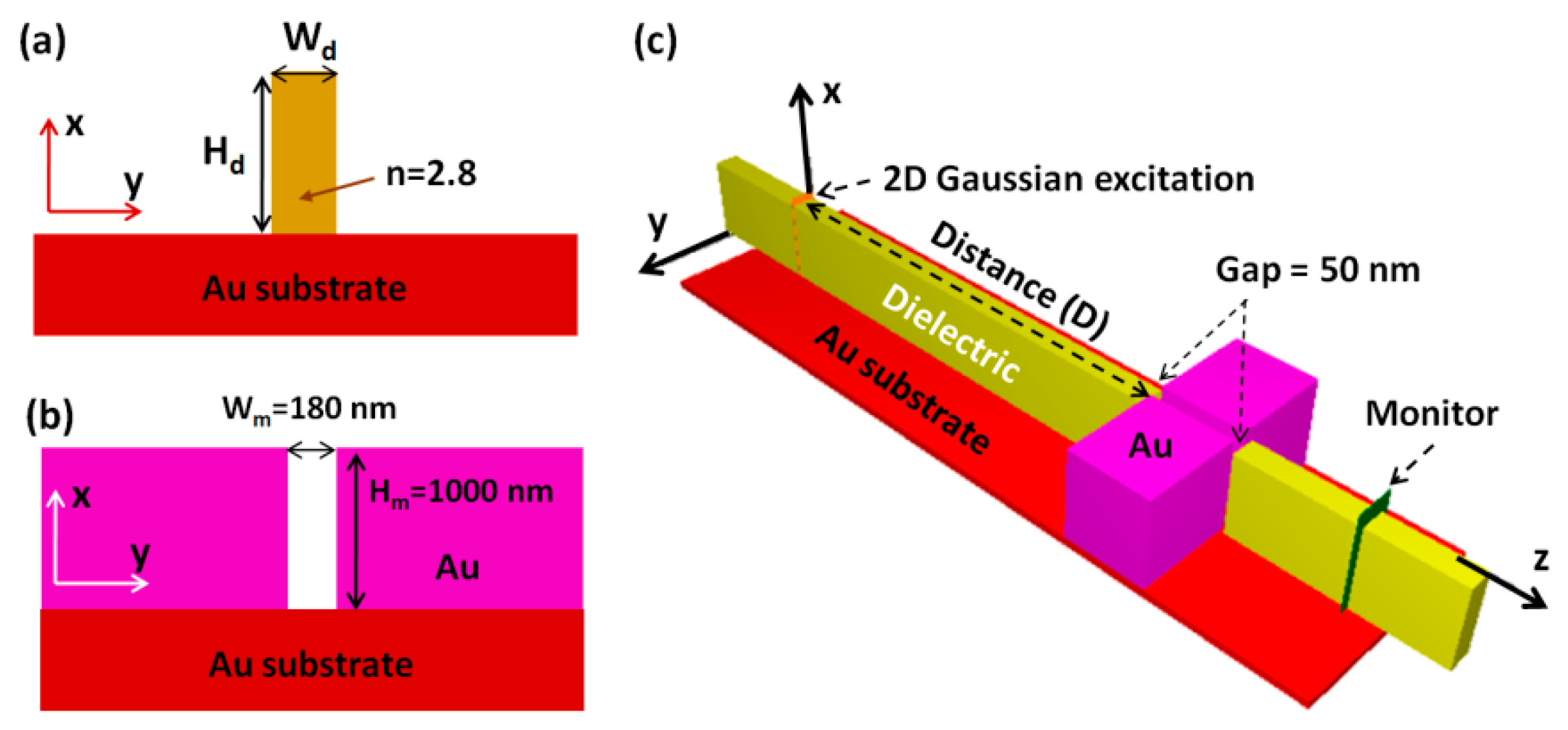
Among these low-loss sub-wavelength plasmonic waveguides, the plasmonic trench waveguides have a relatively long propagation length in the long-haul telecommunication wavelength range. Therefore, it is worthwhile investigating the coupling efficiency between the input (output) dielectric waveguide and the plasmonic trench waveguide. To consider the fabrication of the input and output couplers, the two dielectric strips are partially loaded on the metal substrate in order to excite and collect the SPP waves supported in the plasmonic trench waveguide via the buttcoupling method [19,20], as shown in Figure 1. The fabrication methods are illustrated in Figure S1, which contain lithography, dry etching, thermal evaporation, oxidation, and sputter processes. The electron-beam lithography method allows for the fabrication of nano-scaled structures in the lateral directions. The spatial resolution of e-beam lithography is about 2 nm [21]. The dry etching, thermal evaporation, oxidation, and sputter methods allow for the fabrication of nano-scaled structure in the vertical direction. The etching, deposition, and oxidation rates can be precisely controlled at about 0.1 nm/s, which results in accurate fabrications in terms of depth, thickness, and height [22,23,24,25]. In addition, the proposed fabrication methods have been used to fabricate photonic devices at sub-wavelength scales [26]. In other words, it is possible to realize plasmonic-based OICs when the proposed couplers are used to excite and collect the SPP waves. In this paper, the main finding of our work is that there is an optimal distance between the excitation source and the entrance of the Au plasmonic trench waveguide.
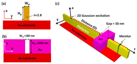
Figure 1.
Device architectures. (a) Cross-sectional view of a dielectric strip loaded on the Au substrate. (b) Cross-sectional view of a plasmonic trench waveguide. (c) Three-dimensional view of the input and output plasmonic couplers.
2. Simulation and Methodology
The modal field distribution and transmittance of the waveguide structures were computed by using a commercial software (Rsoft FullWAVE) based on the finite-difference time-domain (FDTD) method. In the FDTD simulations, the size of the Yee cells was 20 nm × 20 nm × 20 nm, and the time step followed the Courant–Friedrichs–Levy condition in order to minimize the numerical dispersion. The size of the Yee cells was far smaller than the excitation wavelength in a free space. We used 1550 nm as the excitation wavelength, which is the central wavelength of the long-haul telecommunication wavelength range. At the computational boundaries, perfectly matched layers (10 layers) [27] were used to minimize the reflections from the outgoing EM waves in order to simulate an infinite space. In other words, the input and output dielectric strips extended infinitely in the –z and +z directions, respectively. A two-dimensional (2D) Gaussian excitation (orange plate) was placed in the input TiO2 dielectric strip in order to match the modal profile of the rectangular dielectric waveguide, as shown in Figure 1c. The SPP waves in the plasmonic trench could be excited via the buttcoupling method [19,20] with the waveguide mode in the TiO2 dielectric strip when the electric field was perpendicular to the inner walls of the Au trench. The input and output TiO2 dielectric strips did not touch the plasmonic Au structure, with a gap distance of 50 nm. The small gap distance was required but was limited by the controllable linewidth in the electron beam lithography process. The TiO2 dielectric strips were loaded on the Au substrate. Wd and Hd are the width and height of the TiO2 strips, respectively. The refractive index of the dielectric strip was fixed at 2.8 in order to form a small modal size that could effectively excite the plasmonic waveguide at the sub-wavelength scale. The refractive index values of TiO2 crystals ranged from 2.6 to 2.8 in the transparent wavelength range [28]. The refractive index and extinction coefficient values of Au were 0.524 and 10.742 at λ0 = 1550 nm, respectively [29]. The electric field of the excitation was along the y-direction. Wm and Hm are the width and height of the plasmonic trench waveguide, respectively, which were both smaller than the excitation wavelength. To form a low-loss Au plasmonic trench waveguide, a small aspect ratio of the trench width and trench height was used [11]. Wm and Hm are 180 nm and 1000 nm, respectively. This predicted that the shorter trench height corresponded to the larger propagation loss owing to increased ohmic loss from the Au substrate. A time monitor (green plate) was placed in the output TiO2 dielectric strip in order to compute the transmittance, which could be used to evaluate the coupling efficiency between the dielectric waveguide and plasmonic waveguide. In addition, the instantaneous field distribution along the propagation direction of the waveguides could be used to compute the modal index values by using the fast Fourier transform technique.
3. Results and Discussion
Figure 2a presentsthe cross-sectional electric field (Ey) distributions of the dielectric strip loaded on the Au substrate and the Au plasmonic trench waveguide at the wavelength of 1550 nm, respectively. The excitations are located at z = 0. In the dielectric waveguide, the TiO2 strip is loaded on the Au substrate, which results in a zigzag propagation path under the 2D Gaussian excitation. The Wd and Hd of the TiO2 strip are 300 nm and 1000 nm, respectively. The period of the zigzag path is about 5 μm. In other words, the optical waves propagate along the TiO2 strip from the top (bottom) region to the bottom (top) region in the half period of a zigzag propagation. In the plasmonic trench waveguide, the electric field is mainly distributed in the top region of the trench, which forms a stable modal profile along the propagation direction, as indicated in the region of the dotted line rectangle of Figure 2a. Figure 2b plots the fast Fourier transform spectra of the Ey distributions in Figure 2a. The main peaks (λpeak) are located at 1.058 × 10⁶/m and 0.794 × 10⁶/m, respectively, which can be used to compute the modal index values of the two waveguides by using the relation n = λ0/λWG, where λ0 is the wavelength in a free space, and λWG is the wavelength in the waveguide. The calculated modal index values of the TiO2 strip waveguide loaded on the Au substrate and the Au plasmonic trench waveguide are 1.640 and 1.230, respectively. The modal index in the TiO2 strip is higher than that in the Au plasmonic trench even though the Wd is larger than the Wm. The main reason is that the dielectric waveguide mode and SPP mode mainly propagate in the high-index medium (TiO2) and low-index medium (air), respectively. It was predicted that the zigzag path in the TiO2 strip significantly influences the coupling efficiency between the dielectric waveguide and the plasmonic trench waveguide.
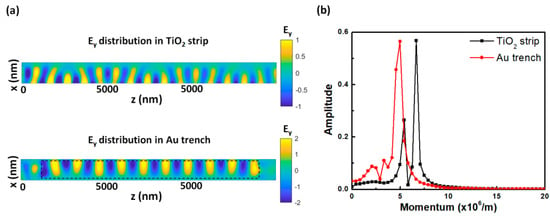
Figure 2.
(a) The instantaneous Ey distributions in the TiO2 strip waveguide loaded on the Au substrate and the Au plasmonic trench waveguide. (b) The fast Fourier transform spectra of the instantaneous Ex distributions.
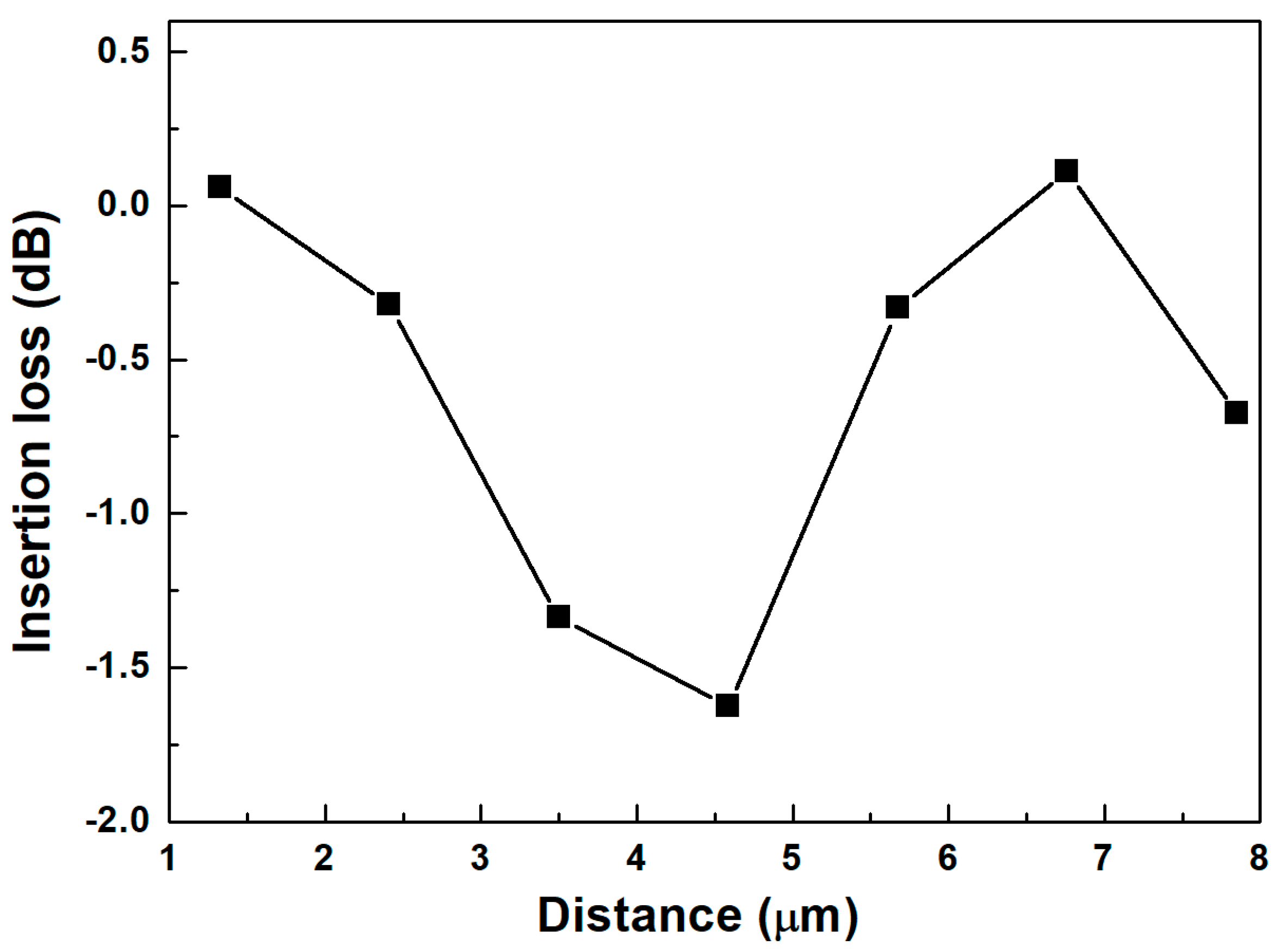
Figure 3 presents the distance-dependent insertion loss (IL) of the proposed dielectric–metallic–dielectric waveguide structure. The distance (D) is from the excitation plate to the entrance of the plasmonic trench waveguide, as shown in Figure 1c. The IL is computed by using the relation IL = 10log10(T), where T is transmittance. When the D values are 1.32 μm and 6.76 μm, the IL (T) values are 0.06 dB (101.4%) and 0.12 dB (102.6%). The difference between the two D values is 5.46 μm, which is close to the period of the zigzag propagation path in the TiO2 strip. When the D value is 4.59 μm, the IL (T) value is −1.63 dB (68.8%). The highest IL (lowest transmittance) is owing to the largest shift between the two modal profiles in the TiO2 strip and in the Au trench. In other words, the modal field overlap between the modal fields in the TiO2 strip and the Au plasmonic trench largely influences the coupling efficiency. It is noted that the IL values can be higher than 0 dB because the propagation loss of the Au plasmonic trench waveguide is lower than that of the TiO2 strip waveguide loaded on the Au substrate. The attenuation coefficient of the two waveguides can be computed by using the relation I(z) = I0exp(−αz), where I0 is the intensity at z = 0, and α is the absorption coefficient. In the waveguides, I(z) is proportional to |Ex(z)|2. According to the |Ex|2 distributions in Figure S2, the calculated α values of the TiO2 strip waveguide loaded on the Au substrate and the Au plasmonic trench waveguide are 10.35 × 10⁴/m and 1.22 × 10⁴/m, respectively.
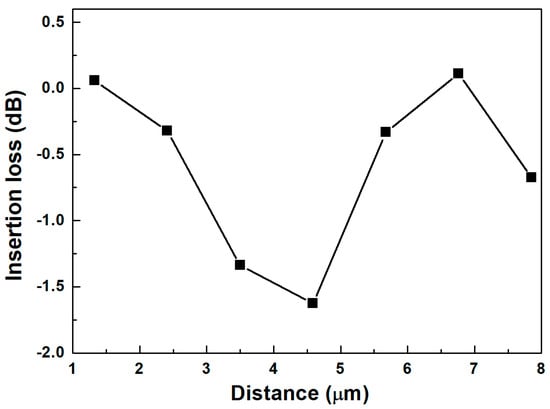
Figure 3.
Distance-dependent insertion loss of the proposed dielectric–metallic–dielectric waveguide structure. The Wd, Hd, Wm, and Hm are 300 nm, 1000 nm, 180 nm, and 1000 nm, respectively.
It is noted that the real part and imaginary part of the propagation constant (kR and kI) can be computed by using the relations kR = 2π/λpeak and kI = α/2. In addition, the kR/kI can be defined as the figure of merit (FOM) of the waveguide. The propagation characteristics of the two waveguides are listed in Table 1. The high FOM shows that the Au plasmonic trench waveguides can stand as the building blocks in the near-infrared OICs when the width and height are 180 nm and 1000 nm, respectively. The FOM of the Au plasmonic trench waveguide is about 771, which is higher than that of other plasmonic waveguides [30,31,32].

Table 1.
Propagation characteristics of the waveguides at λ0 = 1550 nm.
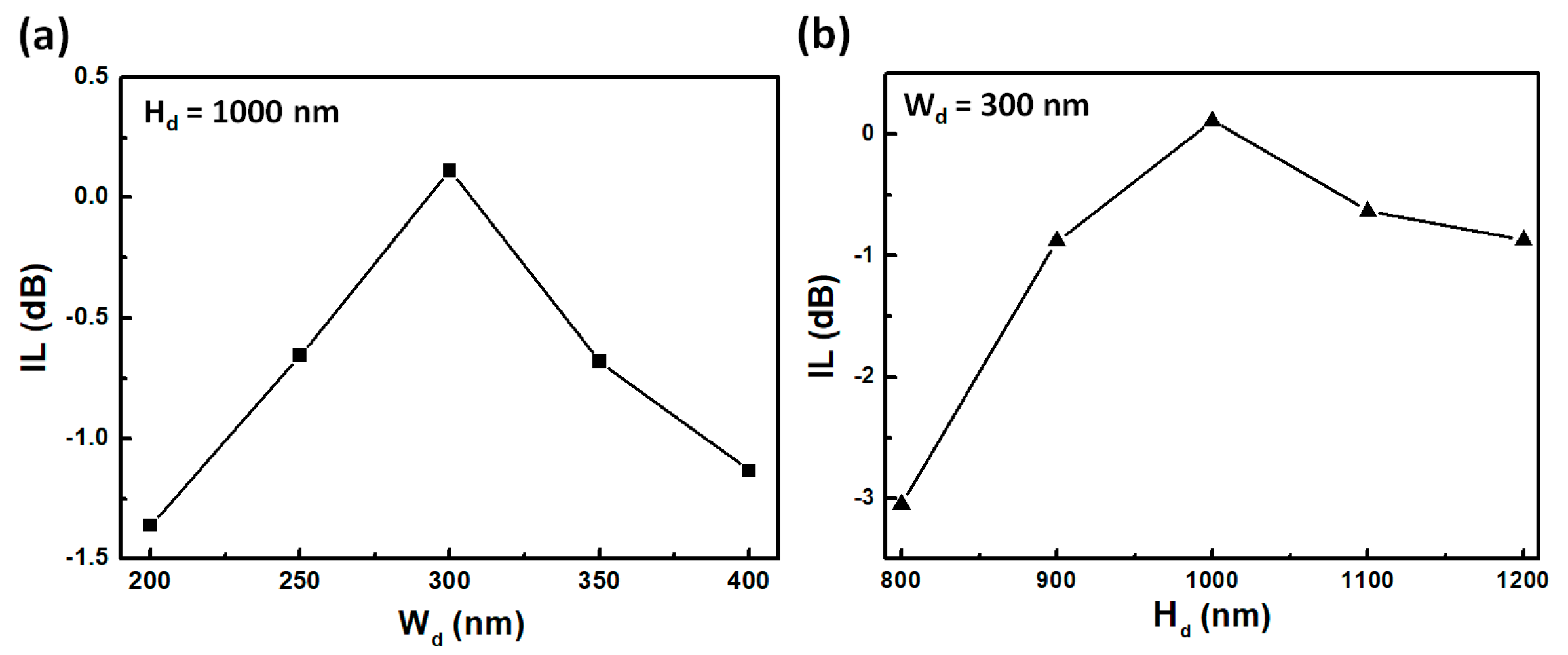
Figure 4 presents the IL of the proposed dielectric–metallic–dielectric waveguide structure with different Wd or Hd values while keeping the D value at 6.76 μm. When the Wd value increases from 200 nm (300 nm) to 300 nm (400 nm), the IL value changes from −1.36 dB (0.12 dB) to 0.12 dB (−1.13 dB). In Figure 4a, the curve is slightly left–right asymmetrical, centered at the Wd of 300 nm. When the Wd values are 400 nm and 200 nm, the IL values are −1.13 dB and −1.36 dB, respectively, which is due to the larger effective coupling area of the plasmonic waveguide [17,20]. The effect of the larger effective coupling also results in the anomalous light transmissions. Refs. [33,34] When the Hd value increases from 800 nm (1000 nm) to 1000 nm (1200 nm), the IL value changes from −3.05 dB (0.12 dB) to 0.12 dB (−0.87 dB). In Figure 4b, the curve has a strong left–right asymmetry centered at the Hd of 1000 nm. When the Hd value is 800 nm, the modal fields in the TiO2 strip and the Au trench have a large shift in the vertical direction, thereby resulting in the low coupling efficiency. When the Hd value is 1200 nm, the modal fields in the TiO2 strip and the Au trench can be better matched in the vertical direction, thereby resulting in the relatively higher coupling efficiency. When the D value is fixed at 6.76 μm, the optimal Wd and Hd values are 300 nm and 1000 nm, respectively, which is mainly due to the modal-field match between the TiO2 strip and Au trench in the vertical direction. Conceptually, the period of the zigzag propagation path in the TiO2 strip waveguide loaded on the Au substrate is related to the Wd and Hd. In other words, the optimal distance for the lowest IL is related to the Wd and Hd. Therefore, it is possible to increase the coupling efficiency after optimizing the D, Wd, and Hd values simultaneously. It is noted that the D, Wd, and Hd values must be re-optimized when the Wm or Hm is changed.
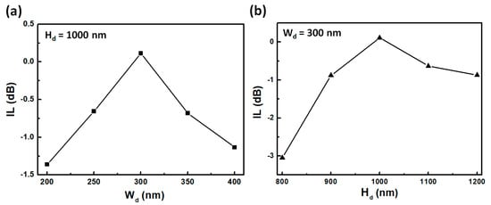
Figure 4.
(a) Wd-dependent insertion loss (IL) of the proposed dielectric–metallic–dielectric waveguide structure. (b) Hd-dependent IL of the proposed dielectric–metallic–dielectric waveguide structure. The distance (D) and wavelength are 6.76 μm and 1.55 μm, respectively.
On the other hand, the modal field in the TiO2 strip can be up-shifted by using a thin cladding layer on the TiO2 strip in order to increase the coupling efficiency. However, the use of a cladding layer will change the period of the zigzag propagation path in the TiO2 strip waveguide loaded on the Au substrate, which also influences the optimal distance for the lowest IL. In other words, the modal-field match in the vertical direction can be obtained after optimizing the thickness (refractive index) of the cladding layer and the optimal distance simultaneously.
4. Conclusions
In summary, we have theoretically investigated the coupling efficiency between TiO2 strips on an Au substrate and an Au plasmonic trench waveguide at the wavelength of 1550 nm. When the width (height) of the dielectric strip is 300 nm (1000 nm), the optimal distance between the excitation source and the entrance to the plasmonic waveguide is 6.76 μm, which effectively reduces the coupling loss, thereby forming a nearly 100% coupling efficiency. It is noted that the optimal distance is highly related to the period of the zigzag propagation path in the input TiO2 strip.
Supplementary Materials
The following supporting information can be downloaded at https://www.mdpi.com/article/10.3390/photonics11070608/s1, Figure S1: Fabrication methods: (a–f) top view; (g–l) side view; (b,h) photolithography, dry etching, and thermal evaporation; (c,i) photolithography and dry etching; (d,j) photolithography and dry etching; (e,k) oxidation;(f,l) photolithography and sputter. Figure S2: |Ex|2 distributions of the TiO2 strip waveguide loaded on the Au substrate and the Au plasmonic trench waveguide at the wavelength of 1550 nm.
Author Contributions
Conceptualization, S.H.C.; data curation, J.-R.W.; formal analysis, S.H.C., J.-R.W. and A.C.; supervision, S.H.C. and C.C.; writing—original draft, S.H.C. and J.-R.W.; writing—review and editing, S.H.C. and C.C. All authors have read and agreed to the published version of the manuscript.
Funding
This research was funded by the National Science and Technology Council, Taiwan. The grant numbers are NSTC 110-2112-M-033-012-MY3, NSTC 111-2112-M-033-008, and NSTC 110-2112-M-033-009-MY3.
Data Availability Statement
The data presented in this study are available on request from the corresponding author.
Conflicts of Interest
The authors declare no conflicts of interest.
References
- Anwar, R.S.; Ning, H.; Mao, L. Recent advancements in surface plasmon polaritons-plasmonics in subwavelength structures in microwave and terahertz regimes. Digit. Commun. Netw. 2018, 4, 244–257. [Google Scholar] [CrossRef]
- Kim, J.T.; Park, S.; Ju, J.J.; Lee, S.; Kim, S. Low bending loss characteristics of hybrid plasmonic waveguide for flexible optical interconnect. Opt. Express 2010, 18, 24213–24220. [Google Scholar] [CrossRef]
- Tai, C.-Y.; Chang, S.H.; Chiu, T. Design and analysis of an ultra-compact and ultra-wideband polarization beam splitter based on coupled plasmonic waveguide arrays. IEEE Photonics Technol. Lett. 2007, 19, 1448–1450. [Google Scholar] [CrossRef]
- Liou, F.; Dai, D.; Wosinski, L. Ultracompact polarization beam splitter based on a dielectric-hybrid plasmonic-dielectric coupler. Opt. Lett. 2012, 37, 3372–3374. [Google Scholar] [CrossRef]
- Tai, C.-Y.; Yu, W.-H.; Chang, S.H. Giant angular dispersion mediated by plasmonic modal competition. Opt. Express 2010, 18, 24510–24515. [Google Scholar] [CrossRef]
- Jun, Y.C.; Huang, K.C.Y.; Brognersma, M.L. Plasmonic beaming and active control over fluorescent emission. Nat. Commun. 2011, 2, 283. [Google Scholar] [CrossRef]
- Gan, Q.; Gao, Y.; Bartoli, F.J. Vertical plasmonic Mach-Zehnder interferometer for sensitive optical sensing. Opt. Express 2009, 17, 20747–20755. [Google Scholar] [CrossRef]
- Gao, Y.; Gan, Q.; Xin, Z.; Cheng, X.; Bartoli, F.J. Plasmonic Mach-Zehnder interferometer for ultrasensitive on-chip biosensing. ACS Nano 2011, 5, 9836–9844. [Google Scholar] [CrossRef] [PubMed]
- Lu, H.; Liu, X.; Mao, D.; Wang, L.; Gong, Y. Tunable band-pass plasmonic waveguide filters with nanodisk resonators. Opt. Express 2010, 18, 17922–17927. [Google Scholar] [CrossRef]
- Zhuang, H.; Kong, F.; Li, K.; Sheng, S. Plasmonic bandpass filter based on graphene nanoribbon. Appl. Opt. 2015, 54, 2558–2564. [Google Scholar] [CrossRef]
- Chang, S.H.; Chiu, T.C.; Tai, C.-Y. Propagation characteristics of the supermode based on two coupled semi-infinite rib plasmonic waveguides. Opt. Express 2007, 15, 1755–1761. [Google Scholar] [CrossRef] [PubMed]
- Gramotnev, D.K.; Bozhevolnyi, S.I. Plasmonics beyond the diffraction limit. Nat. Photonics 2010, 4, 83–91. [Google Scholar] [CrossRef]
- Huong, N.T.; Chinh, N.V.; Hoang, C.M. Wedge surface Plasmon polariton waveguides based on wet-bulk micromachining. Photonics 2019, 6, 21. [Google Scholar] [CrossRef]
- Liao, Y.-S.; Wu, J.-R.; Thakur, D.; Hsu, J.-S.; Dwivedi, R.P.; Chang, S.H. Power loss reduction of angled metallic wedge plasmonic waveguides via the interplay between near-field optical coupling and modal coupling. Photonics 2022, 9, 663. [Google Scholar] [CrossRef]
- Kewes, G.; Schoengen, M.; Neitzke, O.; Lombardi, P.; Schonfeld, R.-S.; Mazzamuto, G.; Schell, A.W.; Probst, J.; Wolters, J.; Lochel, B.; et al. A realistic fabrication and design concept for quantum gates based on single emitters integrated in plasmonic dielectric waveguides structures. Sci. Rep. 2016, 6, 28877. [Google Scholar] [CrossRef] [PubMed]
- Zhang, M.; Hu, G.; Zhang, S.; Gao, D.; Sun, Y.; Wang, F. Gain characteristics of the hybrid solt waveguide amplifiers integrated with NaYF4:Er3+ NPs-PMMA covalently linked nanocomposites. RSC. Adv. 2020, 10, 11148–11155. [Google Scholar] [CrossRef] [PubMed]
- Veronis, G.; Fan, S. Theoretical investigation of compact couplers between dielectric slab waveguides and two-dimensional metal-dielectric-metal plasmonic waveguides. Opt. Express 2007, 15, 1211–1221. [Google Scholar] [CrossRef] [PubMed]
- Tian, J.; Yu, S.; Yan, W.; Qiu, M. Broadband high-efficiency surface-plasmon-polariton coupler with silicon-metal interface. Appl. Phys. Lett. 2009, 95, 013504. [Google Scholar] [CrossRef]
- Berini, P. Long-range surface Plasmon polaritons. Adv. Opt. Photonics 2009, 1, 484–588. [Google Scholar] [CrossRef]
- Chang, S.H.; Tai, C.-Y. Broadband energy conversion between off-plane Gaussian lightwave and in-plane surface Plasmon waves. IEEE Photonics Technol. Lett. 2011, 23, 1727–1729. [Google Scholar] [CrossRef]
- Manfrinato, V.R.; Zhang, L.; Su, D.; Duan, H.; Hobbs, R.G.; Stach, E.A.; Berggren, K.K. Resolution limits of electron-beam lithography toward atomic scale. Nano. Lett. 2013, 13, 1555–1558. [Google Scholar] [CrossRef] [PubMed]
- Wongwanitwattana, C.; Shah, V.A.; Myronov, M.; Parker, E.H.C.; Whall, T.; Leadley, D.R. Precision plasma etching of Si, Ge, and Ge:P by SF6 with added O2. J. Vac. Sci. Technol. A 2014, 32, 031302. [Google Scholar] [CrossRef]
- Mahmoodi, N.; Rushdi, A.I.; Bowen, J.; Sabouri, A.; Anthony, C.; Mendes, P.M.; Preece, J.A. Room temperature thermally evaporated thin Au film on Si suitable for application of thiol self-assembled monolayers in micro-nano-electro-mechanical-systems sensors. J. Vac. Sci. Technol. A 2017, 35, 041514. [Google Scholar] [CrossRef]
- Wright, J.T.; Carbaugh, D.J.; Haggerty, M.E.; Richard, A.L.; Ingram, D.C.; Kaya, S.; Jadwisienczak, W.W.; Rahman, F. Thermal oxidation of silicon in a residual oxygen atmosphere-the RESOX process-for self-limiting growth of thin silicon dioxide films. Semicond. Sci. Technol. 2016, 31, 105007. [Google Scholar] [CrossRef]
- Heo, C.H.H.; Lee, S.-B.; Boo, J.-H. Deposition of TiO2 thin films using RF magnetron sputtering method and study of their surface characteristics. Thin Solid Films 2005, 475, 183–188. [Google Scholar] [CrossRef]
- Dong, B.; Ma, Y.; Ren, Z.; Lee, C. Recent progress in nanoplasmonics-based integrated optical micro/nano-systems. J. Phys. D Appl. Phys. 2020, 53, 213001. [Google Scholar] [CrossRef]
- Udagedara, I.; Premaratne, M.; Rukhlenko, I.D.; Hattori, H.T.; Agrawal, G.P. Unified perfectly matched layer for finite-difference time-domain modeling of dispersive optical materials. Opt. Express 2009, 17, 21179–21190. [Google Scholar] [CrossRef]
- Jolivet, A.; Labbe, C.; Frilay, C.; Debieu, O.; Marie, P.; Horcholle, B.; Lemarie, F.; Portier, X.; Grygiel, C.; Duprey, S.; et al. Structural, optical, and electrical properties of TiO2 thin films deposited by ALD: Impact of the substrate, the deposited thickness and the deposition temperature. Appl. Surf. Sci. 2023, 608, 155214. [Google Scholar] [CrossRef]
- Johnson, P.B.; Christy, R.W. Optical constants of the noble metals. Phys. Rev. B 1972, 6, 4370–7379. [Google Scholar] [CrossRef]
- Qin, X.; He, Y.; Sun, W.; Fu, P.; Wang, S.; Zhou, Z.; Li, Y. Stepped waveguide metamaterials as low-loss effective replica of surface Plasmon polaritons. Nanophotonics 2023, 12, 1285–1293. [Google Scholar] [CrossRef]
- Shneen, W.F.; Ameen, S.M.M. Controllable surface Plasmon polariton propagation length using a suitable quantum dot material. Braz. J. Phys. 2024, 54, 59. [Google Scholar] [CrossRef]
- Chaparala, R.; Imamavali, S.; Tupakula, S. Enhancement of spoof surface plasmon polariton waveguide performance through modified groove width. Opt. Eng. 2024, 63, 055102. [Google Scholar] [CrossRef]
- Schouten, H.F.; Visser, T.D.; Lenstra, D.; Blok, H. Light transmission through a subwavelength slit: Waveguiding and optical vortices. Phys. Rev. E 2003, 67, 036608. [Google Scholar] [CrossRef] [PubMed]
- Sturman, B.; Podivilov, E.; Gorkunov, M. Theory of extraordinary light transmission through arrays of subwavelength slits. Phys. Rev. B 2008, 77, 075106. [Google Scholar] [CrossRef]
Disclaimer/Publisher’s Note: The statements, opinions and data contained in all publications are solely those of the individual author(s) and contributor(s) and not of MDPI and/or the editor(s). MDPI and/or the editor(s) disclaim responsibility for any injury to people or property resulting from any ideas, methods, instructions or products referred to in the content. |
© 2024 by the authors. Licensee MDPI, Basel, Switzerland. This article is an open access article distributed under the terms and conditions of the Creative Commons Attribution (CC BY) license (https://creativecommons.org/licenses/by/4.0/).

