Abstract
Lithography variation presents one of the biggest challenges for photonic component optimization, especially for fabless designers. Lithography prediction models are a crucial tool for minimizing the necessary number of fabrication iterations for a device’s optimization. This paper presents one of these models specifically adapted for the contra-directional coupler structure. Through the experimental characterization of devices with a specific range of design parameters, it was possible to observe how the lithography process impacts their performance. A correction model based on effective refractive index variation and its impact on the Bragg condition of the structure was developed to predict the performance variation of a device based on the expected design variation induced by fabrication. The contra-directional couplers fabricated at CORNERSTONE foundry show a tendency to be redshifted as the gap decreases, due to an increase in waveguide width as a result of a diffraction-limited lithography process. Based on these and other findings, it was possible to correlate the design parameters to the posterior fabricated structure and ultimately predict the expected experimental response.
1. Introduction
Photonic component simulation and optimization is a fundamental step for photonic integrated circuit (PIC) design, as it provides the necessary building blocks for system implementation. Novel solutions can often enable and lead to the conception of new architectures that are simpler and cheaper. However, when dealing with these novel components, the challenge of tuning their response increases due to the lack of previous experimental data. It is expected that a building block provided in a foundry Process Design Kit (PDK) will have the stated response. This is so due to the numerous previous iterations of optimization done by the foundry or PDK provider, that have made possible the correction of the geometry of the component based on the experimental data and deep knowledge of the impact of the lithography effects of that same foundry on the structures.
For the fabless component designer, it is only possible to study in advance the general known impacts that each lithography technique is expected to induce upon the component structure and simulate accounting for it. In the case of photolithography, corner rounding effects that smooth small rectangular shapes, and proximity effects that translate in variations of the fabricated structures according to the presence and distance of the features around them, are extremely hard to account for, since they are the result of the limitations of the system’s resolution [1].
As for an expected lithography bias (as in the systematic error subsequent of the system equipment that can be accounted for) if the foundry provides ranges of anticipated thickness variation and width variation (typically associated with the width of the single mode waveguide recommended for their fabrication stack), those are usually in the order of tens of nanometers, which makes the optimization of the devices challenging, especially for those which are more sensitive to fabrication error [2].
A contra-directional coupler (contra-DC) is a device composed of two parallel waveguides in close proximity, each with periodic sidewall corrugations, combining the characteristics of a Bragg grating and a directional coupler forming a 4-port device. Due to the corrugations in the waveguides, the optical signal travelling the device will experience partial reflections, as illustrated in Figure 1. As such, constructive interference will arise for wavelengths that satisfy the Bragg condition, resulting in a backward-propagating mode that will couple into the second waveguide, into a separate port (drop) from the input and through ports in the first waveguide [3,4].
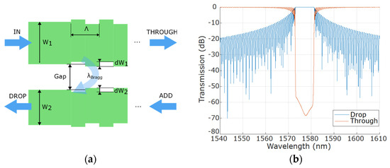
Figure 1.
(a) Structure diagram and (b) typical simulated spectral response of a contra-DC [2].
Although this component presents clear advantages in comparison to other demultiplexing structures or systems, like the elimination of free spectral range and input and output signal separation within a single structure, it is highly sensitive to fabrication deviation, due to the implementation of a narrow gap (with typical values of 150–250 nm) between waveguides and corrugations on both edges of both waveguides (values around 30 nm to 90 nm in height and 75 to 150 nm in width). It also has a very limited response variation to applied active tuning [5,6]. It is therefore extremely hard to optimize with no previous experimental data to derive from, and impossible if a correction model is not even used.
This paper proposes the divulgation of a model correlating the response variation of the contra-DC device with the studied experimental variation in the fabricated geometry, therefore cutting the number of iterations to achieve the tuned desired response. Since the final equation was obtained through experimental data from devices fabricated at the CORNERSTONE foundry (Southampton, UK), it can only be used with no extra tuning for devices fabricated using the same facilities. Otherwise, the parameters of the provided general model need to be adjusted based on the experimental results obtained from a first iteration of contra-DC test devices in the foundry of interest.
The correction model presented in this paper is intended as an aiding tool for all fabless designers who wish to optimize the Contra-DC structure for their required needs. The changes in the effective refractive index of the waveguide modes upon geometrical variations of the structure are the considered origin of the response variation as a consequence of lithographic effects. It is this phenomenon that the model was built upon [1].
2. Methodology
To understand the effect of the gap in a contra-DC’s response and the impact of the fabrication process on this parameter, several contra-DCs were designed by systematically varying the gap between waveguides while keeping the remaining design parameters unchanged. The 9 devices have gaps of 200, 210, 230, 250, 260, 270, 290, 310 and 320 nm, waveguide widths of 450 and 350 nm, corrugation sizes of 80 and 40 nm and pitches of 319 nm.
The devices were simulated using the open source SIEPIC contra-DC simulator package that makes use of Ansys Lumerical EME solver [7], where the spectral response was observed, and the central wavelength and 3 dB bandwidth were extracted. These figures of merit were extracted in a similar manner to what is presented in Figure 2, where the central wavelength is the center of the pass-band of the drop port spectrum while the 3 dB bandwidth is the spectral width at which the maximum power of the pass-band drops to half.
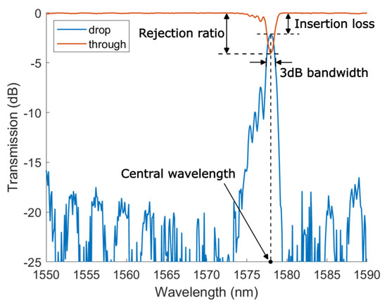
Figure 2.
Experimental spectral response of a contra-DC and its figures of merit.
In these initial simulations, the central wavelength does not present a significant variation, changing only 0.4 nm across all devices. On the contrary, the 3 dB bandwidth decreases linearly as the gap increases, which is associated with the decreasing coupling strength. These tendencies can be observed in the graphs present in Figure 3.
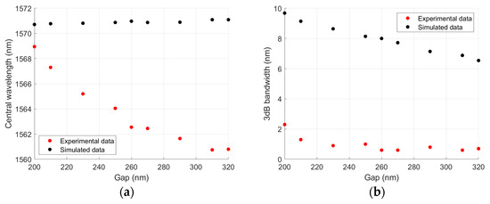
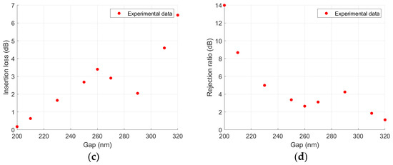
Figure 3.
Experimental results of (a) central wavelength, (b) 3 dB bandwidth, (c) insertion loss and (d) rejection ratio with gap variation.
The fabrication of the devices took place in a multi-project wafer service provided by CORNERSTONE foundry using 248 nm dry photolithography (KrF light source) and a silicon-on-insulator platform with 220 nm rib waveguides, with a slab of 100 nm. The structures were etched using a dry etching process in an inductively coupled plasma (ICP) etching tool.
3. Experimental Characterization
The devices were characterized through grating couplers using a broadband source and an optical spectrum analyzer at the input and output, respectively. The drop and through spectra were acquired. Figure 2 shows an example of a device’s spectra and the relevant figures of merit calculated.
The results for central wavelength, 3 dB bandwidth, insertion loss and rejection ratio can be seen in Figure 3. Analyzing the central wavelength behavior, it is evident that the central wavelength tends to decrease as the gap widens.
It is plausible to assume that the lithography process is the source of the central wavelength variation seen in experimental data, as this variation is not anticipated by the simulation. Seeing how the two design parameters that influence the central wavelength are the pitch and the waveguide widths, one of these factors is most likely being affected by the lithography process.
The 3 dB bandwidth shows that the experimental values are significantly reduced compared to what was observed in simulation, thus implying that one or more of the design parameters that impact this figure of merit—the gap and the corrugations—are also being affected in the fabrication process. Furthermore, the 3 dB bandwidth does not present the linear behavior that is seen in simulation and its value is constant from gaps wider than 260 nm.
Looking at the insertion loss and the rejection ratio, it is possible to identify two coupling regimes: for smaller gaps, the insertions loss increases at a slower rate while the rejection ratio is still high. However, as the gap increases, the insertion loss increases more rapidly, and the rejection ratio becomes significantly reduced. This behavior shows how the device loses its coupling strength as the gap widens, reaching a point where no radiation is able to couple into the second waveguide for gaps bigger than 320 nm.
To understand what phenomenon could be taking place in the fabrication process to affect the devices and trigger these behavior-alteration trends common to all runs and foundries, the topography of devices fabricated in a different foundry run was analyzed through scanning electron microscopy (SEM), and their design parameters were extracted as exemplified in Figure 4.
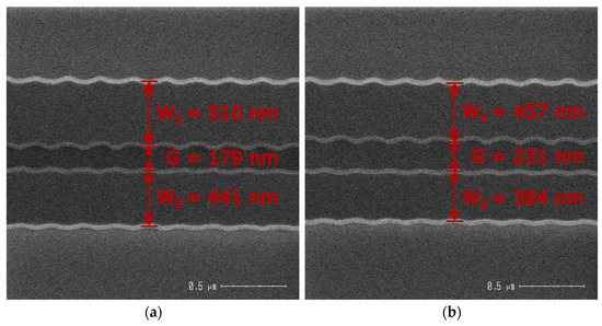
Figure 4.
SEM images of contra-DCs with (a) smaller and (b) wider gap (G) and its impact on the waveguide widths (W1 and W2).
The most noticeable observation is that the corrugations suffer from smoothing effect and their shape becomes sinusoidal instead of squared, due to the optical diffraction of the UV source when passing through the mask [1]. Immediately, this helps to explain the decrease in 3 dB bandwidth for all the gap parameter values, since the gap between waveguides becomes enlarged and the corrugation widths smaller. Additional inspection shows that the gap parameter significantly impacts the widths of the waveguides, with the first waveguide widening 53 nm and the second widening 57 nm when the gap closes by 52 nm. With these results, it is possible to infer that smaller gaps indirectly make the waveguide widths larger in the fabrication process, thus increasing the effective refractive index of the waveguides and, consequently, their central wavelength, a trend that is not observed in the simulated data, because the simulated waveguide widths remained constant with the variation of the gap parameter.
This phenomenon is attributed to the proximity effect mentioned in the introduction. The variation of the designed gap parameter value becomes a factor that influences the resulting waveguide structures, since according to the proximity effect, these features are highly dependent on their immediate environment due to the optical diffraction limits of the DUV system.
4. Simulation Model Validation
The lithographic phenomenon previously proposed was simulated using Ansys Lumerical MODE solver, in a similar way to the initial device simulations mentioned in Section 2, to understand if the scenario is valid and evaluate how much the design would have to change to obtain the experimental results.
The first step of the process was to reach the design parameters that would yield the optical response observed for the device with the widest gap (320 nm). The waveguide widths were reduced by 24.5 nm and the corrugation sizes were reduced to 25% of their original size to reach in simulation the experimentally obtained central wavelength of 1560.7 nm and 3 dB bandwidth of 0.7 nm.
After achieving the parameters of the first device, the remaining devices with the decreasing gap parameter had their waveguide widths gradually incremented on the inner side of the gratings, proportionally to the decrease in gap, in order to replicate the effect of the worse etching as the gap decreases. The central wavelength response of all devices was found by changing only the waveguide width in this manner, and the resulting curve of width values as a function of the gap was fitted through different models, such as linear, exponential, logarithmic, etc., to assess the best fitting scenario.
It was found that the best fitting case was exponential and, thus, it is possible to conclude that the waveguide width variation as a function of the gap, resulting from the etching variation in the fabrication process, can be related through Equation (1).
where is the increase in waveguide width dependent on the gap parameter and is the smallest gap.
This model describes a trend in experimental central wavelength results due to lithographic variation that is commonly present in fabricated contra-DCs and, therefore, can be adapted to other components fabricated in different foundries. For the experimental results shown in Figure 3a, fitting parameters of , and were obtained.
To adapt this model and optimize it for other possible foundries and devices, a test run in the foundry of interest must be done with devices of different gap values. The experimental central wavelength response of these devices then needs to be measured, and its variation must be translated into a waveguide width difference. This can be done by adjusting the waveguide widths as a function of the gap in order to replicate, in the simulator, the experimental response observed for each device. After having these waveguide width values, the trend can be fitted using Equation (1), which will yield the experimental variation of waveguide width experienced by the devices due to the fabrication. Taking the resulting equation into account in simulation, the central wavelength response of the simulated devices should replicate, with greater accuracy, the response of the experimental devices by considering expected impacts due to lithography errors.
The results obtained through this model are present in Figure 5, where it is visible that the simulations present similar results to what was obtained experimentally, with a correlation coefficient of between the experimental and simulation central wavelength data. This means that the hypothesis proposed to explain the experimental behavior observed in the devices with different gaps is valid.
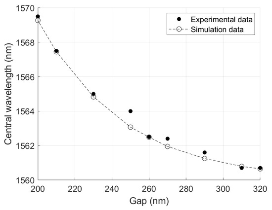
Figure 5.
Central wavelength simulation results compared to experimental data.
From these results, it is possible to conclude that narrower gaps cause significant lithographical variations, which are unforeseen in simulation. Given these findings, when designing future devices, this phenomenon must be considered, seeing as how a gap difference of only a few tens of nanometers can induce a central wavelength variation much larger than what can be tolerated considering wavelength demultiplexing applications.
5. Conclusions
This paper aimed to understand the impact of the lithography process on a contra-DC’s response, stemmed from a change in the gap parameter of the device. Through the experimental characterization of devices with several different gaps and the analysis of crucial SEM images of similar devices, it was possible to identify a lithography effect in the fabrication of contra-DCs that caused the waveguide widths to increase as the gap decreases.
These findings allowed the development of a rule-based correction model relating the experimental central wavelength shift of a contra-DC and the respective design parameters that presented a between the observed experimental response and the simulation results. The model confirmed that a waveguide width variation influenced by the gap parameter of a contra-DC, an effect that stems from the fabrication process of these devices, would yield the experimental response observed.
Ultimately, this paper serves as a rule-based corrective model intended to be used by fabless photonic designers, especially those without the resources to access commercial lithography simulation software (like Synopsys® S-Litho or Siemens® Calibre used for lithography prediction and correction in [5]), in their pursuit of minimizing lithographical variations that may change their designs and hinder the device’s intended response. Furthermore, this model may also be used to calibrate well-known lithography software, by introducing this case of contra-DCs as an example for optical proximity effect correction.
Author Contributions
Conceptualization, I.V., J.T. and A.T.; methodology, I.V. and M.J.C.; software, I.V., J.T., M.J.C. and J.S.; validation, I.V., J.T. and A.T.; formal analysis, I.V., J.T. and A.T.; investigation, I.V.; resources, A.T.; data curation, I.V.; writing—original draft preparation, I.V. and J.T.; writing—review and editing, I.V. and J.T.; visualization, I.V.; supervision, A.T.; project administration, A.T.; funding acquisition, A.T. All authors have read and agreed to the published version of the manuscript.
Funding
This work was performed under the PIC-FAST project co-funded by HORIZON.3.1—The European Innovation Council (EIC) with Grant Agreement No. 101145256, and under the Agenda Microeletrónica project, funded by Plano de Recuperação e Resiliência (PRR), with operation code 02/C05-i01.01/2022.PC644916358-00000028.
Institutional Review Board Statement
Not applicable.
Informed Consent Statement
Not applicable.
Data Availability Statement
The raw data supporting the conclusions of this article will be made available by the authors on request.
Acknowledgments
The University of Southampton and the UK Engineering and Physical Sciences Research Council (EPSRC) funded CORNERSTONE project (EP/L021129/1), CORNERSTONE 2 project (EP/T019697/1) or CORNERSTONE 2.5 project (EP/W035995/1).
Conflicts of Interest
The authors declare no competing interests. The authors Inês Venâncio, Joana Tátá, António Teixeira and João Santos were employed by the company PICadvanced, S.A. There is no conflict of interest between any of the authors and the company PICadvanced, S.A.
References
- Bogaerts, W.; Bradt, P.; Vanholme, L.; Bienstman, P.; Baets, R. Closed-Loop Modeling of Silicon Nanophotonics from Design to Fabrication and Back Again. Opt. Quantum Electron. 2008, 40, 801–811. [Google Scholar] [CrossRef]
- Venâncio, I.; Tátá, J.; Santos, J.; Duarte, P.; Rodrigues, C.; Teixeira, A. Impact of Process Variations on the Performance of Wavelength Dependent Devices. In Optical Waveguides and Related Technology; Kim, K.Y., Ed.; IntechOpen: London, UK, 2024; ISBN 978-0-85014-427-7. [Google Scholar]
- Shi, W.; Veerasubramanian, V.; Plant, D.V.; Jaeger, N.A.F.; Chrostowski, L. Silicon Photonic Bragg—Grating Couplers for Optical Communications. In Proceedings Volume 9010, Next-Generation Optical Networks for Data Centers and Short-Reach Links; Srivastava, A.K., Ed.; SPIE: Bellingham, WA, USA, 2014; p. 90100F. [Google Scholar] [CrossRef]
- Chrostowski, L.; Hochberg, M.E. Silicon Photonics Design; Cambridge University Press: Cambridge, UK, 2015; ISBN 978-1-107-08545-9. [Google Scholar]
- Lin, S.; Hammood, M.; Yun, H.; Luan, E.; Jaeger, N.A.F.; Chrostowski, L. Computational Lithography for Silicon Photonics Design. IEEE J. Sel. Top. Quantum Electron. 2020, 26, 8201408. [Google Scholar] [CrossRef]
- Cauchon, J. Silicon Photonic Bragg-Based Devices: Hardware and Software; Laval University: Quebec, QC, Canada, 2021. [Google Scholar]
- Hammood, M. SIEPIC Contra-DC Simulator 2023. Available online: https://github.com/SiEPIC/contraDC (accessed on 19 August 2024).
Disclaimer/Publisher’s Note: The statements, opinions and data contained in all publications are solely those of the individual author(s) and contributor(s) and not of MDPI and/or the editor(s). MDPI and/or the editor(s) disclaim responsibility for any injury to people or property resulting from any ideas, methods, instructions or products referred to in the content. |
© 2024 by the authors. Licensee MDPI, Basel, Switzerland. This article is an open access article distributed under the terms and conditions of the Creative Commons Attribution (CC BY) license (https://creativecommons.org/licenses/by/4.0/).