Article

Simulation Study on Tunable Terahertz Bandpass Filter Based on Metal–Silicon–Metal Metasurface

1
Chengdu Huanyuxin Technology Co., Ltd., Chengdu 610095, China
2
School of Precision Instruments and Opto-Electronics Engineering, Tianjin University, Tianjin 300072, China
*
Author to whom correspondence should be addressed.
Photonics 2024, 11(6), 559; https://doi.org/10.3390/photonics11060559
Submission received: 24 May 2024 / Revised: 10 June 2024 / Accepted: 12 June 2024 / Published: 13 June 2024
(This article belongs to the Special Issue Metamaterials for Terahertz Photonics: Enabling Novel Techniques)

Abstract

:
Metasurface devices have demonstrated powerful electromagnetic wave manipulation capabilities. By adjusting the shape and size parameters of the metasurface microstructure, we can control the resonance between spatial electromagnetic waves and the metasurface, which will trigger wave scattering at a specific frequency. By utilizing these characteristics, we design a metasurface device with a bandpass filtering function and a unit cell of the metasurface consisting of a double-layer pinwheel-shaped metal structure and high resistance silicon substrate (forming metal–silicon–metal configuration). A bandpass filter operating in the terahertz band has been implemented, which achieves a 36 GHz filtering bandwidth when the transmission amplitude decreases by 3 dB and remains effective in a wave incidence angle of 20°. This work uses an equivalent RC resonance circuit to explain the formation of bandpass filtering. In addition, the photosensitive properties of silicon enable the filtering function of the device to have on/off tuned characteristics under light excitation, which enhances the dynamic controllability of the filter. The designed device may have application prospects in 6G space communication.

1. Introduction

In recent years, 6G communication based on terahertz waves has attracted widespread attention [1]. The frequency of terahertz waves is higher than that of existing microwave communication. Therefore, terahertz waves have faster data transmission rates and larger data capacity. Space electromagnetic wave filters are one of the key functional devices in the field of wireless communication. With the development of 6G communication, the demand for space terahertz wave filters is obviously increasing. A terahertz filter with small size, easy integration, and rich functionality is expected.
A metasurface is a powerful special device [2,3,4,5,6,7], and its basic unit is a subwavelength artificial microstructure, which periodically expands in space to form a metasurface. Metasurfaces have been proven to have powerful electromagnetic wave manipulation capabilities. The physical characteristics of electromagnetic waves, such as frequency, phase, amplitude, polarization, orbital angular momentum, and spin angular momentum [8,9,10,11,12,13], can be manipulated by metasurfaces, enabling a variety of functions, including electromagnetic polarization transformation, wavefront manipulation [14], imaging [15], sensing [16,17], filtering [18,19,20], and so on. Among them, the filtering characteristics of the metasurface are controlled by the resonance between electromagnetic waves and the metasurface. By adjusting the shape and size of the metasurface microstructure, we can control the resonance between spatial electromagnetic waves and the metasurface. This resonance effect will trigger the reflection, transmission, and absorption of waves at specific frequencies. For instance, Zhao et al. [18] proposed a multi-layer metal structure consisting of a cross-shaped and open ring based on bandpass filtering theory. This structure achieves reflective C-band bandpass filtering with a polarization conversion function. Also, Ali Lalbakhsh et al. [19] proposed a simpler metal structure that uses two identical pinwheel structures to achieve polarization independent transmission bandpass filtering capability. The device was successfully demonstrated in the X-band. Amirashkan Darvish et al. [20] simultaneously proposed a flexible metasurface filter in which a unit cell consisting of two conductive rings and a flexible substrate is designed to achieve X-band filtering in a bent state. Generally, compared to traditional filters, metasurface filters have significant advantages, including small size, customizability, and rich functionality. The current development of metasurface filters is toward functional diversity, which is not only beneficial for further reducing the volume of communication systems but may also generate more novel applications.
In this work, a bandpass-filtered metasurface device with the interaction between two adjacent resonances is designed based on a double-layer pinwheel-shaped metal cell and a substrate with high resistance silicon. The effective filtering range of this device is 167–203 GHz. When the transmission amplitude decreases by 3 dB, it has a filtering bandwidth of 36 GHz and a maximum transmission amplitude of 0.9. These characteristics are effective within a wave incidence angle of 20°. This work uses an equivalent RC resonance circuit to explain the formation of bandpass filtering. Furthermore, compared to previous reports [18,19,20], this work achieves a bandpass filter with a dynamic on/off tuning function, where the photosensitive characteristics of silicon are used to modify the carrier concentration of silicon, thereby affecting the resonance intensity and enhancing the controllability of the bandpass filtering function. Ultimately, the device has filtering and switching characteristics under light excitation.

2. Model Design

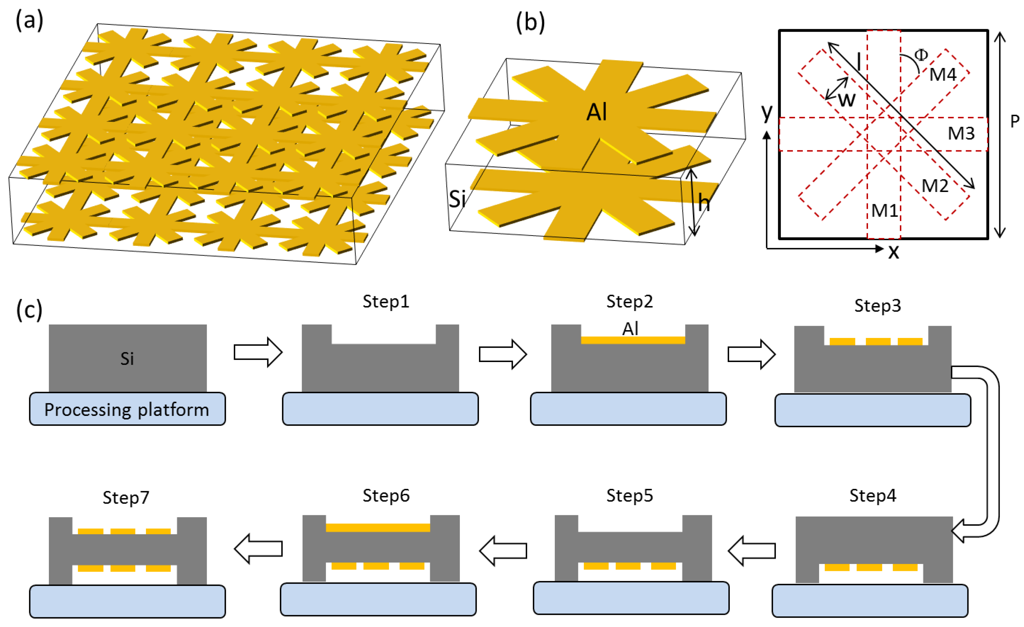
The designed metasurface device structure is shown in Figure 1a. This device is composed of a metal with excellent conductivity (aluminum is used in this work) and high resistance silicon (permittivity ε = 11.9, resistivity ρ > 5000 Ω·cm), presenting a sandwich structure with the same metal pattern on the top and bottom surfaces of the silicon wafer. Each unit cell structure is shown in Figure 1b, with a silicon substrate thickness of h = 100 μm and a metal pattern thickness of 200 nm. The metal pattern is composed of four metal strips of the same size, coded as M1–M4, with an angle of Φ = 45° between adjacent metal strips. The periodic constant of a square cell is P = 300 μm, the length of the metal strip is l = 300 μm, and the width is w = 50 μm. All simulation results were obtained by CST microwave studio software. The simulation process relies on a frequency domain solver, where the “unit cell” boundary conditions are used in the x and y directions, and “open” boundary conditions are used in the z direction.
Although no experimental research is conducted in this work, the proposed structure can be prepared in practice. The recommended preparation scheme is shown in Figure 1c. Using a 200 μm thick silicon wafer as the substrate, first etch one surface of the wafer using ICP (Inductively Coupled Plasma) technology to remove 50 μm silicon. It should be noted that the surface of the wafer cannot be completely etched off, and sufficient area needs to be retained to facilitate subsequent process operations (Step 1). Then, aluminum (Al) film 200 nm thick is deposited on the surface of the etched wafer using thermal evaporation technology (Step 2), and a mature photolithography process is used to etch the pinwheel-shaped metal pattern (Step 3), forming a surface pattern of the sample. The next step is to prepare another surface pattern of the sample. This is shown in Step 4, which requires flipping the sample and using the pre-reserved wafer area (the part of the wafer that has not been etched with ICP in Step 1) as support, where the already-made metal patterns will not be damaged because they do not directly contact the processing platform. At this time, repeat the above steps, first using ICP technology to etch the surface of the silicon wafer to remove 50 μm silicon (remaining a silicon wafer with 100 μm thickness), and then using mature metal vapor deposition and photolithography techniques to prepare a 200 nm thick pinwheel-shaped metal pattern on the etched wafer surface (Step 5–7), ultimately forming a sample with a metal–silicon–metal structure.

3. Results and Discussion

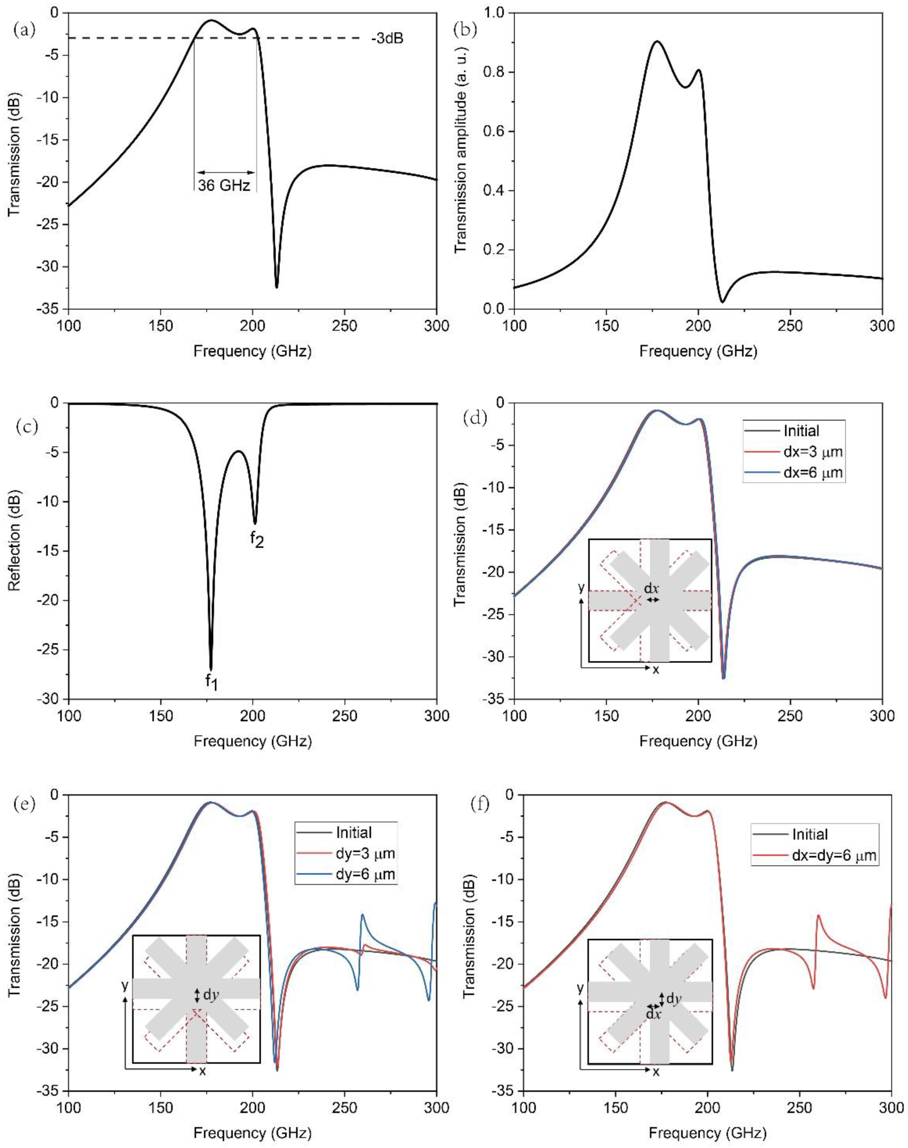
The operating frequency of the device is located in the terahertz band that can serve 6G communication. The incident wave is TE mode, and the transmission and reflection spectra in the vertical incidence are shown in Figure 2. In this work, when a terahertz wave is incident vertically, the TE mode corresponds to y-polarization. The transmission characteristics of the device in the range of 100–300 GHz (0.1–0.3 THz) are shown in Figure 2a,b. It is easy to know from the symmetry of the device that the same results as Figure 2 can be obtained when an x-polarized terahertz wave is incident vertically on the device. It is usually defined that the filtering function is effective when the attenuation of the transmission amplitude of the filter does not exceed 3 dB. From Figure 2a, it can be observed that the bandwidth of the transmission attenuation with 3 dB is 36 GHz, and the effective operating range of the filter is 167–203 GHz. The linear transmission amplitude spectrum corresponds to Figure 2b, and a maximum transmission amplitude of 0.9 can be found. The bandpass filtering is formed by the interaction of two resonances located in close proximity. By detecting the reflection spectrum, the central frequencies of the two resonances can be clearly seen, as shown in Figure 2c. The two resonances are f1 = 175 GHz and f2 = 200 GHz, respectively. In actual manufacture, the structural parameters may not be accurate, so the robustness of the device needs to be considered. The scattering performances may be changed with the disturbances in substrate thickness, metal size, and pattern offset on the opposite sides of the substrate. The variation in substrate thickness and metal size can be controlled very precisely during the manufacturing process (the effects of substrate thickness and metal size will be presented in subsequent discussions.). In contrast, the pattern offset on the opposite sides of the substrate is almost unavoidable and hard to control. Hence, we mainly discuss the pattern offset effect here. Due to the fact that the mask used in the actual manufacturing process is the same for patterns on the opposite sides of the substrate, the patterns can only undergo overall deviation. The offsets along the x and y directions are analyzed, as shown in Figure 2d–f. It can be seen that when the patterns on the opposite sides of the substrate produce a relative dislocation with dx = 6 μm along the x direction (Figure 2d), as well as a relative dislocation with dy = 6 μm along the y direction (Figure 2e), the transmission spectra remain generally unchanged in the range of 100–250 GHz, even if these offsets are as high as 6 μm in both the x and y directions (Figure 2f), which proves the great robustness of the structure.
The reflection amplitude of the second resonance f2 is stronger than that of the first resonance f1, and the reason for this result can be identified through the distribution of electric field and surface current. As shown in Figure 3a, the surface current motion modes of the two resonances are the same, with the current flowing back and forth along the metal strip, which is a characteristic of dipole resonance. The surface current intensity and electric field distribution intensity both indicate that the resonance radiation of f2 is stronger than that of f1, so the reflection amplitude at f2 in the reflection spectrum is higher than that at f1. From the distribution of electric field amplitude at the cross-section of the device shown in Figure 3b, it can be seen that the transmitted electric field at the output port for f1 resonance is stronger than that at the output port for f2 resonance, which is consistent with the transmission and reflection intensity trends of the two resonances shown in Figure 2.
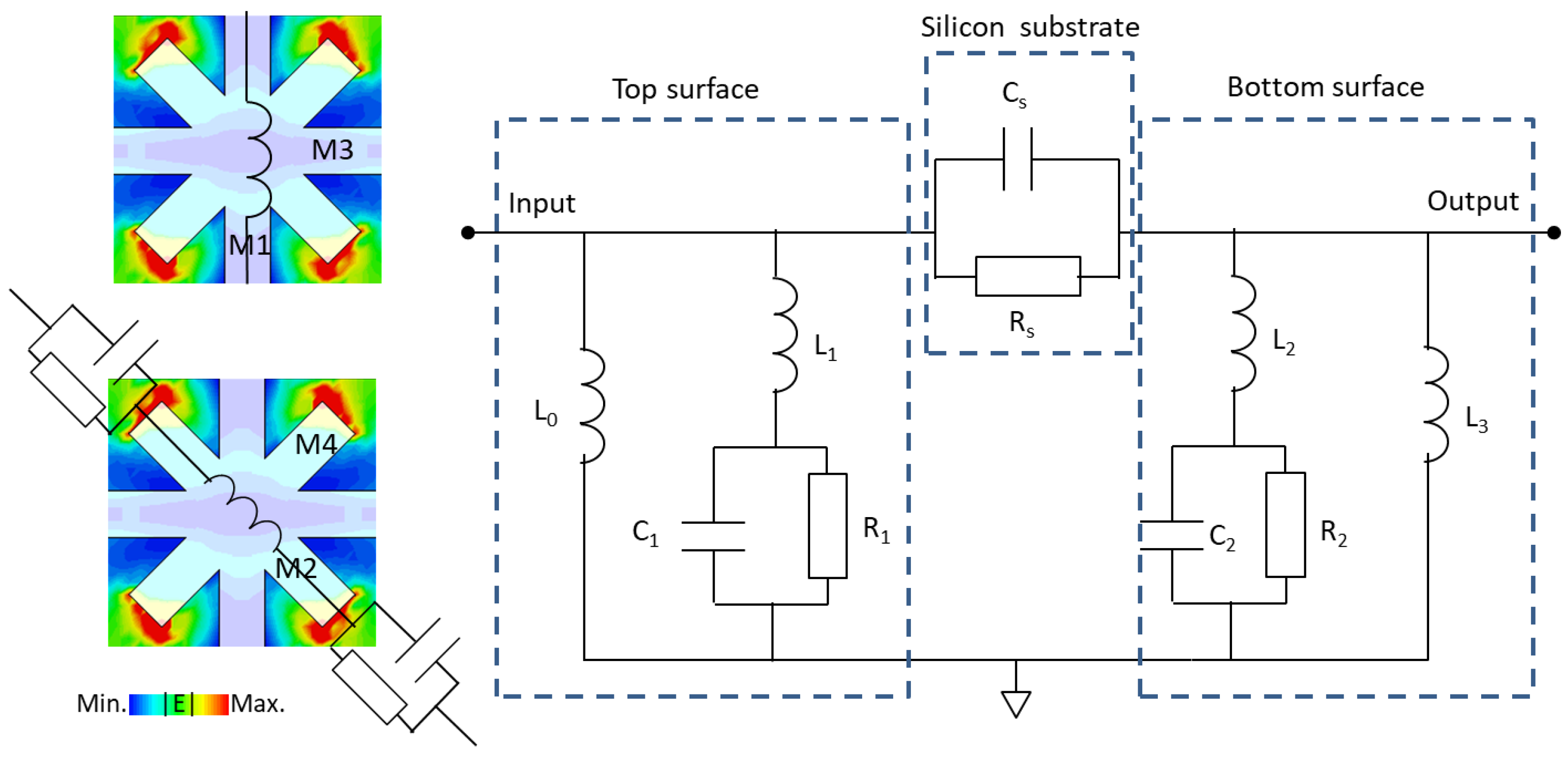
Next, we need to consider an issue as to why the designed metasurface can generate two resonances f1 and f2; in other words, how to explain the formation of these two resonances. To clarify the formation mechanism of two resonances, we use an equivalent circuit model, as shown in Figure 4. The interaction between the incident alternating electric field and the metasurface generates various parasitic electrical effects. The metal strip itself has weak inductance (negligible self-resistance), and under the excitation of an external electric field, non-metallic media will also produce resistance and capacitive effects. The metal strips M1 and M3 on the surface of the unit cell can be equivalent to a weak inductance L0, and the metal strips M2 and M4 can be equivalent to a weak inductance L1. There are gaps between M2 and M2 (as well as M4 and M4) of adjacent unit cells, which will generate equivalent capacitance C1 and resistance R1 with a parallel connection. The metal structure on the bottom surface of the silicon substrate is identical to that on the top surface. The metal strips M1 and M3 on the bottom surface are equivalent to L3, while the metal strips M2 and M4 on the bottom surface are equivalent to L2. The gaps between M2 and M2 (as well as M4 and M4) of adjacent unit cells on the bottom surface are equivalent to a parallel connection of C2 and R2. Due to the same size of all metal strips, where L0 = L1 = L2 = L3, R1 = R2, and C1 = C2. The metal structure between the top and bottom of the unit cell is a silicon substrate, which has parasitic capacitance and parasitic resistance. Therefore, it can be equivalent to a capacitor Cs and a resistor Rs in parallel. It can be understood that the RC circuit in Figure 4 carries two resonance frequencies, namely 1/(2πR1C1) and 1/(2πRsCs), respectively.
By analyzing the changes in resonance positions under different structural parameters, we can determine the corresponding relationship between the two resonance frequencies (1/(2πR1C1) and 1/(2πRsCs)) in the RC equivalent circuit of Figure 4 and the two resonance frequencies (f1 and f2) in the reflection spectrum of Figure 2. Firstly, by keeping the structural parameters of the metal strip unchanged and changing the thickness of the silicon substrate, the reflection and transmission spectra of the device are obtained as shown in Figure 5. Due to the constant size of the metal strip structure, both L0–L3, R1–R2, and C1–C2 in Figure 4 remain unchanged, which means that 1/(2πR1C1) remains unchanged. In Figure 5, the resonance located at 200 GHz (corresponding to f2 in Figure 2) does not vary with the thickness of the silicon substrate, indicating that the resonance f2 originates from the metal structure. The values of R1 and C1 are easily estimated: the resistance value R1 ≈ 1 × 10⁶ Ω, which can be calculated by the distance between two tilted metal strips, the thickness of silicon h, and the electrical resistivity ρ; and the capacitance value C1 ≈ 8 × 10⁻¹⁸ F, which can be obtained by the metal strip width w, metal thickness, gap distance, and vacuum permittivity ε0. Thus, f2 = 1/(2πR1C1) ≈ 200 GHz. The other resonance, f1, is controlled by Rs and Cs. As the thickness of the silicon substrate increases, the equivalent capacitance Cs decreases while the equivalent resistance Rs significantly increases, ultimately causing 1/(2πRsCs) to decrease so that f1 shifts toward low frequencies in the spectrum. Unlike f2, the resonance associated with f1 mainly occurs at the top of the tilted metal strip (as can be observed from the localized position of the electric field in Figure 3a), and its resonance area is difficult to accurately calculate, resulting in the high resistance silicon capacitance value covered by the resonance area being difficult to calculate. But the order of magnitude of C2 can still be estimated because the thickness of high resistance silicon is of the same order of magnitude as the gap between tilted metal strips (both in the order of hundreds of micrometers), and the dielectric parameter of silicon relative to vacuum is of the order of 10, so the capacitance value of C2 is about 10−17 F level. In addition, high resistance silicon is sandwiched between the upper and lower metal, with a resistance of about 105 Ω level, which is easily calculated based on the area, thickness, and resistivity of silicon. Therefore, the order of magnitude of f1 = 1/(2πRsCs) is also at the 102 GHz level.
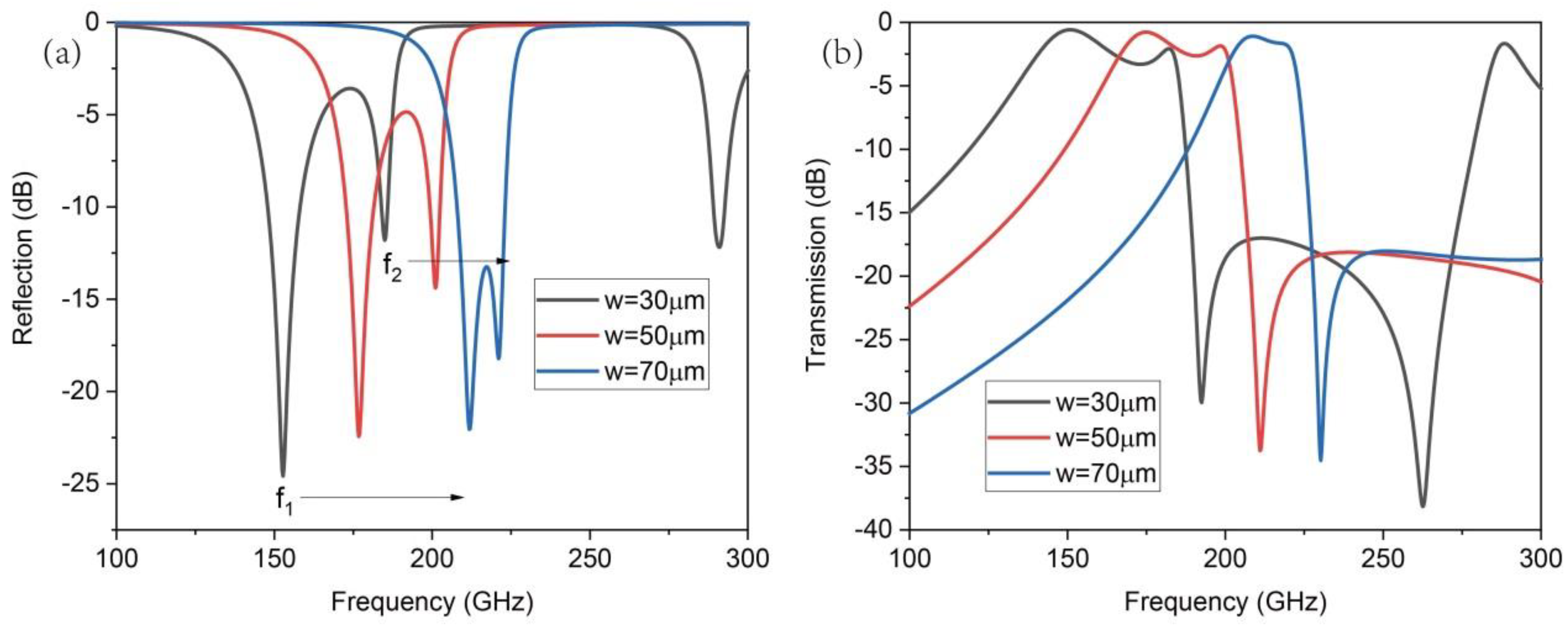
The analysis in Figure 5 shows that resonance f1 is correlated with Rs. Figure 6 shows the reflection and transmission spectra after changing the metal width of the device with constant silicon thickness (h = 100 um). The increasing width of the metal leads to an increase in the metal pattern area, which directly increases the covered silicon area. Therefore, the equivalent resistance Rs of the silicon substrate decreases, resulting in 1/(2πRsCs) increasing; thus, f1 moves toward high frequencies. At the same time, increasing the width of the metal will also lead to a decrease in R1, resulting in 1/(2πR1C1) increasing; thus, f2 also moves toward high frequencies.
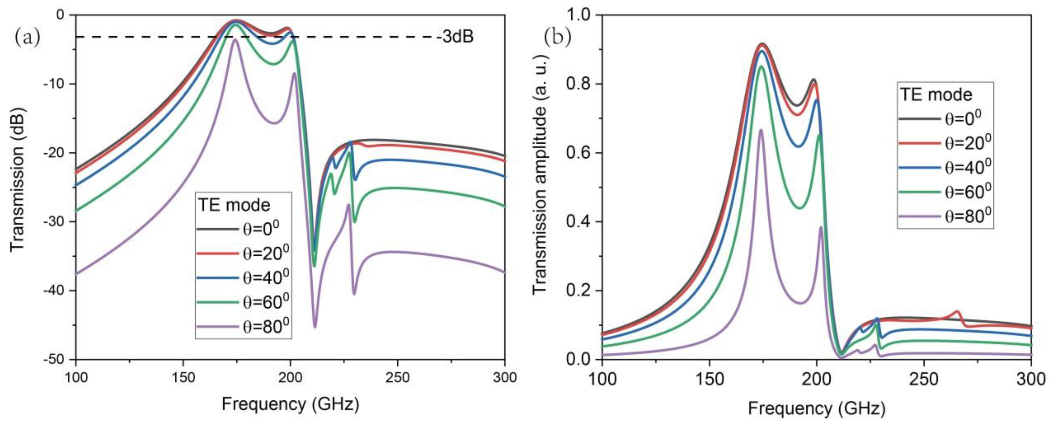
Considering that in practical applications, electromagnetic beams are not completely perpendicular to the device surface, it is necessary to consider the impact of beam incidence angle on the filtering characteristics of the device. The transmission spectra at different incident angles are shown in Figure 7, with the incident wave vector located in the yz plane and the angle between the incident wave and the z-axis normal in the yz plane being θ. It can be seen that the two resonance centers located at 175 GHz and 200 GHz do not change with the change in incident angle, while the resonance amplitude depends on the incident angle. When the incident angle θ does not exceed 20°, the device can maintain a similar operating bandwidth and transmission amplitude as in the case of vertical incidence.
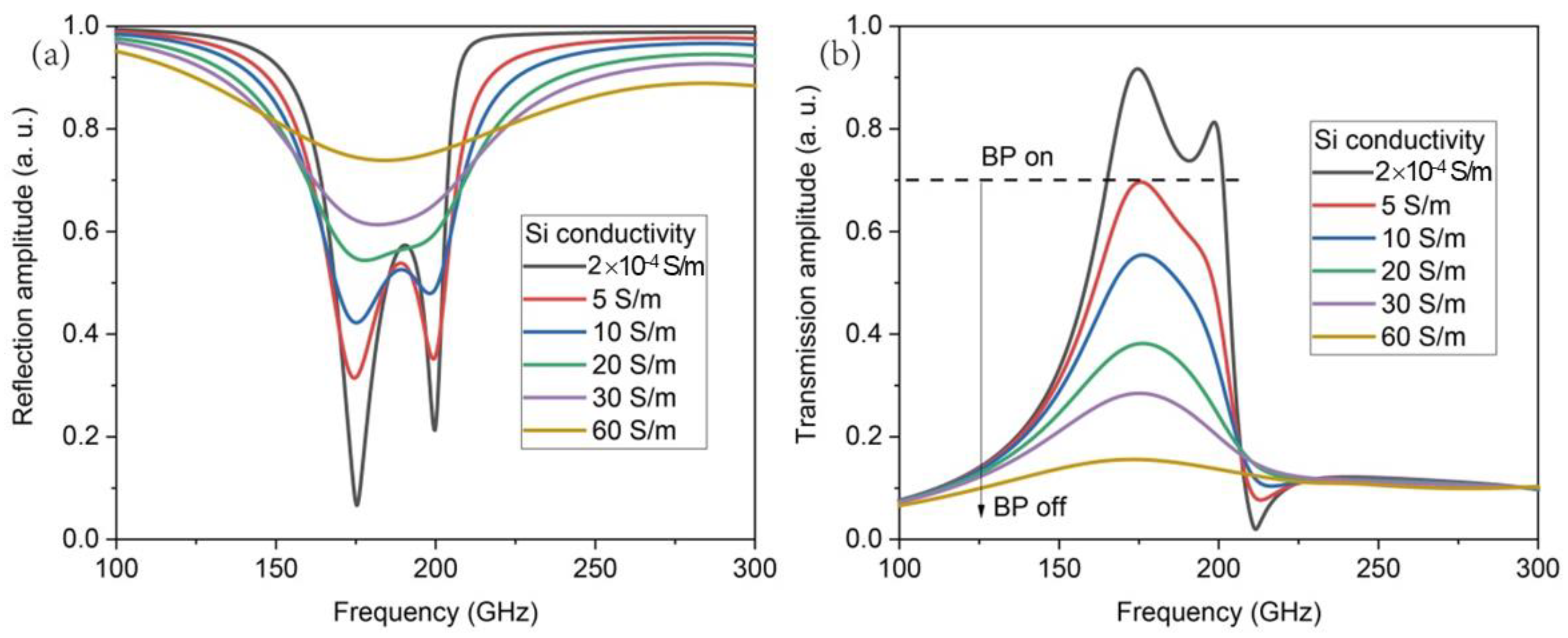
The carrier concentration of silicon medium can be changed under external light excitation (it is necessary that the photon energy of excitation light is greater than the energy gap of silicon), resulting in variable resonance intensity [21]. This property enables this device to have filtering and switching characteristics. Exciting light can be achieved by selecting a continuous wave with a wavelength of 1064 nm. Previous studies have shown that high resistance silicon can absorb light with a wavelength of 1064 nm, and 1064 nm light can penetrate a high resistance silicon with at least 500 μm thickness [21]. The silicon thickness used in this work is only 100 μm, which means that carriers in the entire silicon can be excited by 1064 nm light. Experiments have shown that when the power of a 1064 nm continuous wave reaches several mW, the conductivity of high resistance silicon can reach tens of S/m [21]. Therefore, it is reasonable for this work to simulate the influence of light excitation on the performance of the device by changing the silicon conductivity. The results of the reflection and transmission spectra of the device, accompanied by changes in silicon conductivity, are shown in Figure 8. When the conductivity of silicon transitions from a high resistance state to a low resistance state, terahertz resonance weakens, and the reflection of terahertz waves by silicon is significantly enhanced, mainly due to an increase in carriers on the silicon surface. Correspondingly, the transmission amplitude of the device is significantly reduced. When the conductivity of silicon increases from 2 × 10⁻⁴ S/m to 60 S/m, the maximum transmission amplitude decreases from 0.9 to 0.1, meaning that the bandpass filtering characteristics of the device are turned off.
4. Conclusions

This work is aimed at space terahertz communication applications, and a terahertz bandpass filter has been designed using highly conductive metals and high resistance silicon. The filter is a metasurface device with a sandwich structure, and the basic unit cell configuration is a double-layer pinwheel-shaped metal structure mixed with a silicon substrate. The bandwidth of the transmission amplitude attenuation of 3 dB is 36 GHz, and the effective operating range of the filter is 167–203 GHz. The maximum transmission amplitude can reach 0.9, and these characteristics can be maintained within an incident beam angle of 20°. This work uses an equivalent RC resonant circuit to explain the formation of bandpass filtering, and it is found that the bandpass filter originates from the interaction between two close resonances. Furthermore, in order to enhance the controllability of the bandpass filtering function of the device, the photosensitive characteristics of silicon can be used to modify the carrier concentration of silicon, thereby affecting the resonance intensity and ultimately enabling the device to have filtering and switching characteristics under light excitation.

Author Contributions

W.L.: Conceptualization, methodology, and writing the original manuscript. J.L.: Conceptualization, Data curation, software, and reviewing. All authors have read and agreed to the published version of the manuscript.

Funding

This research received no external funding.

Institutional Review Board Statement

Not applicable.

Informed Consent Statement

Not applicable.

Data Availability Statement

The data that support the findings of this study are available from the corresponding author upon reasonable request.

Conflicts of Interest

Author Wenjun Liu was employed by the Chengdu Huanyuxin Technology Co., Ltd. The remaining authors declare that the research was conducted in the absence of any commercial or financial relationships that could be construed as a potential conflict of interest.

References

  1. Rogalski, A.; Sizov, F. Terahertz detectors and focal plane arrays. Opto-Electron. Rev. 2011, 19, 346–404. [Google Scholar] [CrossRef]
  2. Huang, Y.; Yang, R.; Xiao, T.; Li, H.; Tian, M.; Xie, Z.; Zheng, J.; Zhu, J.; Su, Y.; Chen, W.; et al. Wafer-scale self-assembled 2.5D metasurface for efficient near-field and far-field electromagnetic manipulation. Appl. Surf. Sci. 2022, 601, 154244. [Google Scholar] [CrossRef]
  3. Wu, P.C.; Tsai, W.-Y.; Chen, W.T.; Huang, Y.-W.; Chen, T.-Y.; Chen, J.-W.; Liao, C.Y.; Chu, C.H.; Sun, G.; Tsai, D.P. Versatile Polarization Generation with an Aluminum Plasmonic Metasurface. Nano Lett. 2017, 17, 445–452. [Google Scholar] [CrossRef]
  4. Gao, Y.-J.; Xiong, X.; Wang, Z.; Chen, F.; Peng, R.-W.; Wang, M. Simultaneous Generation of Arbitrary Assembly of Polarization States with Geometrical-Scaling-Induced Phase Modulation. Phys. Rev. X 2020, 10, 031035. [Google Scholar] [CrossRef]
  5. Wang, S.; Deng, Z.-L.; Wang, Y.; Zhou, Q.; Wang, X.; Cao, Y.; Guan, B.-O.; Xiao, S.; Li, X. Arbitrary polarization conversion dichroism metasurfaces for all-in-one full Poincaré sphere polarizers. Light Sci. Appl. 2021, 10, 24. [Google Scholar] [CrossRef] [PubMed]
  6. Huang, Y.; Xiao, T.; Xie, Z.; Zheng, J.; Su, Y.; Chen, W.; Liu, K.; Tang, M.; Zhu, J.; Müller-Buschbaum, P.; et al. Multistate nonvolatile metamirrors with tunable optical chirality. ACS Appl. Mater. Interfaces 2021, 13, 45890–45897. [Google Scholar] [CrossRef]
  7. Huang, Y.J.; Xiao, T.X.; Chen, S.; Xie, Z.W.; Zheng, J.; Zhu, J.; Su, Y.; Chen, W.; Liu, K.; Tang, M.; et al. All-optical controlled-NOT logic gate achieving directional asymmetric transmission based on metasurface doublet. Opto-Electron. Adv. 2023, 6, 220073. [Google Scholar] [CrossRef]
  8. Balli, F.; Sultan, M.; Lami, S.K.; Hastings, J.T. A hybrid achromatic metalens. Nat. Commun. 2020, 11, 3892. [Google Scholar] [CrossRef] [PubMed]
  9. Zheng, C.; Li, J.; Yue, Z.; Li, J.; Liu, J.; Wang, G.; Wang, S.; Zhang, Y.; Zhang, Y.; Yao, J. All-dielectric trifunctional metasurface capable of independent amplitude and phase modulation. Laser Photonics Rev. 2022, 16, 2200051. [Google Scholar] [CrossRef]
  10. Li, J.; Liu, J.; Yue, Z.; Li, J.; Zheng, C.; Yang, F.; Li, H.; Zhang, Y.; Zhang, Y.; Yao, J. Polarization variable terahertz metasurface along the propagation path. Fundam. Res. 2023. [Google Scholar] [CrossRef]
  11. Rubin, N.A.; D’Aversa, G.; Chevalier, P.; Chevalier, P.; Shi, Z.; Chen, W.T.; Capasso, F. Matrix Fourier optics enables a compact full-Stokes polarization camera. Science 2019, 365, eaax1839. [Google Scholar] [CrossRef] [PubMed]
  12. Jiang, Z.H.; Kang, L.; Yue, T.; Xu, H.; Yang, Y.; Jin, Z.; Yu, C.; Hong, W.; Werner, D.H.; Qiu, C. A Single Noninterleaved Metasurface for High-Capacity and Flexible Mode Multiplexing of Higher-Order Poincaré Sphere Beams. Adv. Mater. 2020, 32, 1903983. [Google Scholar] [CrossRef] [PubMed]
  13. Cao, G.; Xu, H.-X.; Zhou, L.-M.; Deng, Y.; Zeng, Y.; Dong, S.; Zhang, Q.; Li, Y.; Yang, H.; Song, Q.; et al. Infrared metasurface-enabled compact polarization nanodevices. Mater. Today 2021, 50, 499–515. [Google Scholar] [CrossRef]
  14. Jin, Z.; Janoschka, D.; Deng, J.; Ge, L.; Dreher, P.; Frank, B.; Hu, G.; Ni, J.; Yang, Y.; Li, J.; et al. Phyllotaxis-inspired nanosieves with multiplexed orbital angular momentum. eLight 2021, 1, 5. [Google Scholar] [CrossRef]
  15. Zentgraf, T. Imaging the rainbow. Nat. Nanotechnol. 2018, 13, 179–180. [Google Scholar] [CrossRef] [PubMed]
  16. Cambiasso, J.; König, M.; Cortes, E.; Schlücker, S.; Maier, S.A. Surface-enhanced spectroscopies of a molecular monolayer in an all-dielectric nanoantenna. ACS Photonics 2018, 5, 1546–1557. [Google Scholar] [CrossRef]
  17. Romano, S.; Zito, G.; Managò, S. Surface-enhanced Raman and fluorescence spectroscopy with an all-dielectric metasurface. J. Phys. Chem. C 2018, 122, 19738–19745. [Google Scholar] [CrossRef]
  18. Zhao, Y.-T.; Zhang, J.-J.; Wu, B. Low Profile Reflective Polarization Conversion Metasurface with High Frequency Selectivity. IEEE Trans. Antennas Propag. 2022, 70, 10614–10622. [Google Scholar] [CrossRef]
  19. Lalbakhsh, A.; Afzal, M.U.; Esselle, K.P.; Smith, S.L. All-Metal Wideband Frequency-Selective Surface Bandpass Filter for TE and TM Polarizations. IEEE Trans. Antennas Propag. 2022, 70, 2790–2800. [Google Scholar] [CrossRef]
  20. Darvish, A.; Kish, A.A. X-Band Nearfield Shielding Metasurface With Adjustable Reflection/Transmission Zeroes. IEEE Trans. Electromagn. Compat. 2022, 64, 1602–1613. [Google Scholar] [CrossRef]
  21. Li, J.; Li, J.; Zheng, C.; Yue, Z.; Yang, D.; Wang, S.; Li, M.; Zhang, Y.; Yao, J. Spectral amplitude modulation and dynamic near-field displaying of all-silicon terahertz metasurfaces supporting bound states in the continuum. Appl. Phys. Lett. 2021, 119, 241105. [Google Scholar] [CrossRef]
Figure 1. (a) Schematic diagram of the designed metasurface device structure. (b) 3D and 2D views of a unit cell. (c) The suggested sample processing techniques. Step 1: Etch to remove 50 μm silicon; Step 2: Deposit a 200 nm Al film; Step 3: Photolithography to form a metal pattern; Step 4: Flip the sample and repeat Steps 1 to Step 3 (corresponding to Steps 5 to Step 7).
Photonics 11 00559 g001
Figure 2. (a,b) show the transmission spectrum of TE mode at normal incidence with (a) dB scale and (b) linear scale, respectively. Correspondingly, (c) shows the reflection spectrum with dB scale, where f1 = 175 GHz and f2 = 200 GHz. (d,e,f) shows the transmission spectra with dB scale for pattern offsets (d) along the x direction, (e) along the y direction, and (f) along diagonal line. The inserts in (d,e,f) shows the relative position for patterns on the opposite sides of the substrate, in which the red dotted line graphic represents the structure at the initial position, while the grey-filled graphic represents the offset pattern.
Photonics 11 00559 g002
Figure 3. (a) Surface current and electric field amplitude distribution of two resonances f1 and f2, corresponding (b) cross-sectional electric field amplitude distribution.
Photonics 11 00559 g003
Figure 4. The equivalent RC resonance circuit model of metasurface resonances. The R1 and C1 are 106 Ω and 10−18 F level, respectively. The Rs and Cs are 105 Ω and 10−17 F level, respectively.
Photonics 11 00559 g004
Figure 5. The (a) reflection and (b) transmission characteristics of devices follow the trend of changes in silicon substrate thickness while maintaining the size of the metal structure unchanged.
Photonics 11 00559 g005
Figure 6. The (a) reflection and (b) transmission characteristics of the device follow the trend of changing the width of the metal strip, keeping the silicon thickness unchanged.
Photonics 11 00559 g006
Figure 7. The transmission spectrum of the device under different scanning angles: (a) In dB units; (b) In linear units.
Photonics 11 00559 g007
Figure 8. The (a) reflection and (b) transmission spectra of devices with different silicon conductivity, where terahertz waves are incident vertically.
Photonics 11 00559 g008
Disclaimer/Publisher’s Note: The statements, opinions and data contained in all publications are solely those of the individual author(s) and contributor(s) and not of MDPI and/or the editor(s). MDPI and/or the editor(s) disclaim responsibility for any injury to people or property resulting from any ideas, methods, instructions or products referred to in the content.