A Review of Light-Emitting Diodes and Ultraviolet Light-Emitting Diodes and Their Applications


Abstract
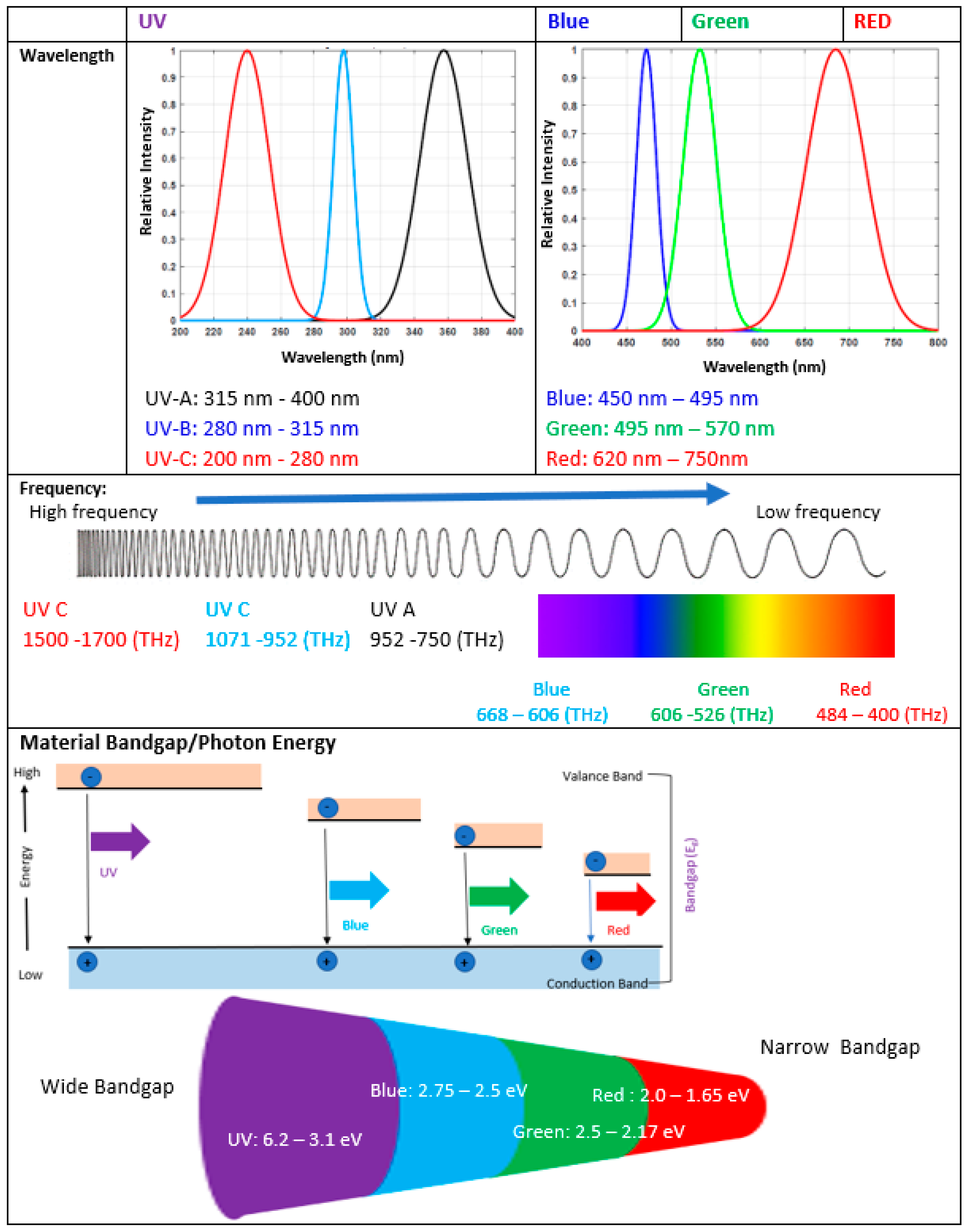
1. Introduction

| UV | Blue | Green | Red | |
|---|---|---|---|---|
| Growth Method | ||||
| Group-Combination (II, III, V, VI) |
|
| ||
| Type of Junctions Used in fabrication |
2. Evolutionary History of LEDs
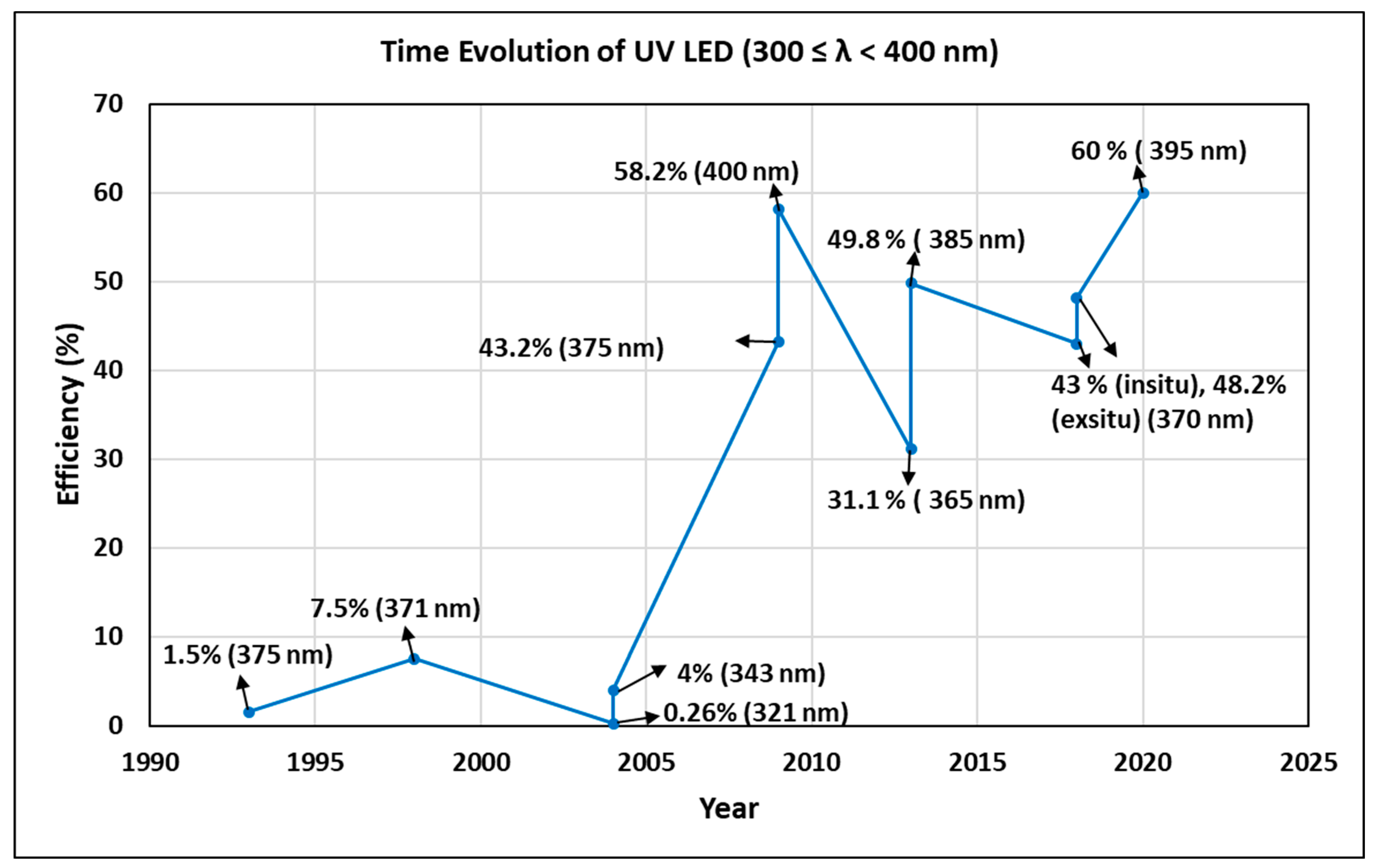
2.1. Evolution of UV LEDs
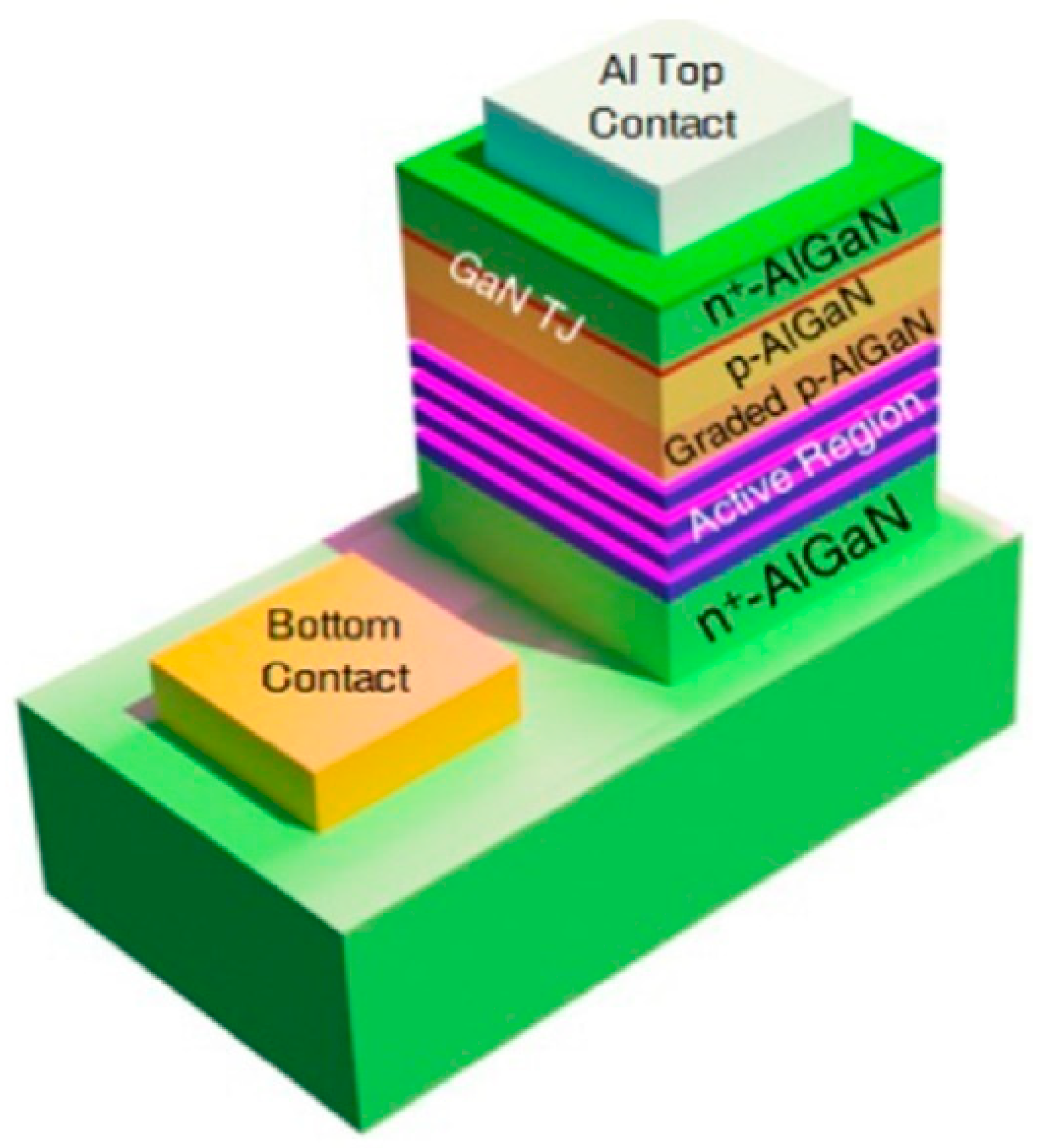
2.1.1. UV—Wavelengths Longer than 300 nm
2.1.2. UV—Wavelength Shorter than 300 nm
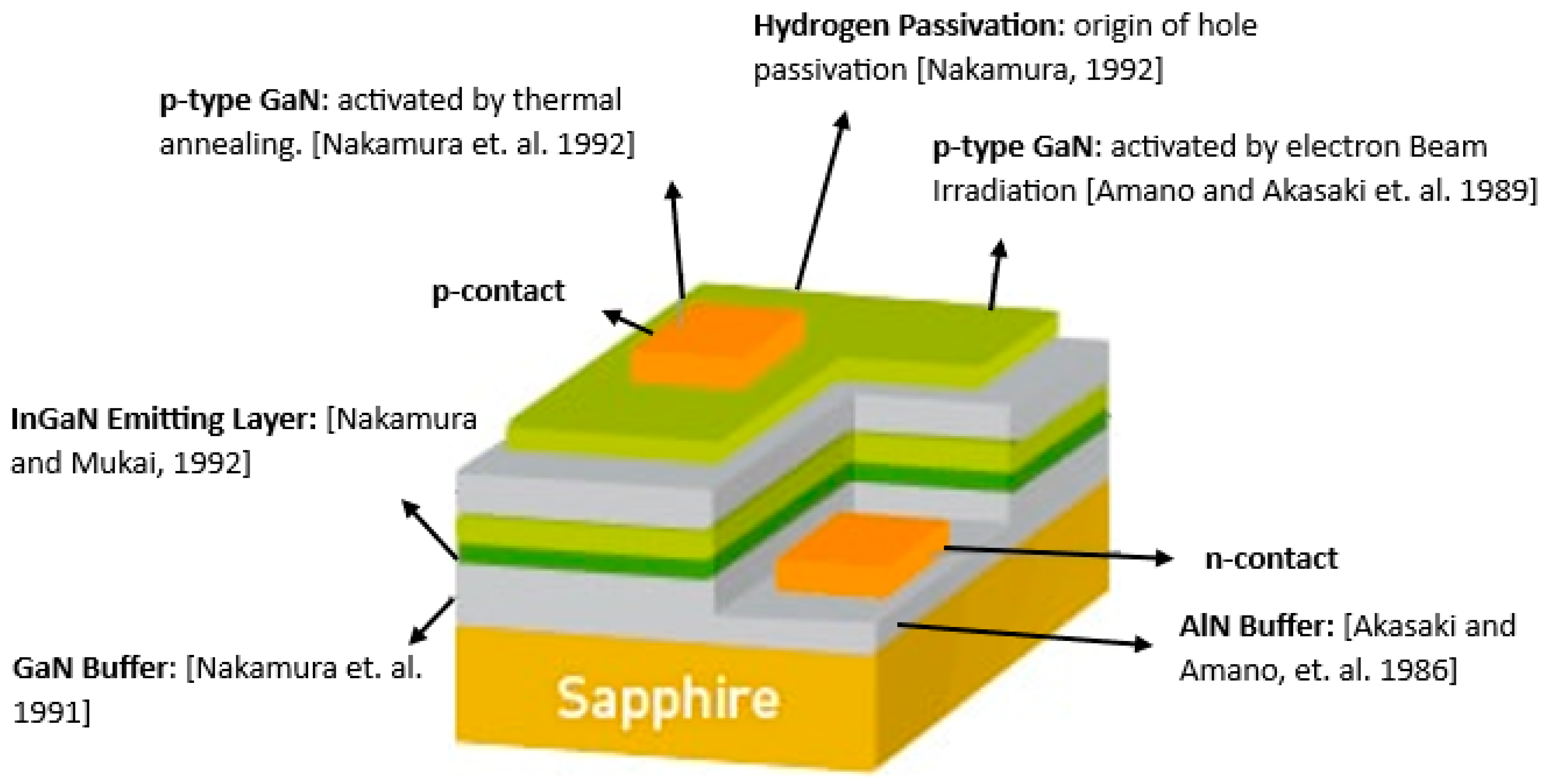
2.2. Evolution of Blue LED

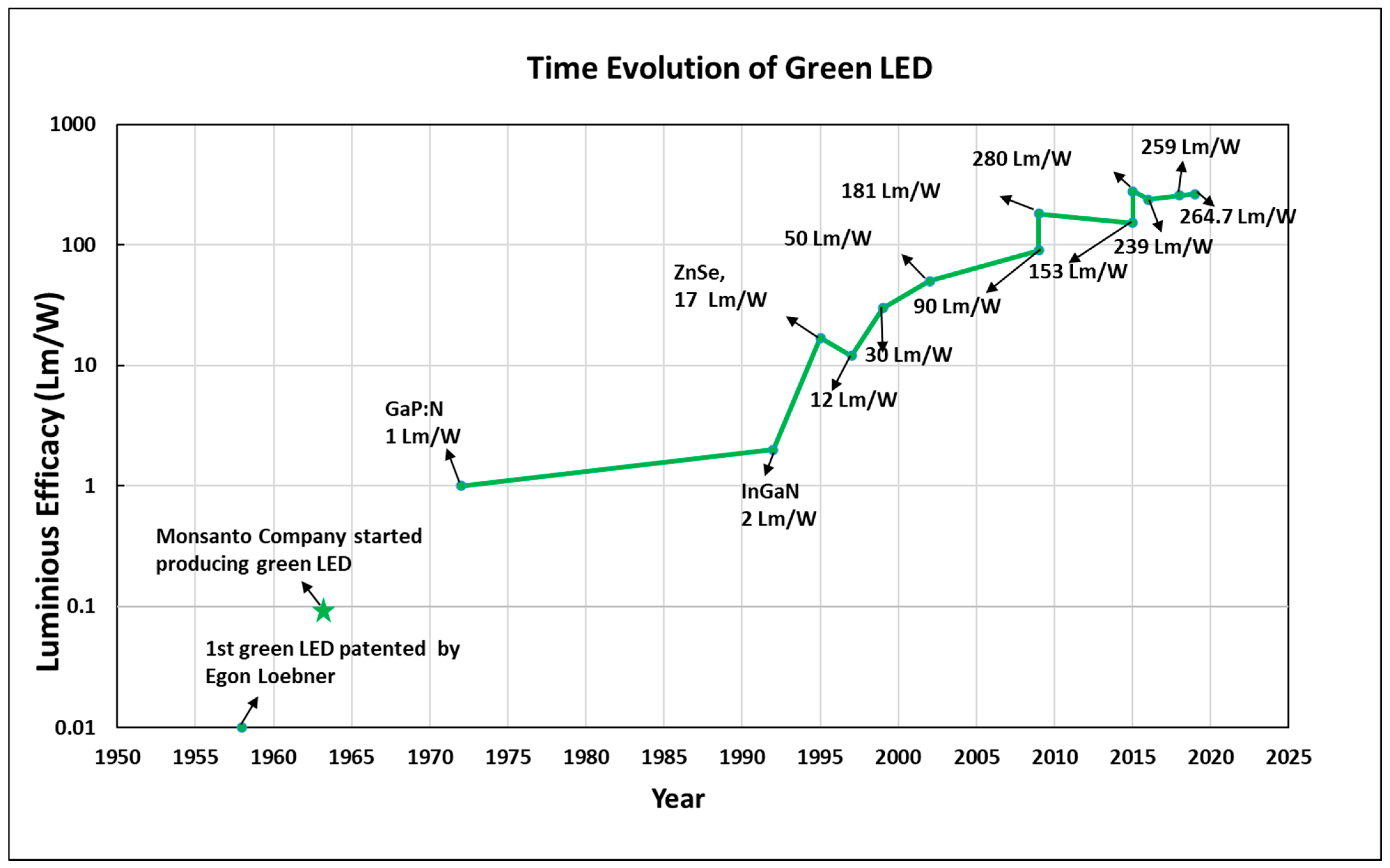
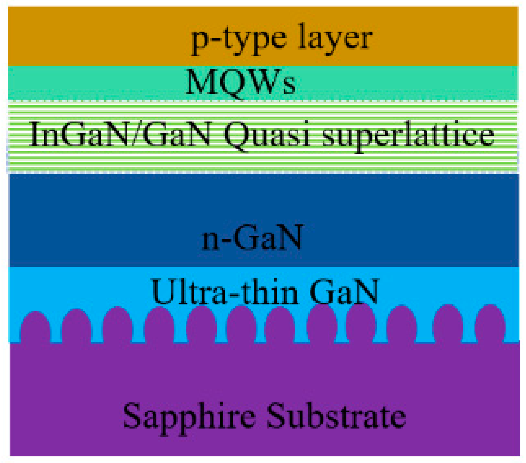
2.3. Evolution of Green LED
2.4. Evolution of Red LEDs
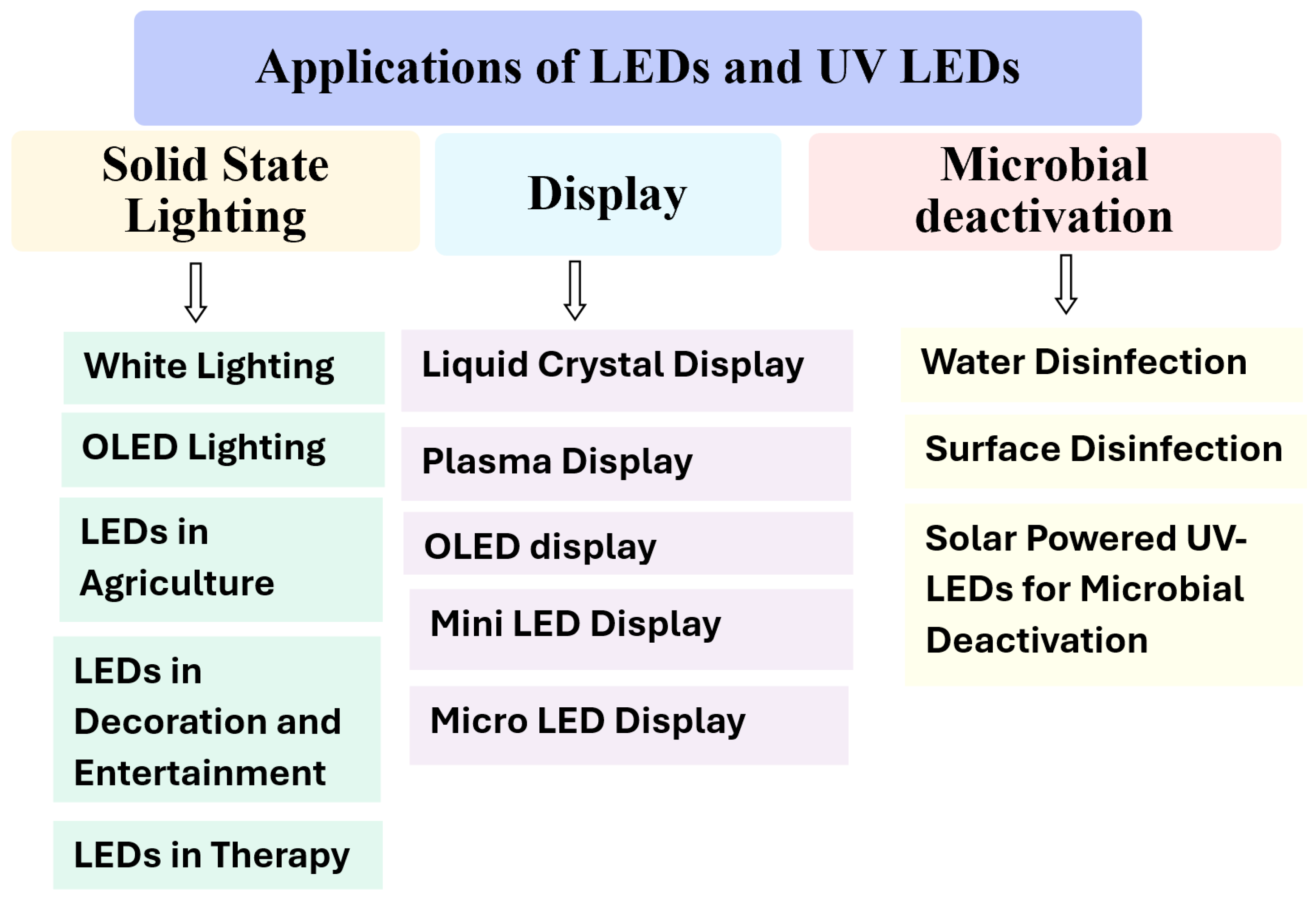
3. Prospects of LED Lighting Technology
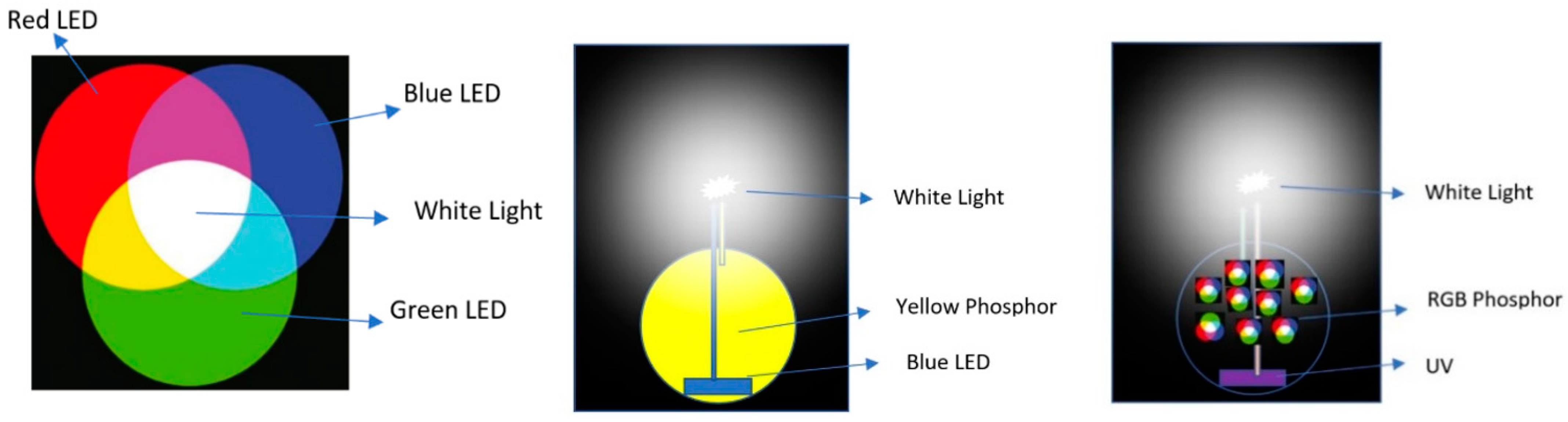
3.1. Application of LED in White Lighting
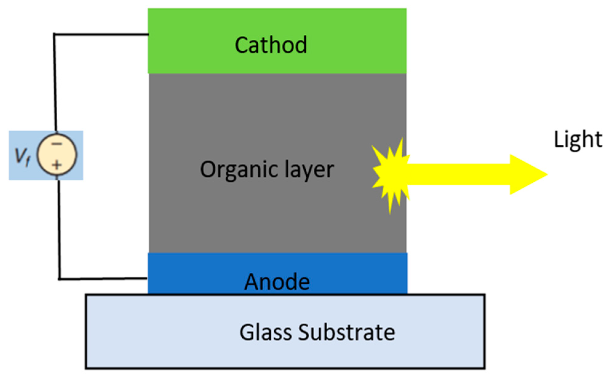
3.2. OLED Lighting
3.3. LED Lighting in Agriculture
3.4. LED Lighting in Decoration and Entertainment
3.5. LED Lighting in Therapy
4. Applications of LEDs in Display Technology
4.1. Liquid Crystal Displays (LCDs)
4.2. Plasma Display
4.3. OLED Displays
4.4. Mini-LED (mLED) Displays
4.5. Micro-LED (µLED) Displays
5. Applications of LEDs in Disinfection of Microbes
5.1. Application of UV-LEDs in Water Purification
5.2. Application of UV LEDs in Microbial Disinfection from Surfaces
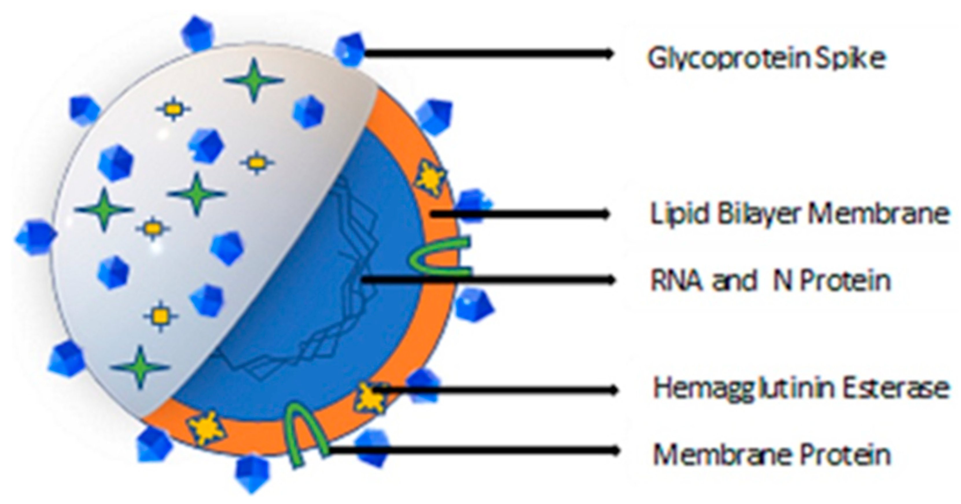

5.2.1. Coronavirus Types
5.2.2. Microorganism Response to UV Radiation
| Viruses | Wavelength (nm) | Sample Condition | UV Dose for log Reduction (mJ/cm2) | References |
|---|---|---|---|---|
| HCoV-229E (alpha coronavirus | 222 | Aerosol | 0.56 | [206] |
| OC43 (beta coronavirus) | 222 | Aerosol | 0.39 | [206] |
| MERS-CoV | 254 | Droplets | No dose information but successfully deactivated | [207] |
| HCoV-229E | 254 | Liquid serum cell culture | No dose information but successfully deactivated | [207] |
| HCoV-OC43 | 254 | Liquid serum cell culture | No dose information but successfully deactivated | [208] |
| SARS-CoV Hanoi | 254 | Liquid serum cell culture | 22.67 | [209] |
| HCoV-OC43 | 267 | Vero E6 cells | 6.8 (for 4-log reduction) | [210] |
| HCoV-OC43 | 279 | Vero E6 cells | 8.7 (for 4-log reduction) | [210] |
| SARS-CoV | 254 | Salt solution | No dose information but successfully deactivated | [211] |
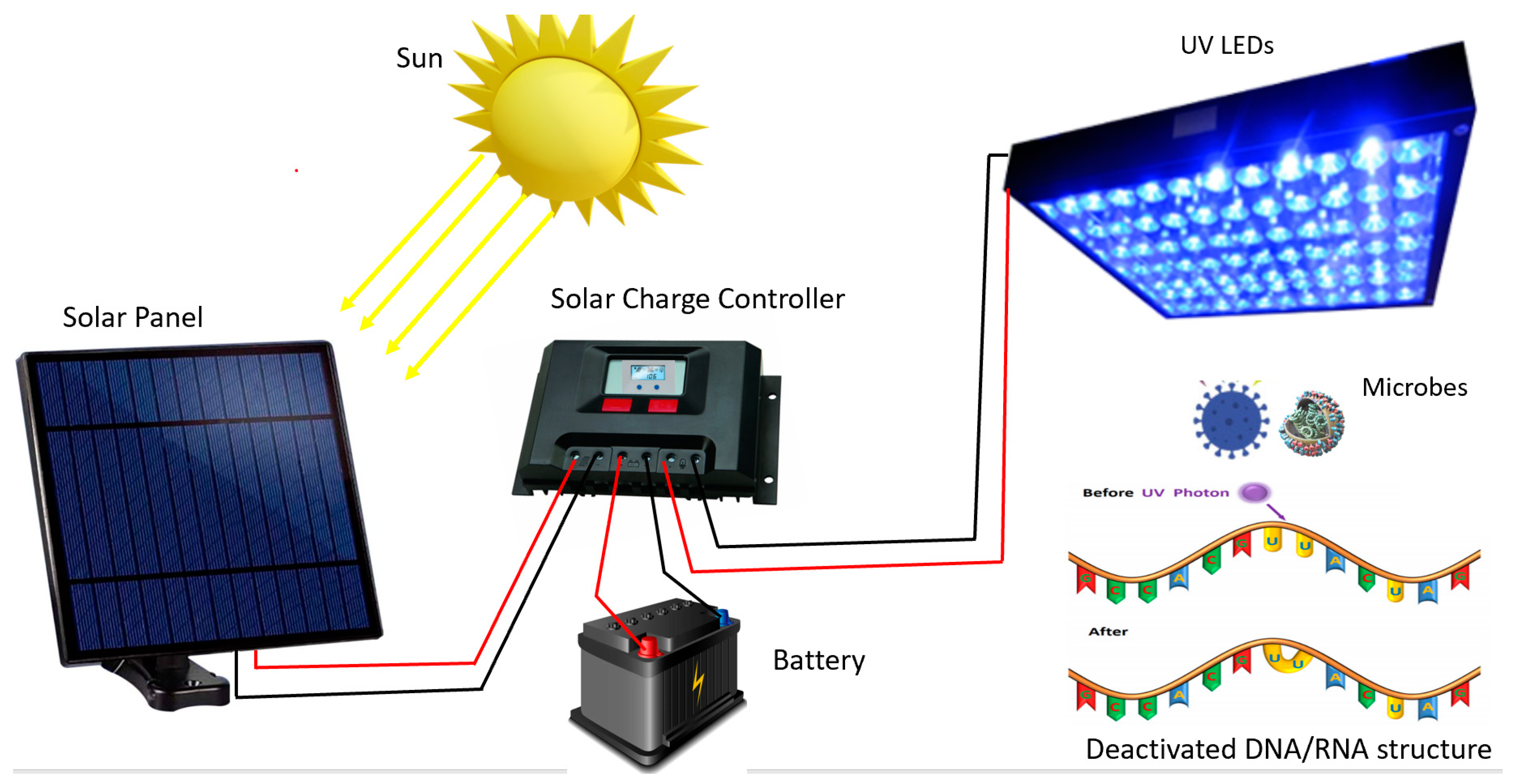
6. The Future in Designing a UV LED Disinfection System
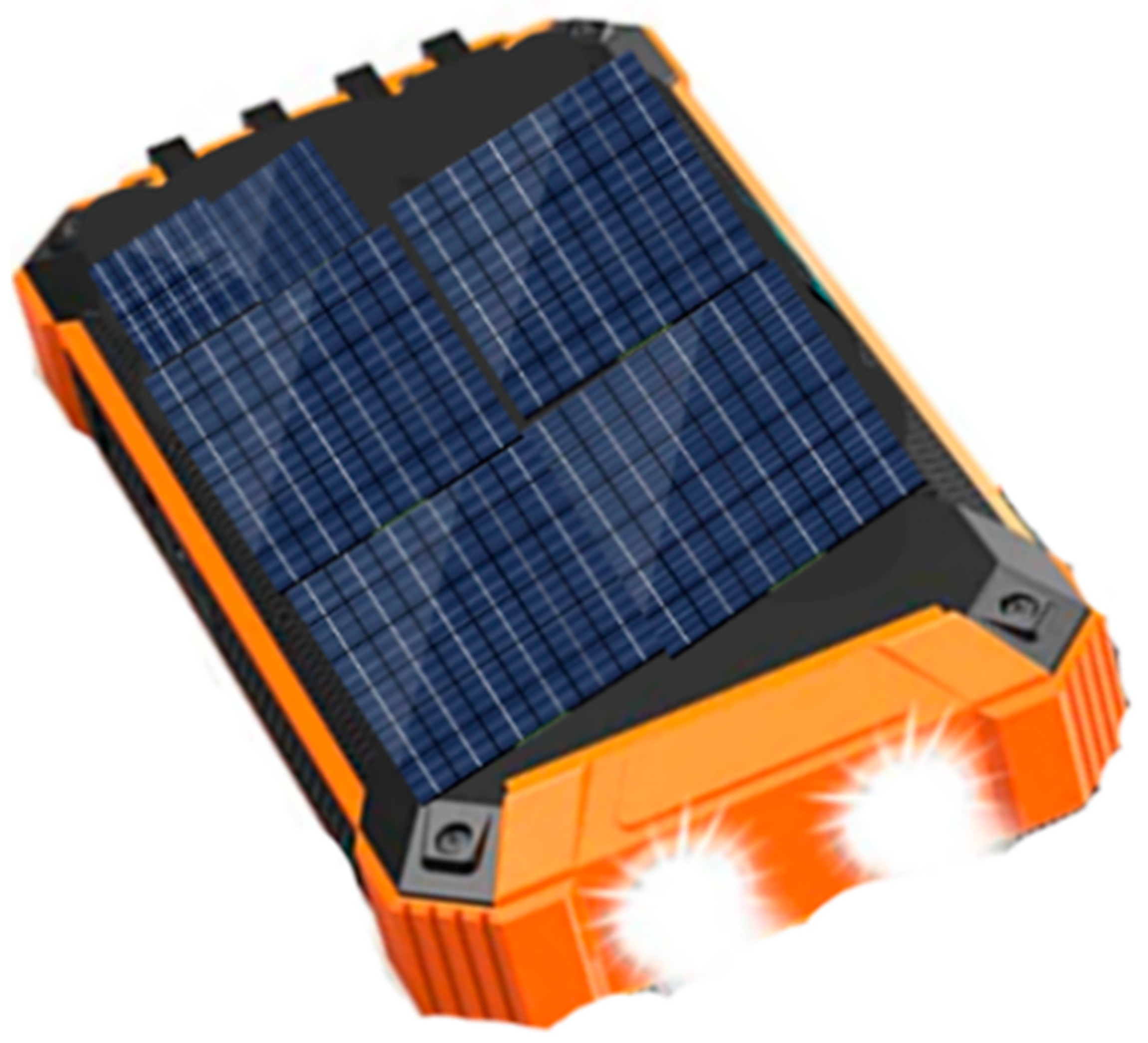
6.1. Building a Deactivation System for Wealthy and Underprivileged Populations with PV Power
6.2. Manufacturing of Cost-Effective Portable High-Precision Virus Deactivation System
7. Discussion and Conclusions
Author Contributions
Funding
Data Availability Statement
Conflicts of Interest
References
- Lu, X.; Hua, T.; Wang, Y. Thermal analysis of high-power LED package with heat pipe heat sink Heat pipe. Microelectron. J. 2011, 42, 1257–1262. [Google Scholar] [CrossRef]
- Novikov, M.A. Oleg Vladimirovich Losev: Pioneer of semiconductor electronics (celebrating one hundred years since his birth). Phys. Solid State 2004, 46, 1–4. [Google Scholar] [CrossRef]
- Yurchuk, S.; Rabinovich, O.; Didenko, S. LED and Phototransistor Simulation. In Optoelectronics-Advanced Device Structures; Pyshkin, S., Ballato, J., Eds.; IntechOpen: Rijeka, Croatia, 2017; pp. 50–51. [Google Scholar]
- Phillips, J.; Coltrin, M.; Crawford, M.; Fischer, A.; Krames, M.; Mueller-Mach, R.; Mueller, G.; Ohno, Y.; Rohwer, L.; Simmons, J.; et al. Research challenges to ultra-efficient inorganic solid-state lighting. Laser Photon. Rev. 2007, 1, 307–333. [Google Scholar] [CrossRef]
- Weisbuch, C. On the search for efficient solid state light emitters: Past, present, future. ECS J. Solid State Sci. Technol. 2020, 9, 016022. [Google Scholar] [CrossRef]
- Rahman, F. Solid-state lighting with wide bandgap semiconductors. MRS Energy Sustain. 2014, 1, E6. [Google Scholar] [CrossRef]
- Maraj, M.; Min, L.; Sun, W. Reliability analysis of AlGaN-based deep UV-LEDs. Nanomaterials 2022, 12, 3731. [Google Scholar] [CrossRef] [PubMed]
- Chayed, N.F.; Badar, N.; Rusdi, R.; Kamarudin, N.; Kamarulzaman, N. Optical bandgap energies of magnesium oxide (MgO) thin film and spherical nanostructures. AIP Conf. Proc. 2011, 1400, 328–332. [Google Scholar]
- Li, S.; Chen, H.; Wang, W.; Yao, D.; Xia, Y.; Zeng, Y. Effects of Y2O3 /MgO ratio on mechanical properties and thermal conductivity of silicon nitride ceramics. Int. J. Appl. Ceram. Technol. 2022, 19, 2873–2882. [Google Scholar]
- Malinauskas, T.; Jarašiūnas, K.; Aleksiejunas, R.; Gogova, D.; Monemar, B.; Beaumont, B.; Gibart, P. Contribution of dislocations to carrier recombination and transport in highly excited ELO and HVPE GaN layers. Phys. Status Solidi (B) 2006, 243, 1426–1430. [Google Scholar] [CrossRef]
- Vennéguès, P.; Beaumont, B.; Bousquet, V.; Vaille, M.; Gibart, P. Reduction mechanisms for defect densities in GaN using one-or two-step epitaxial lateral overgrowth methods. J. Appl. Phys. 2000, 87, 4175–4181. [Google Scholar] [CrossRef]
- Malinauskas, T.; Aleksiejūnas, R.; Jarašiūnas, K.; Beaumont, B.; Gibart, P.; Kakanakova-Georgieva, A.; Janzén, E.; Gogova, D.; Monemar, B.; Heuken, M. All-optical characterization of carrier lifetimes and diffusion lengths in MOCVD-, ELO-, and HVPE-grown GaN. J. Cryst. Growth 2007, 300, 223–227. [Google Scholar] [CrossRef]
- Schmidt, M.; Kim, K.; Sato, H.; Fellows, N.; Masui, H.; Nakamura, S.; DenBaars, S.; Speck, J. High power and high external efficiency m-plane InGaN light emitting diodes. Jpn. J. Appl. Phys. 2007, 46, L126. [Google Scholar] [CrossRef]
- Riechert, H.; Averbeck, R.; Graber, A.; Schienle, M.; Strau, U. MBE growth of (In) GaN for LED applications. MRS Online Proc. Libr. 1996, 449, 149. [Google Scholar] [CrossRef]
- Islam, S.M.; Lee, K.; Verma, J.; Protasenko, V.; Rouvimov, S.; Bharadwaj, S.; Jena, D. MBE-grown 232–270 nm deep-UV LEDs using monolayer thin binary GaN/AlN quantum heterostructures. Appl. Phys. Lett. 2017, 110, 041108. [Google Scholar] [CrossRef]
- Chen, S.W.; Li, H.; Lu, T.C. Improved performance of GaN based light emitting diodes with ex-situ sputtered AlN nucleation layers. AIP Adv. 2016, 6, 045311. [Google Scholar] [CrossRef]
- Borchardt, J.K. Developments in organic displays. Mater. Today 2004, 7, 42–46. [Google Scholar] [CrossRef]
- Lin, D.W.; Lin, C.C.; Chiu, C.H.; Lee, C.Y.; Yang, Y.Y.; Li, Z.Y.; Lai, W.C.; Lu, T.C.; Kuo, H.C.; Wang, S.C. GaN-based LEDs grown on HVPE growth high crystalline quality thick GaN template. J. Electrochem. Soc. 2011, 158, H1103. [Google Scholar] [CrossRef]
- Siekacz, M.; Szańkowska, M.L.; Feduniewicz-Zmuda, A.; Smalc-Koziorowska, J.; Cywiński, G.; Grzanka, S.; Wasilewski, Z.R.; Grzegory, I.; Łucznik, B.; Porowski, S.; et al. InGaN light emitting diodes for 415 nm–520 nm spectral range by plasma assisted MBE. Phys. Status Solidi C 2009, 6, S917–S920. [Google Scholar] [CrossRef]
- Marko, I.; Jin, S.; Hild, K.; Batool, Z.; Bushell, Z.; Ludewig, P.; Stolz, W.; Volz, K.; Butkutė, R.; Pačebutas, V.; et al. Properties of hybrid MOVPE/MBE grown GaAsBi/GaAs based near-infrared emitting quantum well lasers. Semicond. Sci. Technol. 2015, 30, 094008. [Google Scholar] [CrossRef]
- Chunlan, M.; Wenqing, F.; Hechu, L. Growth and characterization of InGaN blue LED structure on Si (111) by MOCVD. J. Cryst. Growth 2005, 285, 312–317. [Google Scholar]
- Nguyen, X.; Nguyen, T.; Chau, V.; Dang, C. The fabrication of GaN-based light emitting diodes (LEDs). Adv. Nat. Sci. Nanosci. Nanotechnol. 2010, 1, 025015. [Google Scholar] [CrossRef]
- Xu, T.; Nikiforov, A.Y.; France, R.; Thomidis, C.; Williams, A.; Moustakas, T.D. 2007. Blue-green-red LEDs based on InGaN quantum dots grown by plasma-assisted molecular beam epitaxy. Phys. Status Solidi (A) 2007, 204, 2098–2102. [Google Scholar] [CrossRef]
- Matsunami, H.I.; Ikeda, M.I.; Suzuki, A.K.; Tanaka, T.E. SiC blue LED’s by liquid-phase epitaxy. IEEE Trans. Electron. Devices 1977, 24, 958–961. [Google Scholar] [CrossRef]
- Yu, H.; Wang, S.; Li, N.; Fenwick, W.; Melton, A.; Klein, B.; Ferguson, I. MOVPE growth of AlGaN/GaN superlattices on ZnO substrates for green emitter applications. J. Cryst. Growth 2008, 310, 4904–4907. [Google Scholar] [CrossRef]
- Craford, M.G.; Groves, W.O. Vapor phase epitaxial materials for LED applications. Proc. IEEE 1973, 61, 862–880. [Google Scholar] [CrossRef]
- Kong, Y.C.; Yu, D.P.; Zhang, B.; Fang, W.; Feng, S.Q. Ultraviolet-emitting ZnO nanowires synthesized by a physical vapor deposition approach. Appl. Phys. Lett. 2001, 78, 407–409. [Google Scholar] [CrossRef]
- Nakamura, S. III–V nitride based light-emitting devices. Solid State Commun. 1997, 102, 237–248. [Google Scholar] [CrossRef]
- Rahman, F. Zinc oxide light-emitting diodes: A review. Opt. Eng. 2019, 58, 010901. [Google Scholar] [CrossRef]
- Ishibashi, A. II–VI blue-green light emitters. J. Cryst. Growth 1996, 159, 555–565. [Google Scholar] [CrossRef]
- Lu, S.C.; Wu, M.C.; Lee, C.Y.; Yang, Y.C. Liquid-phase epitaxial growth of InGaP for red electroluminescent devices. Solid State Electron. 1991, 34, 843–851. [Google Scholar] [CrossRef]
- Mukai, T.; Morita, D.; Nakamura, S. High-power UV InGaN/AlGaN double-heterostructure LEDs. J. Cryst. Growth 1998, 189–190, 778–781. [Google Scholar] [CrossRef]
- Hirayama, H.; Yatabe, T.; Noguchi, N.; Kamata, N. Development of 230–270 nm AlGaN-based deep-UV LEDs. Electron. Commun. Jpn. 2010, 93, 24–33. [Google Scholar] [CrossRef]
- Sun, X.W.; Ling, B.; Zhao, J.L.; Tan, S.T.; Yang, Y.; Shen, Y.Q.; Dong, Z.L.; Li, X.C. Ultraviolet emission from a ZnO rod homojunction light-emitting diode. Appl. Phys. Lett. 2009, 95, 133124. [Google Scholar] [CrossRef]
- Evseenkov, A.S.; Tarasov, S.A.; Lamkin, I.A.; Solomonov, A.V.; Kurin, S.Y. The efficiency of UV LEDs based on GaN/AlGaN heterostructures. In Proceedings of the 2015 IEEE NW Russia Young Researchers in Electrical and Electronic Engineering Conference (EIConRusNW), St. Petersburg, Russia, 2–4 February 2015; pp. 27–29. [Google Scholar]
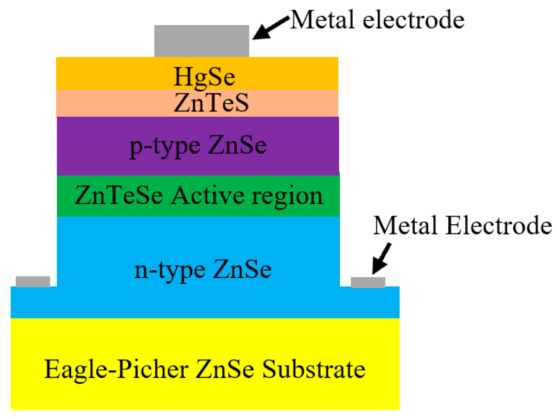
- Eason, D.; Ren, J.; Yu, Z.; Hughes, C.; Cook, J.W., Jr.; Schetzina, J.F.; El-Masry, N.A.; Cantwell, G.; Harsh, W.C. Blue and green light-emitting diode structures grown by molecular beam epitaxy on ZnSe substrates. J. Cryst. Growth 1995, 150, 718–724. [Google Scholar] [CrossRef]
- Su, Y.K.; Wu, M.C.; Chang, C.Y.; Cheng, K.Y. The fabrication of single heterojunction AlGaAs/InGaP electroluminescent diodes. J. Appl. Phys. 1987, 62, 2541–2544. [Google Scholar] [CrossRef]
- Baldo, M.A.; O’Brien, D.; You, Y.; Shoustikov, A.; Sibley, S.P.; Thompson, M.E.; Forrest, S.R. Highly efficient phosphorescent emission from organic electroluminescent devices. Nature 1998, 395, 151–154. [Google Scholar] [CrossRef]
- Pal, B.; Ghosh, Y.; Brovelli, S.; Laocharoensuk, R.; Klimov, V.; Hollingsworth, J.; Htoon, H. ‘Giant’ CdSe/CdS core/shell Nanocrystal Quantum Dots as Efficient Electroluminescent Materials: Strong Influence of Shell Thickness on Light-Emitting Diode Performance. Nano Lett. 2011, 12, 331–336. [Google Scholar] [CrossRef] [PubMed]
- Kim, Y.; Cho, H.; Heo, J.; Kim, T.; Myoung, N.; Lee, C.; Im, L.; Lee, W. Multicolored organic/inorganic hybrid perovskite light-emitting diodes. Adv. Mater. 2014, 27, 1248–1254. [Google Scholar] [CrossRef]
- Jung, B.; Lee, W.; Kim, J.; Choi, M.; Shin, H.; Joo, M.; Jung, S.; Choi, Y.; Kim, M. Enhancement in external quantum efficiency of AlGaNP red μ-led using chemical solution treatment process. Sci. Rep. 2021, 11, 4535. [Google Scholar] [CrossRef]
- Sutherland, B.R. Perovskite photonic sources. Nat. Photonics 2016, 10, 295–302. [Google Scholar] [CrossRef]
- Kwak, J.; Bae, W.; Lee, D.; Park, I.; Lim, J.; Park, M.; Cho, H.; Woo, H.; Yoon, D.; Char, K.; et al. Bright and efficient full-color colloidal quantum dot light-emitting diodes using an inverted device structure. Nano Lett. 2012, 12, 2362–2366. [Google Scholar] [CrossRef] [PubMed]
- Leyden, M.; Meng, L.; Jiang, Y.; Ono, L.; Qiu, L.; Juárez-Pérez, E.; Qin, C.; Adachi, C.; Qi, Y. Methylammonium lead bromide perovskite light-emitting diodes by chemical vapor deposition. J. Phys. Chem. Lett. 2017, 8, 3193–3198. [Google Scholar] [CrossRef] [PubMed]
- Jagadhane, K.; Butcher, R.; Dongale, T.; Nirmal, K.; Kolekar, G.; Tamboli, M.; Kim, T.; Salunke-Gawali, S.; Anbhule, P. Multifunctional fluorescent tetraphenylethene-based reversible mechanochromism for highly selective detection of MnO4− in aqueous media and green organic light emitting diode applications. Cryst. Growth Des. 2023, 23, 4164–4179. [Google Scholar] [CrossRef]
- Uthirakumar, P.; Hong, C.; Suh, E.K.; Lee, Y. Novel fluorescent polymer/zinc oxide hybrid particles: synthesis and application as a luminescence converter for white light-emitting diodes. Chem. Mater. 2006, 18, 4990–4992. [Google Scholar] [CrossRef]
- Zheng, H.; Zheng, Y.; Liu, N.; Ai, N.; Wang, Q.; Wu, S.; Zhou, J.; Hu, D.; Yu, S.; Han, S.; et al. All-solution processed polymer light-emitting diode displays. Nat. Commun. 2013, 4, 1971. [Google Scholar] [CrossRef] [PubMed]
- Jeon, S.; Jang, S.; Son, H.; Lee, J. External quantum efficiency above 20% in deep blue phosphorescent organic light-emitting diodes. Adv. Mater. 2011, 23, 1436–1441. [Google Scholar] [CrossRef] [PubMed]
- Huang, S.; Yu, Y.; Shang, M.; Sun, Y.; Dang, P.; Lin, J. Super broadband near-infrared solid solution phosphors with adjustable peak wavelengths from 1165 to 875 nm for NIR spectroscopy applications. Adv. Opt. Mater. 2023, 11, 2202291. [Google Scholar] [CrossRef]
- Luo, X.; Xiong, W.; Cheng, T.; Liu, S. Temperature estimation of high-power light emitting diode streetlamp by a multi-chip analytical solution. IET Optoelectron. 2009, 3, 225–232. [Google Scholar] [CrossRef]
- Arık, M.; Becker, C.; Weaver, S.; Petroski, J. Thermal management of LEDs: Package to system. SPIE Proc. 2004, 5187, 64–75. [Google Scholar]
- Wang, R.; Wang, J. Analyzing the structural designs and thermal performance of nonmetal lighting devices of led bulbs. Int. J. Heat Mass Transfer. 2016, 99, 750–761. [Google Scholar] [CrossRef]
- Chuluunbaatar, Z.; Kim, N.Y. Thermal analysis and optimization of 6.4 w Si-based multichip led packaged module. J. Korean Inst. Commun. Sci. 2014, 39, 234–238. [Google Scholar] [CrossRef]
- Hong, D.; Lee, S. A study on high power led lamp structures. Korean J. Opt. Photon. 2010, 21, 118–122. [Google Scholar] [CrossRef]
- Kang, S.; Moon, D.; Jang, J.; Kim, J.; Suh, J.; Yoon, E.; Han, H.; Choi, I. Flaw-containing alumina hollow nanostructures have ultrahigh fracture strength to be incorporated into high-efficiency GaN light-emitting diodes. Nano Lett. 2018, 18, 1323–1330. [Google Scholar] [CrossRef] [PubMed]
- Özgür, U.; Alivov, Y.I.; Liu, C.; Teke, A.; Reshchikov, M.A.; Doğan, S.; Avrutin, V.C.S.J.; Cho, S.J.; Morkoç, A. A comprehensive review of ZnO materials and devices. J. Appl. Phys. 2005, 98, 041301. [Google Scholar] [CrossRef]
- Priller, H.; Brückner, J.; Gruber, T.; Klingshirn, C.; Kalt, H.; Waag, A.; Ko, H.; Yao, T. Comparison of linear and nonlinear optical spectra of various ZnO epitaxial layers and of bulk material obtained by different experimental techniques. Phys. Status Solidi (B) 2004, 241, 587–590. [Google Scholar] [CrossRef]
- Bavencove, A.; Salomon, D.; Lafossas, M.; Martin, B.; Dussaigne, A.; Lévy, F.; Andre, B.; Ferret, P.; Durand, C.; Eymery, J.; et al. Light emitting diodes based on GaN core/shell wires grown by MOVPE on n-type Si substrate. Electron. Lett. 2011, 47, 765–767. [Google Scholar] [CrossRef]
- Gong, X.; Kan, H.; Makino, T.; Watanabe, K.; Iida, T.; Suzuki, H.; Aoyama, M.; Yamaguchi, T. Light emitting diodes fabricated from liquid phase epitaxial InAs/InAsxP1-x-ySby/ InAs/InAsx’P1-x’-y’Sby’’ and InAs/InAs1-xSbx multi-layers. Cryst. Res. Technol. 2000, 35, 549–555. [Google Scholar] [CrossRef]
- Noorprajuda, M.; Ohtsuka, M.; Adachi, M.; Fukuyama, H. AlN formation by an Al/GaN substitution reaction. Sci. Rep. 2020, 10, 13058. [Google Scholar] [CrossRef] [PubMed]
- Akasaki, I.; Amano, H.; Murakami, H.; Sassa, M.; Kato, H.; Manabe, K. Growth of GaN and AlGaN for UV/blue p-n junction diodes. J. Cryst. Growth 1993, 128, 379–383. [Google Scholar] [CrossRef]
- Edmond, J.; Abare, A.; Bergman, M.; Bharathan, J.; Bunker, K.; Emerson, D.; Haberern, K.; Ibbetson, J.; Leung, M.; Russel, P.; et al. High efficiency GaN-based LEDs and lasers on SiC. J. Cryst. Growth 2004, 272, 242–250. [Google Scholar] [CrossRef]
- Muramoto, Y.; Kimura, M.; Nouda, S. Development and future of ultraviolet light-emitting diodes: UV-LED will replace the UV lamp. Semicond. Sci. Technol. 2014, 29, 084004. [Google Scholar] [CrossRef]
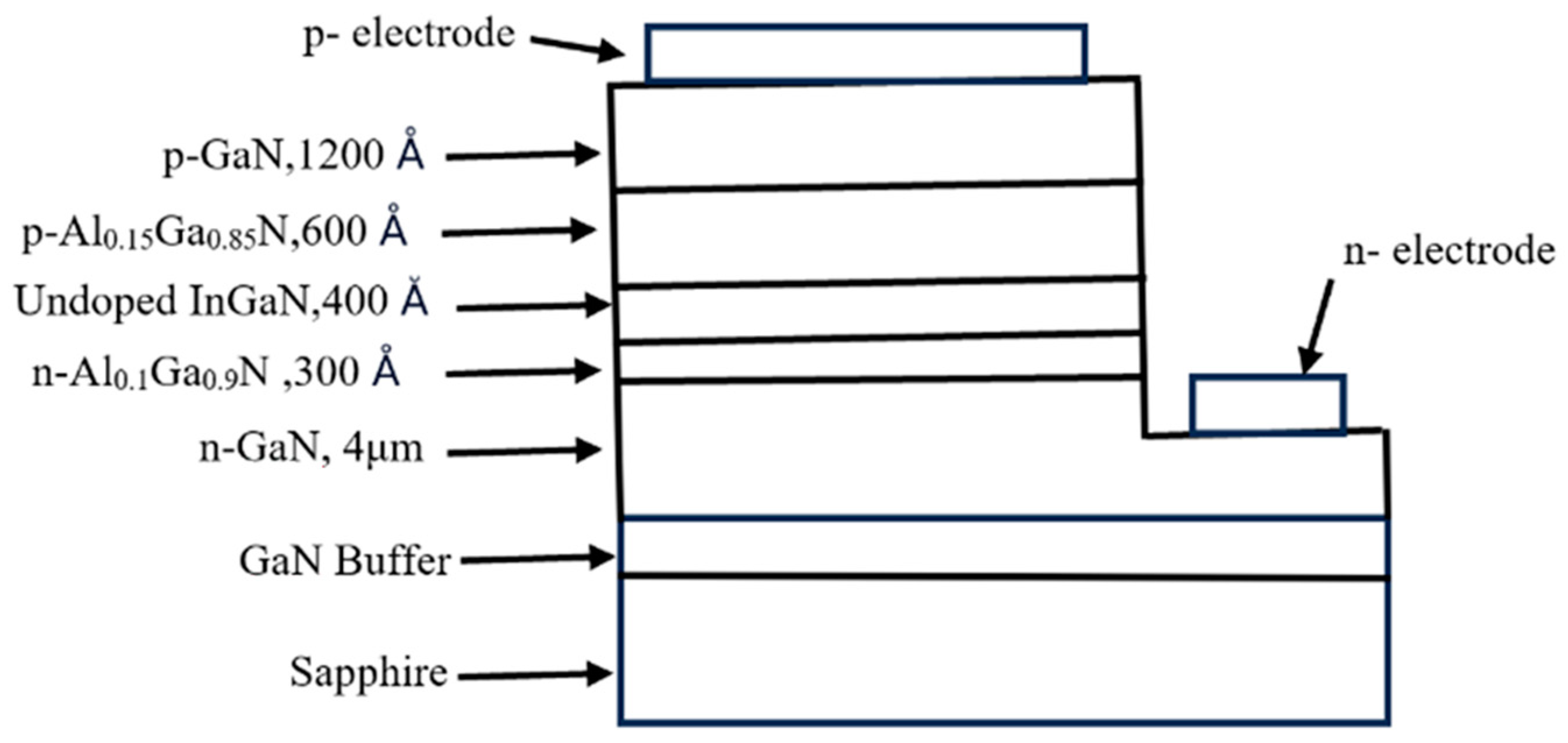
- Oh, J.; Moon, Y.; Kang, D.; Park, C.; Han, J.; Jung, M.; Sung, Y.; Jeong, H.; Song, J.; Seong, T. High efficiency ultraviolet GaN-based vertical light emitting diodes on 6-inch sapphire substrate using ex-situ sputtered AlN nucleation layer. Opt. Express 2018, 26, 5111–5117. [Google Scholar] [CrossRef] [PubMed]
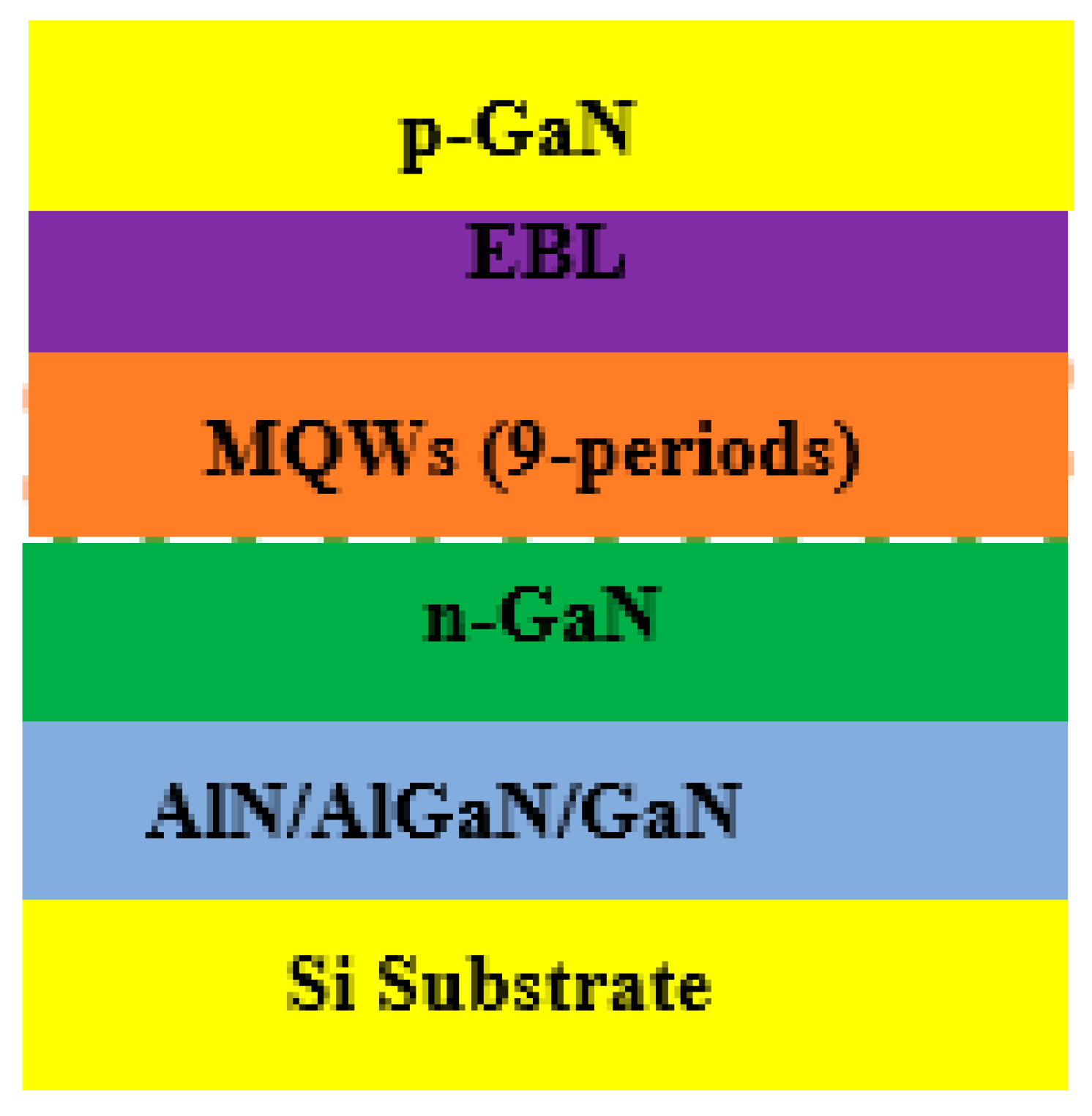
- Li, Y.; Xing, Z.; Zheng, Y.; Tang, X.; Xie, W.; Chen, X.; Wang, W.; Li, G. High-efficiency near-UV light-emitting diodes on Si substrates with InGaN/GaN/AlGaN/GaN multiple quantum wells. J. Mater. Chem. C 2020, 8, 883–888. [Google Scholar] [CrossRef]
- Shur, M.S.; Gaska, R. Deep-Ultraviolet Light-Emitting Diodes. IEEE Trans. Electron. Devices 2010, 57, 12–25. [Google Scholar] [CrossRef]
- Hirayama, H.; Fujikawa, S.; Noguchi, N.; Norimatsu, J.; Takano, T.; Tsubaki, K.; Kamata, N. 222-282 nm AlGaN and InAlGaN-based deep-UV LEDs fabricated on high-quality AlN on sapphire. Phys. Status Solidi A 2009, 206, 1176–1182. [Google Scholar] [CrossRef]
- Fujioka, A.; Misaki, T.; Murayama, T.; Narukawa, Y.; Mukai, T. Improvement in Output Power of 280-nm Deep Ultraviolet Light-Emitting Diode by Using AlGaN Multi Quantum Wells. Appl. Phys. Express 2010, 3, 041001. [Google Scholar] [CrossRef]
- Shatalov, M.; Sun, W.; Lunev, A.; Hu, X.; Dobrinsky, A.; Bilenko, Y.; Yang, J.; Shur, M.; Gaska, R.; Moe, C.; et al. AlGaN Deep-Ultraviolet Light-Emitting Diodes with External Quantum Efficiency above 10%. Appl. Phys. Express 2012, 5, 082101. [Google Scholar] [CrossRef]
- Takano, T.; Mino, T.; Sakai, J.; Noguchi, N.; Tsubaki, K.; Hirayama, H. Deep-ultraviolet light-emitting diodes with external quantum efficiency higher than 20% at 275 nm achieved by improving light-extraction efficiency. Appl. Phys. Express 2017, 10, 031002. [Google Scholar] [CrossRef]
- Maeda, N.; Jo, M.; Hasegawa, H. Improving the Efficiency of AlGaN Deep-UV LEDs by Using Highly Reflective Ni/Al p-Type Electrodes. Phys. Status Solidi A 2018, 215, 1700435. [Google Scholar] [CrossRef]
- Pandey, A.; Shin, W.; Gim, J.; Hovden, R.; Mi, Z. High-efficiency AlGaN/GaN/AlGaN tunnel junction ultraviolet light-emitting diodes. Photon. Res. 2020, 8, 331–337. [Google Scholar] [CrossRef]
- Zheng, Z.; Chen, Q.; Dai, J.; Wang, A.; Liang, R.; Zhang, Y.; Shan, M.; Wu, F.; Zhang, W.; Chen, C.; et al. Enhanced light extraction efficiency via double nano-pattern arrays for high-efficiency deep UV LEDs. Opt. Laser Technol. 2021, 143, 107360. [Google Scholar] [CrossRef]
- Chen, K.; Dai, Q.; Lee, W.; Kim, J.; Schubert, E.; Grandusky, J.; Mendrick, M.; Li, X.; Smart, J. Effect of dislocations on electrical and optical properties of n-type Al0.34Ga0.66N. Appl. Phys. Lett. 2008, 93, 192108. [Google Scholar] [CrossRef]
- Nam, K.B.; Li, J.; Nakarmi, M.L.; Lin, J.Y.; Jiang, H.X. Unique optical properties of AlGaN alloys and related ultraviolet emitters. Appl. Phys. Lett. 2004, 84, 5264–5266. [Google Scholar] [CrossRef]
- Kuo, Y.-K.; Chang, J.-Y.; Chen, F.-M.; Shih, Y.-H.; Chang, H.-W. Numerical Investigation on the Carrier Transport Characteristics of AlGaN Deep-UV Light-Emitting Diodes. IEEE J. Quantum Electron. 2016, 52, 1–5. [Google Scholar] [CrossRef]
- Chitnis, A.; Sun, J.; Mandavilli, V.; Pachipulusu, R.; Wu, S.; Gaevski, M.; Adivarahan, V.; Zhang, J.; Khan, M.; Sarua, A. Kuball, M. Self-heating effects at high pump currents in deep ultraviolet light-emitting diodes at 324 nm. Appl. Phys. Lett. 2002, 81, 3491–3493. [Google Scholar] [CrossRef]
- Mondal, R.K.; Adhikari, S.; Chatterjee, V.; Pal, S. Recent advances and challenges in AlGaN-based ultra-violet light emitting diode technologies. Mater. Res. Bull. 2021, 140, 111258. [Google Scholar] [CrossRef]
- Chadi, D.J. Doping in ZnSe, ZnTe, MgSe, MgTe wide-bandgap semiconductors. Phys. Rev. Lett. 1994, 72, 534. [Google Scholar] [CrossRef]
- Gogova, D.; Kasic, A.; Larsson, H.; Pécz, B.; Yakimova, R.; Magnusson, B.; Monemar, B.; Tuomisto, F.; Saarinen, K.; Miskys, C.; et al. Optical and structural characteristics of virtually unstrained bulk-like GaN. J. Appl. Phys. 2004, 43, 1264. [Google Scholar] [CrossRef]
- Ned, A. Why Blue LED Earned a Nobel Prize if Reds and Greens Already Existed for Decades? In Predict: 10 March 2021. Available online: https://medium.com/predict/why-blue-led-earned-nobel-prize-if-reds-and-greens-already-existed-for-decades-d03e31a6fd8f (accessed on 15 January 2024).
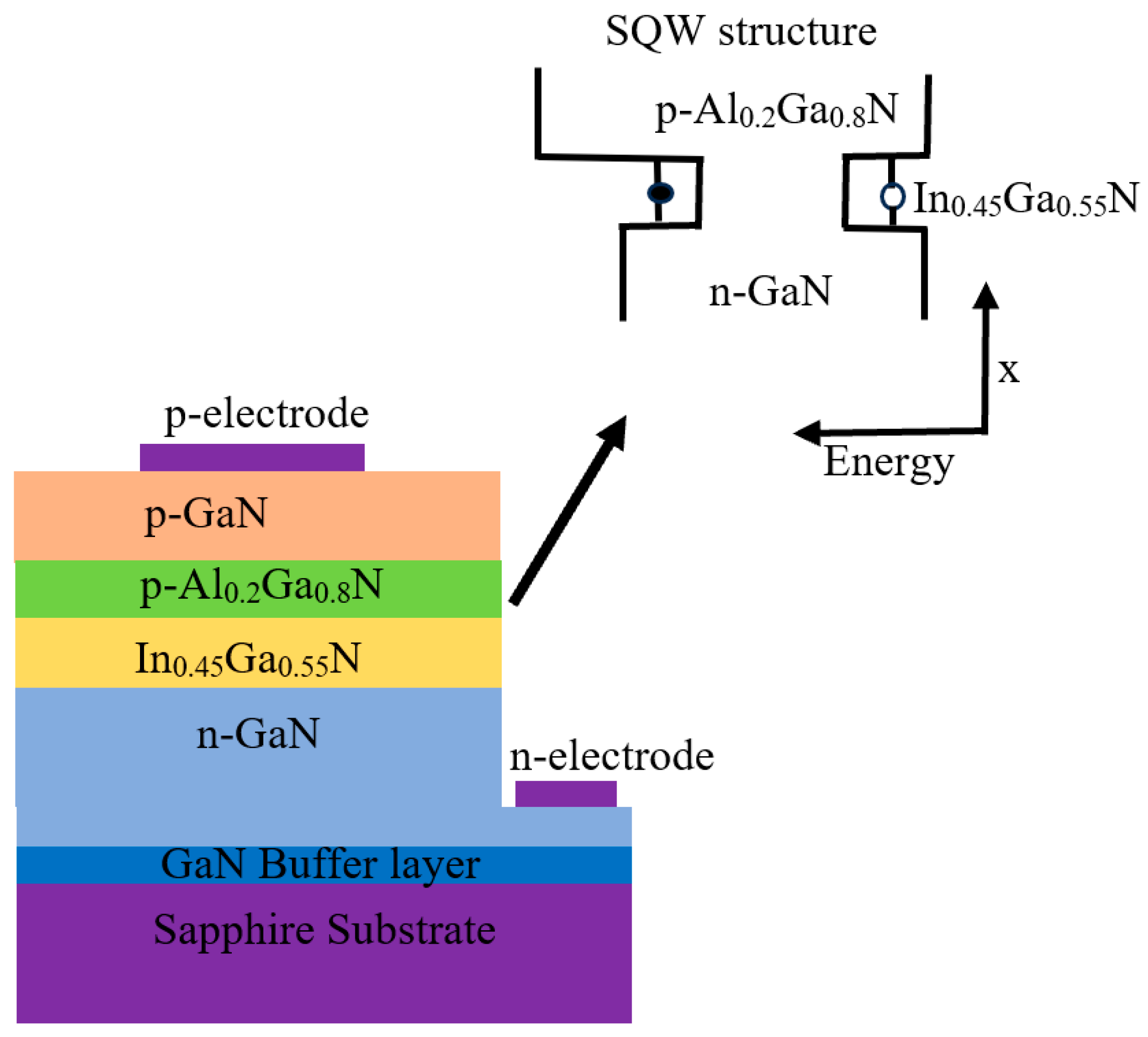
- Nakamura, S.; Senoh, M.; Mukai, T. P-GaN/N-InGaN/N-GaN Double-Heterostructure Blue-Light-Emitting Diodes. Jpn. J. Appl. Phys. 1993, 32, L8–L11. [Google Scholar] [CrossRef]
- Craford, M.G. From Holonyak to Today. Proc. IEEE 2013, 101, 2170–2175. [Google Scholar] [CrossRef]
- Brahmbhatt, G. Blue LEDs Will Have a Significant Positive Impact on Lighting Costs & the Environment. Available online: https://www.bisinfotech.com/blue-leds-will-have-a-significant-positive-impact-on-lighting-costs-the-environment/ (accessed on 20 January 2024).
- Krames, M.; Shchekin, O.; Mueller-Mach, R.; Mueller, G.; Zhou, L.; Harbers, G.; Craford, M. Status and Future of High-Power Light-Emitting Diodes for Solid-State Lighting. J. Disp. Technol. 2007, 3, 160–175. [Google Scholar] [CrossRef]
- Nakamura, S.; Mukai, T.; Senoh, M.; Iwasa, N. Thermal Annealing Effects on P-Type Mg-Doped GaN Films. Jpn. J. Appl. Phys. 1992, 31, L139–L142. [Google Scholar] [CrossRef]
- Nakamura, S.; Iwasa, N.; Masayuki Senoh, M.S.; Takashi Mukai, T.M. Hole Compensation Mechanism of P-Type GaN Films. Jpn. J. Appl. Phys. 1992, 31, 1258. [Google Scholar] [CrossRef]
- Amano, H.; Kito, M.; Hiramatsu, K.; Akasaki, I. P-Type Conduction in Mg-Doped GaN Treated with Low-Energy Electron Beam Irradiation (LEEBI). Jpn. J. Appl. Phys. 1989, 28, L2112–L2114. [Google Scholar] [CrossRef]
- Nakamura, S.; Mukai, T. High-Quality InGaN Films Grown on GaN Films. Jpn. J. Appl. Phys. 1992, 31, L1457–L1459. [Google Scholar] [CrossRef]
- Nakamura, S. GaN Growth Using GaN Buffer Layer. Jpn. J. Appl. Phys. 1991, 30, L1705–L1707. [Google Scholar] [CrossRef]
- Amano, H.; Sawaki, N.; Akasaki, I.; Toyoda, Y. Metalorganic vapor phase epitaxial growth of a high quality GaN film using an AlN buffer layer. Appl. Phys. Lett. 1986, 48, 353–355. [Google Scholar] [CrossRef]
- Kimura, S.; Yoshida, H.; Uesugi, K.; Ito, T.; Okada, A.; Nunoue, S. Performance enhancement of blue light-emitting diodes with InGaN/GaN multi-quantum wells grown on Si substrates by inserting thin AlGaN interlayers. J. Appl. Phys. 2016, 120, 113104. [Google Scholar] [CrossRef]
- Hou, S.; Gangishetty, M.K.; Quan, Q.; Congreve, D.N. Efficient blue and white perovskite light-emitting diodes via manganese doping. Joule 2018, 2, 2421–2433. [Google Scholar] [CrossRef]
- Vashishtha, P.; Ng, M.; Shivarudraiah, S.B.; Halpert, J.E. High efficiency blue and green light-emitting diodes using Ruddlesden–Popper inorganic mixed halide perovskites with butylammonium interlayers. Chem. Mater. 2018, 31, 83–89. [Google Scholar] [CrossRef]
- The History of LED Lighting—Energysavinglighting.org. 19 November 2019. Available online: https://www.energysavinglighting.org/the-history-of-led-lighting/ (accessed on 16 January 2024).
- Bush, S. 50 Year History of the LED. Electronics Weekly. 22 September 2010. Available online: https://www.electronicsweekly.com/news/products/led/50-year-history-of-the-led-2-2010-09/#:~:text=With%20his%20PhD%20from%20Illinois (accessed on 16 January 2024).
- Akasaki, I. Fascinating journeys into blue light (Nobel Lecture). Ann. Phys. 2015, 527, 311–326. [Google Scholar] [CrossRef]
- Eason, D.B.; Yu, Z.; Hughes, W.C.; Roland, W.H.; Boney, C.; Cook, J.W., Jr.; Schetzina, J.F.; Cantwell, G.; Harsch, W.C. High-brightness blue and green light-emitting diodes. Appl. Phys. Lett. 1995, 66, 115–117. [Google Scholar] [CrossRef]
- Nakamura, S. Present performance of InGaN-based blue/green/yellow LEDs. Proc. SPIE 1997, 3002, 26–35. [Google Scholar]
- Peter, M.; Laubsch, A.; Bergbauer, W.; Meyer, T.; Sabathil, M.; Baur, J.; Hahn, B. New developments in green LEDs. Phys. Status Solidi A 2009, 206, 1125–1129. [Google Scholar] [CrossRef]
- 3M Claims Record Efficacy for Green LEDs. Technology. 28 July 2010. Available online: https://www.led-professional.com/technology/light-generation/3m-claims-record-efficacy-for-green-leds (accessed on 17 January 2024).
- Yan, C.; Bai, S.; Nie, T.; Wang, V. High-power high-efficiency green LEDs. In Proceedings of the 2015 12th China International Forum on Solid State Lighting (SSLCHINA), Shenzhen, China, 2–4 November 2015; pp. 1–3. [Google Scholar]
- Alhassan, A.I.; Farrell, R.M.; Saifaddin, B.; Mughal, A.; Wu, F.; DenBaars, S.P.; Nakamura, S.; Speck, J.S. High luminous efficacy green light-emitting diodes with AlGaN cap layer. Opt. Express 2016, 24, 17868–17873. [Google Scholar] [CrossRef]
- Li, P.P.; Zhao, Y.B.; Li, H.J.; Che, J.M.; Zhang, Z.H.; Li, Z.C.; Zhang, Y.Y.; Wang, L.C.; Liang, M.; Yi, X.Y.; et al. Very high external quantum efficiency and wall-plug efficiency 527 nm InGaN green LEDs by MOCVD. Opt. Express 2018, 26, 33108–33115. [Google Scholar] [CrossRef]
- Hu, X.; Xiao, F.; Zhou, Q.; Zheng, Y.; Liu, W. High-luminous efficacy green light-emitting diodes with InGaN/GaN quasi-superlattice interlayer and Al-doped indium tin oxide film. J. Alloys Compd. 2019, 794, 137–143. [Google Scholar] [CrossRef]
- Wright, A.; Nelson, J.M. Consistent structural properties for AlN, GaN, and InN. Phys. Rev. B 1995, 51, 7866–7869. [Google Scholar] [CrossRef]
- Zhuang, Z.; Iida, D.; Ohkawa, K. InGaN-based red light-emitting diodes: From traditional to micro-LEDs. Jpn. J. Appl. Phys. 2021, 61, SA0809. [Google Scholar] [CrossRef]
- Iwasaki, Y.; Motomura, G.; Tsuzuki, T. Pure-colored red, green, and blue quantum dot light-emitting diodes using emitting layers composed of cadmium-free quantum dots and organic electron-transporting materials. Jpn. J. Appl. Phys 2022, 61, 052004. [Google Scholar] [CrossRef]
- Holonyak, N.; Bevacqua, S.F. Coherent (visible) light emission from Ga (As1-xPx) junctions. Appl. Phys. Lett. 1962, 1, 82–83. [Google Scholar] [CrossRef]
- Gershenzon, M.; Logan, R.A.; Nelson, D.F. Electrical and Electroluminescent Properties of Gallium Phosphide Diffused p-n Junctions. Phys. Rev. 1966, 149, 580–597. [Google Scholar] [CrossRef]
- Nair, G.B.; Dhoble, S.J. A perspective perception on the applications of light-emitting diodes. Luminescence 2015, 30, 1167–1175. [Google Scholar] [CrossRef] [PubMed]
- Kish, F.A.; Steranka, F.M.; DeFevere, D.C.; Vanderwater, D.A.; Park, K.G.; Kuo, C.P.; Osentowski, T.D.; Peanasky, M.J.; Yu, J.G.; Fletcher, R.M.; et al. Very high-efficiency semiconductor wafer-bonded transparent-substrate(AlxGa1−x)0.5In0.5P/GaP light-emitting diodes. Appl. Phys. Lett. 1994, 64, 2839–2841. [Google Scholar] [CrossRef]
- Osram Increases LED Efficiency. Photonics Spectra. 28 July 2010. Available online: https://www.photonics.com/Articles/Osram_Increases_LED_Efficiency_/a43266 (accessed on 17 February 2024).
- 609 nm Red LED Prototype from OSRAM Opto Semiconductors Achieves Record Efficiency. LED Professional—LED Lighting. Technology, Application Magazine. 17 October 2011. Available online: https://www.led-professional.com/technology/light-generation/609-nm-red-led-prototype-from-osram-opto-semiconductors-achieves-record-efficiency (accessed on 11 February 2024).
- Pattison, P.M.; Hansen, M.; Tsao, J.Y. LED lighting efficacy: Status and directions. C R. Phys. 2018, 19, 134–145. [Google Scholar] [CrossRef]
- Bergh, A.A.; Dean, P.J. Light-emitting diodes. Proc. IEEE 1972, 60, 156–223. [Google Scholar] [CrossRef]
- Bergh, A.A. Bulk degradation of GaP red LEDs. IEEE Trans. Electron. Devices 1971, 18, 166–170. [Google Scholar] [CrossRef]
- 2022 Solid-State Lighting R&D Opportunities. DOE BTO Solid-State Lighting Program, “2022 DOE SSL R&D Opportunities”. February 2022. Available online: https://www.energy.gov/eere/ssl/articles/2022-solid-state-lighting-rd-opportunities (accessed on 17 February 2024).
- Pasayat, S.S.; Gupta, C.; Wong, M.S.; Ley, R.; Gordon, M.J.; DenBaars, S.P.; Nakamura, S.; Keller, S.; Mishra, U.K. Demonstration of ultra-small (<10 μm) 632 nm red InGaN micro-LEDs with useful on-wafer external quantum efficiency (>0.2%) for mini-displays. Appl. Phys. Express. 2020, 14, 011004. [Google Scholar]
- Dussaigne, A.; Le Maitre, P.; Haas, H.; Pillet, J.C.; Barbier, F.; Grenier, A.; Michit, N.; Jannaud, A.; Templier, R.; Vaufrey, D.; et al. Full InGaN red (625 nm) micro-LED (10 μm) demonstration on a relaxed pseudo-substrate. Appl. Phys. Express 2021, 14, 092011. [Google Scholar] [CrossRef]
- Iida, D.; Kirilenko, P.; Velazquez-Rizo, M.; Zhuang, Z.; Najmi, M.A.; Ohkawa, K. Demonstration of 621-nm-wavelength InGaN-based single-quantum-well LEDs with an external quantum efficiency of 4.3% at 10.1 A/cm2. AIP Adv. 2022, 12, 065125. [Google Scholar] [CrossRef]
- Tan, Z.; Moghaddam, R.; Lai, M.; Docampo, P.; Higler, R.; Deschler, F.; Price, M.; Sadhanala, A.; Pazos, L.M.; Credgington, D.; et al. Bright light-emitting diodes based on organometal halide perovskite. Nat. Nanotech. 2014, 9, 687–692. [Google Scholar] [CrossRef] [PubMed]
- Wang, N.; Mei, T.; Yang, X.; Li, H.; Zhu, N.; Zhang, M. Local doping modulation for improving quantum efficiency in gan-based light-emitting diodes. Jpn. J. Appl. Phys. 2013, 52, 112102. [Google Scholar] [CrossRef]
- Bae, W.; Park, Y.; Lim, J.; Lee, D.; Padilha, L.; McDaniel, H.; Robel, I.; Lee, C.; Pietryga, J.; Klimov, V. Controlling the influence of auger recombination on the performance of quantum-dot light-emitting diodes. Nat. Commun. 2013, 4, 2661. [Google Scholar] [CrossRef] [PubMed]
- Lu, M.; Zhang, X.; Zhang, Y.; Guo, J.; Shen, X.; Yu, W.; Rogach, A. Simultaneous strontium doping and chlorine surface passivation improve luminescence intensity and stability of cspbi3 nanocrystals enabling efficient light-emitting devices. Adv. Mater. 2018, 30, 1804691. [Google Scholar] [CrossRef] [PubMed]
- Bierhuizen, S.; Krames, M.; Harbers, G.; Weijers, G. Performance and trends of high power light emitting diodes. In Proceedings of the Seventh International Conference on Solid State Lighting ICSSL7, San Diego, CA, USA, 27–29 August 2007; SPIE: San Diego, CA, USA, 2007; Volume 6669, pp. 53–64. [Google Scholar]
- Vishnuram, P.; Narayanamoorthi, R.; Vijayakumar, K.; Bajaj, M.; Shouran, M.; Samad, B.A.; Kamel, S. A comprehensive review on various non-isolated power converter topologies for a light-emitting diode driver. Front. Energy Res. 2022, 10, 1055258. [Google Scholar] [CrossRef]
- Phan, D.T.; Mondal, S.; Tran, L.H.; Thien, V.T.M.; Van Nguyen, H.; Nguyen, C.H.; Park, S.; Choi, J. A flexible, and wireless LED therapy patch for skin wound photomedicine with IoT-connected healthcare application. Flex. Print. Electron. 2021, 6, 045002. [Google Scholar] [CrossRef]
- Pearton, S.J.; Kang, B.S.; Kim, S.; Ren, F.; Gila, B.P.; Abernathy, C.R.; Lin, J. GaN-based diodes and transistors for chemical, gas, biological and pressure sensing. J. Phys. Condens. Matter 2004, 16, R961. [Google Scholar] [CrossRef]
- Chen, H.; Yeh, T.H.; He, J.; Zhang, C.; Abbel, R.; Hamblin, M.R.; Huang, Y.; Lanzafame, R.J.; Stadler, I.; Celli, J.; et al. Flexible quantum dot light-emitting devices for targeted photo medical applications. J. Soc. Inf. Disp. 2018, 26, 296–303. [Google Scholar] [CrossRef] [PubMed]
- Jeon, Y.; Noh, I.; Seo, Y.C.; Han, J.H.; Park, Y.; Cho, E.H.; Choi, K.C. Parallel-stacked flexible organic light-emitting diodes for wearable photodynamic therapeutics and color-tunable optoelectronics. ACS Nano 2020, 14, 15688–15699. [Google Scholar] [CrossRef]
- Cho, I.H.; Anoop, G.; Suh, D.W.; Lee, S.J.; Yoo, J.S. On the stability and reliability of Sr1-xBaxSi2O2N2:Eu2+ phosphors for white LED applications. Opt. Mater. Express 2012, 2, 1292–1305. [Google Scholar] [CrossRef]
- Anoop, G.; Kim, K.P.; Suh, D.W.; Cho, I.H.; Yoo, J.S. Optical Characteristics of Sr2Si3O2N4:Eu2+ Phosphors for White Light Emitting Diodes. Electrochem. Solid-State Lett. 2011, 14, J58. [Google Scholar] [CrossRef]
- Taguchi, T. Technical trends and future view of white LED lighting, Headline Review. OHM 2004, 5, 8–9. [Google Scholar]
- Taguchi, T. Present Status of Energy Saving Technologies and Future Prospect in White LED Lighting. IEEJ Trans. Electr. Electron. Eng. 2007, 3, 21–26. [Google Scholar] [CrossRef]
- Bergh, A.; Craford, G.; Duggal, A.; Haitz, R. The Promise and Challenge of Solid-State Lighting. Phys. Today 2001, 54, 42–47. [Google Scholar] [CrossRef]
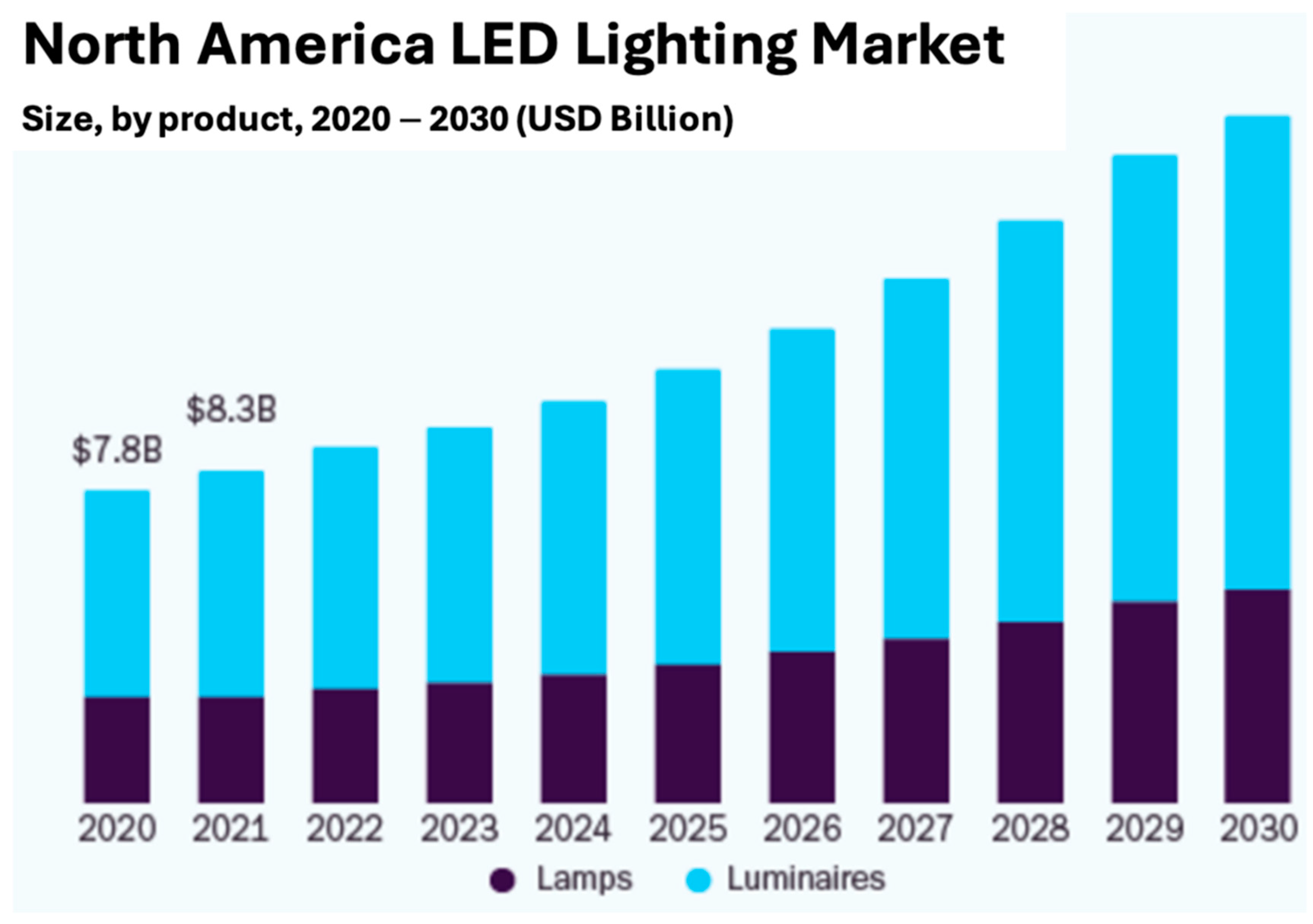
- LED Lighting Market Size, Share & Growth Report, 2020–2030 Industry Report. Available online: https://www.grandviewresearch.com/industry-analysis/led-lighting-market (accessed on 15 September 2023).
- Tang, C.W.; VanSlyke, S.A. Organic electroluminescent diodes. Appl. Phys. Lett. 1987, 51, 913–915. [Google Scholar] [CrossRef]
- Kulkarni, A.P.; Tonzola, C.J.; Babel, A.; Jenekhe, S.A. Electron transport materials for organic light-emitting diodes. Chem. Mater. 2004, 16, 4556–4573. [Google Scholar] [CrossRef]
- Cole, C.M.; Kunz, S.V.; Baumann, T.; Blinco, J.P.; Sonar, P.; Barner-Kowollik, C.; Yambem, S.D. Flexible Inkjet Printed Polymer Light-Emitting Diodes using a Self-Hosted Non-Conjugated TADF Polymer. Macromol. Rapid Commun. 2023, 44, 2300015. [Google Scholar] [CrossRef] [PubMed]
- Huang, C.C.; Xue, M.M.; Wu, F.P.; Yuan, Y.; Liao, L.S.; Fung, M.K. Deep-blue and hybrid-white organic light emitting diodes based on a twisting carbazole-benzofuro [2, 3-b] pyrazine fluorescent emitter. Molecules 2019, 24, 353. [Google Scholar] [CrossRef]
- Xu, Z.; Yu, D.; Yu, M. Synthesis and photophysical properties of novel 4-aryl substituted thiophen derivatives with a vinyl-quinoline unit. J. Chem. Res. 2013, 37, 441–443. [Google Scholar] [CrossRef]
- Mawphlang, O.I.L.; Kharshiing, E.V. Photoreceptor Mediated Plant Growth Responses: Implications for Photoreceptor Engineering toward Improved Performance in Crops. Front. Plant Sci. 2017, 8, 268784. [Google Scholar] [CrossRef]
- Bula, R.J.; Morrow, R.C.; Tibbitts, T.W.; Barta, D.J.; Ignatius, R.W.; Martin, T.S. Light-emitting Diodes as a Radiation Source for Plants. HortScience 1991, 26, 203–205. [Google Scholar] [CrossRef]
- Hoenecke, M.E.; Bula, R.J.; Tibbitts, T.W. Importance of `Blue’ Photon Levels for Lettuce Seedlings Grown under Red-light-emitting Diodes. HortScience 1992, 27, 427–430. [Google Scholar] [CrossRef] [PubMed]
- Deitzer, G.F.; Hayes, R.M.; Jabben, M. Kinetics and Time Dependence of the Effect of Far Red Light on the Photoperiodic Induction of Flowering in Wintex Barley. Plant Physiol. 1979, 64, 1015–1021. [Google Scholar] [CrossRef] [PubMed]
- Morgan, D.C.; Smith, H. A systematic relationship between phytochrome-controlled development and species habitat, for plants grown in simulated natural radiation. Planta 1979, 145, 253–258. [Google Scholar] [CrossRef] [PubMed]
- Blaauw, O.H.; Blaauw-Jansen, G. The phototropic responses of Avena coleoptiles. Acta Bot. Neerl. 1970, 19, 755–763. [Google Scholar] [CrossRef]
- Schwartz, A.; Zeiger, E. Metabolic energy for stomatal opening. Roles of photophosphorylation and oxidative phosphorylation. Planta 1984, 161, 129–136. [Google Scholar] [CrossRef] [PubMed]
- Whelan, H.T. NASA Light-Emitting Diodes for the Prevention of Oral Mucositis in Pediatric Bone Marrow Transplant Patients. J. Clin. Laser Med. Surg. 2002, 20, 319–324. [Google Scholar] [CrossRef] [PubMed]
- Trelles, M.A. Phototherapy in anti-aging and its photobiologic basics: A new approach to skin rejuvenation. J. Cosmet. Dermatol. 2006, 5, 87–91. [Google Scholar] [CrossRef] [PubMed]
- Khoury, J.G.; Goldman, M.P. Use of light-emitting diode photo modulation to reduce erythema and discomfort after intense pulsed light treatment of photodamage. J. Cosmet. Dermatol. 2008, 7, 30–34. [Google Scholar] [CrossRef]
- Ashkenazi, H.; Malik, Z.; Harth, Y.; Nitzan, Y. Eradication of Propionibacterium acnes by its endogenic porphyrins after illumination with high intensity blue light. FEMS Immunol. Med. Microbiol. 2003, 35, 17–24. [Google Scholar] [CrossRef]
- Ra, Y.H.; Rashid, R.T.; Liu, X.; Lee, J.; Mi, Z. Scalable nanowire photonic crystals: Molding the light emission of InGaN. Adv. Funct. Mat. 2017, 27, 1702364. [Google Scholar] [CrossRef]
- Cheng, C.; Ning, L.; Ke, X.; Molokeev, M.S.; Wang, Z.; Zhou, G.; Chuang, Y.C.; Xia, Z. Designing high-performance LED phosphors by controlling the phase stability via a hetero valent substitution strategy. Adv. Opt. Mat. 2020, 8, 1901608. [Google Scholar] [CrossRef]
- Liu, A.; Mukhin, I.S.; Islamova, R.M.; Tian, J. Flexible Perovskite Light-Emitting Diodes: Characteristics and Performance. Adv. Funct. Mat. 2023, 14, 2312209. [Google Scholar] [CrossRef]
- Heilmeier, G.H.; Zanoni, L.A.; Barton, L.A. Dynamic scattering: A new electrooptic effect in certain classes of nematic liquid crystals. Proc. IEEE 1968, 56, 1162–1171. [Google Scholar] [CrossRef]
- Soref, R.A. Transverse field effects in nematic liquid crystals. Appl. Phys. Lett. 1973, 22, 165–166. [Google Scholar] [CrossRef]
- Lee, J.; Chen, C.; Lee, P.; Lin, H.; Leung, M.; Chiu, T.; Lin, C. Blue organic light-emitting diodes: Current status, challenges, and future outlook. J. Mater. Chem. C 2019, 7, 5874–5888. [Google Scholar] [CrossRef]
- Geffroy, B.; Le Roy, P.; Prat, C. Organic light-emitting diode (OLED) technology: Materials, devices and display technologies. Polym. Int. 2006, 55, 572–582. [Google Scholar] [CrossRef]
- Chen, H.; Tan, G.; Wu, S.-T. Ambient contrast ratio of LCDs and OLED displays. Opt. Express 2017, 25, 33643–33656. [Google Scholar] [CrossRef]
- Lv, X.; Loo, K.H.; Lai, Y.M.; Tse, C.K. Energy-Saving Driver Design for Full-Color Large-Area LED Display Panel Systems. IEEE Trans. Ind. Electron. 2014, 61, 4665–4673. [Google Scholar] [CrossRef]
- Goldman, D. The World is Running Out of Plasma TVs. CNNMoney. 30 October 2014. Available online: https://money.cnn.com/2014/10/30/technology/plasma-tv/index.html (accessed on 18 February 2024).
- Tsujimura, T. OLED Display Fundamentals and Applications, 2nd ed.; John Wiley & Sons: Hoboken, NJ, USA, 2017. [Google Scholar]
- Shafer, R. Mini-LED vs. Micro-LED—What Is the Difference? Display Ninja. 4 December 2023. Available online: https://www.displayninja.com/mini-led-vs-microled/ (accessed on 18 February 2024).
- Seetzen, H.; Heidrich, W.; Stuerzlinger, W.; Ward, G.; Whitehead, L.; Trentacoste, M.; Ghosh, A.; Vorozcovs, A. High Dynamic Range Display Systems. In Seminal Graphics Papers: Pushing the Boundaries; Association for Computing Machinery: New York, NY, USA, 2023; Volume 2, pp. 39–47. [Google Scholar]
- Daly, S.; Kunkel, T.; Sun, X.; Farrell, S.; Crum, P. 41.1: Distinguished Paper: Viewer Preferences for Shadow, Diffuse, Specular, and Emissive Luminance Limits of High Dynamic Range Displays. SID Symp. Dig. Tech. Pap. 2013, 44, 563–566. [Google Scholar] [CrossRef]
- Jiang, H.X.; Jin, S.X.; Li, J.; Shakya, J.; Lin, J.Y. III-nitride blue micro displays. Appl. Phys. Lett. 2001, 78, 1303–1305. [Google Scholar] [CrossRef]
- Tian, P.; McKendry, J.; Gu, E.; Chen, Z.; Sun, Y.; Zhang, G.; Dawson, M.; Liu, R. Fabrication, characterization and applications of flexible vertical InGaN micro-light emitting diode arrays. Opt. Express 2016, 24, 699–707. [Google Scholar] [CrossRef] [PubMed]
- Global Micro-LED Market, Research and Markets. Available online: https://www.researchandmarkets.com/reports/5067415/global-micro-led-market-with-covid-19-impact (accessed on 15 December 2023).
- Matthews, A. Micro-LED Displays Could Disrupt LCD and OLED Supply Chains. Electronic Specifier. 17 February 2017. Available online: https://www.electronicspecifier.com/products/displays/microled-displays-could-disrupt-lcd-and-oled-supply-chains (accessed on 17 December 2023).
- Cok, R.; Meitl, M.; Rotzoll, R.; Melnik, G.; Fecioru, A.; Trindade, A.; Raymond, B.; Bonafede, S.; Gomez, D.; Moore, T.; et al. Inorganic light-emitting diode displays using micro-transfer printing. J. Soc. Inf. Disp. 2017, 25, 589–609. [Google Scholar] [CrossRef]
- Corbett, B.; Loi, R.; Zhou, W.; Liu, D.; Ma, Z. Transfer print techniques for heterogeneous integration of photonic components. Prog. Quantum Electron. 2017, 52, 1–17. [Google Scholar] [CrossRef]
- Zhuang, Z.; Guo, X.; Liu, B.; Hu, F.; Li, Y.; Tao, T.; Dai, J.; Zhi, T.; Xie, Z.; Chen, P.; et al. High Color Rendering Index Hybrid III-Nitride/Nanocrystals White Light-Emitting Diodes. Adv. Funct. Mater. 2015, 26, 36–43. [Google Scholar] [CrossRef]
- Wu, T.; Sher, C.-W.; Lin, Y.; Lee, C.-F.; Liang, S.; Lu, Y.; Chen, S.-W.H.; Guo, W.; Kuo, H.-C.; Chen, Z. Mini-led and micro-led: Promising candidates for the next generation display technology. Appl. Sci. 2018, 8, 1557. [Google Scholar] [CrossRef]
- Gu, Y.; Zhang, L.; Yang, J.K.W.; Yeo, S.P.; Qiu, C.-W. Color generation via subwavelength plasmonic nanostructures. Nanoscale 2015, 7, 6409–6419. [Google Scholar] [CrossRef] [PubMed]
- Huang, Y.M.; Singh, K.; Liu, A.; Lin, C.; Chen, Z.; Wang, K.; Lin, Y.; Liu, Z.; Wu, T.; Kuo, H. Advances in Quantum-Dot-Based Displays. Nanomaterials 2020, 10, 1327. [Google Scholar] [CrossRef]
- Yang, Z.; Gao, M.; Wu, W.; Yang, X.; Sun, X.; Zhang, J.; Wang, H.; Liu, R.; Han, C.; Yang, H.; et al. Recent advances in quantum dot-based light-emitting devices: Challenges and possible solutions. Mater. Today 2019, 24, 69–93. [Google Scholar] [CrossRef]
- Huang, Y.; Hsiang, E.L.; Deng, M.Y.; Wu, S.T. Mini-LED, Micro-LED and OLED displays: Present status and future perspectives. Light Sci. Appl. 2020, 9, 105. [Google Scholar] [CrossRef]
- Liu, X.; Tong, C.; Luo, X.; Li, W.; Liu, Z. P-6.8: Study of mass transfer for micro-LED manufacturing. SID Symposium Dig. Tech. Pap. 2019, 50, 775–778. [Google Scholar] [CrossRef]
- Zhao, H.; Yan, Q.; Wang, J.; Hua, D.X. A Compound Parabolic Concentrator Coupled to an Optical Microlenslet Array for Projection Display. In MME 2016; Atlantis Press: Amsterdam, The Netherlands, 2016; pp. 566–572. [Google Scholar]
- Water | WHO | Regional Office for Africa. 16 May 2024. Available online: https://www.afro.who.int/health-topics/water (accessed on 18 May 2024).
- Ultraviolet Disinfection Guidance Manual for the Final Long Term 2 Enhanced Surface Water Treatment Rule; U.S Environmental Protection Agency: Washington, DC, USA, 2006. Available online: https://www.epa.gov/system/files/documents/2022-10/ultraviolet-disinfection-guidance-manual-2006.pdf (accessed on 19 December 2023).
- Sergejevs, A.; Clarke, C.T.; Allsopp, D.W.E.; Marugan, J.; Jaroenworaluck, A.; Singhapong, W.; Manpetch, P.; Timmers, R.; Casado, C.; Bowen, C.R. A calibrated UV-LED based light source for water purification and characterization of photocatalysis. Photochem. Photobiol. Sci. 2017, 16, 1690–1699. [Google Scholar] [CrossRef] [PubMed]
- Chevremont, A.C.; Boudenne, J.-L.; Coulomb, B.; Farnet, A.-M. Impact of watering with UV-LED-treated wastewater on microbial and physico-chemical parameters of soil. Water Res. 2013, 47, 1971–1982. [Google Scholar] [CrossRef]
- Chevremont, A.C.; Farnet, A.M.; Coulomb, B.; Boudenne, J.L. Effect of coupled UV-A and UV-C LEDs on both microbiological and chemical pollution of urban wastewaters. Sci. Total Environ. 2012, 426, 304–310. [Google Scholar] [CrossRef] [PubMed]
- Buonanno, M.; Randers-Pehrson, G.; Bigelow, A.W.; Trivedi, S.; Lowy, F.D.; Spotnitz, H.M.; Hammer, S.M.; Brenner, D.J. 207-nm UV Light—A Promising Tool for Safe Low-Cost Reduction of Surgical Site Infections. I: In Vitro Studies. PLoS ONE 2013, 8, e76968. [Google Scholar] [CrossRef]
- Buonanno, M.; Ponnaiya, B.; Welch, D.; Stanislauskas, M.; Pehrson, G.R.; Smilenov, L.; Lowy, F.D.; Owens, D.M.; Brenner, D.J. Germicidal efficacy and mammalian skin safety of 222-nm UV light. Radiat. Res. 2017, 187, 493–501. [Google Scholar] [CrossRef] [PubMed]
- Oguma, K.; Kita, R.; Sakai, H.; Murakami, M.; Takizawa, S. Application of UV light emitting diodes to batch and flow-through water disinfection systems. Desalination 2013, 328, 24–30. [Google Scholar] [CrossRef]
- de Carvalho, N.A.; Stachler, E.N.; Cimabue, N.; Bibby, K. Evaluation of Phi6 persistence and suitability as an enveloped virus surrogate. Environ. Sci. Technol. 2017, 51, 8692–8700. [Google Scholar] [CrossRef] [PubMed]
- Turgeon, N.; Toulouse, M.-J.; Martel, B.; Moineau, S.; Duchaine, C. Comparison of five bacteriophages as models for viral aerosol studies. Appl. Environ. Microbiol. 2014, 80, 4242–4250. [Google Scholar] [CrossRef]
- Bhattarai, T.; Ebong, A.; Raja, M.Y.A.; Munir, M. Advancements in 275 nm UV-LED Technology for Deactivation of Bacteriophages, Phi6 and MS2. In Proceedings of the 2023 IEEE HONET, 20th International Conference on Smart Communities, Boca Raton, FL, USA, 4–6 December 2023; pp. 120–125. [Google Scholar]
- Aoyagi, Y.; Takeuchi, M.; Yoshida, K.; Kurouchi, M.; Yasui, N.; Kamiko, N.; Araki, T.; Nanishi, Y. Inactivation of Bacterial Viruses in Water Using Deep Ultraviolet Semiconductor Light-Emitting Diode. J. Environ. Eng. 2011, 137, 1215–1218. [Google Scholar] [CrossRef]
- Bowker, C.; Sain, A.; Shatalov, M.; Ducoste, J. Microbial UV fluence-response assessment using a novel UV-LED collimated beam system. Water Res. 2011, 45, 2011–2019. [Google Scholar] [CrossRef]
- Tseng, C.C.; Li, C.-S. Inactivation of viruses on surfaces by ultraviolet germicidal irradiation. J. Occup. Environ. Hyg. 2007, 4, 400–405. [Google Scholar] [CrossRef]
- Beck, S.E.; Ryu, H.; Boczek, L.A.; Cashdollar, J.L.; Jeanis, K.M.; Rosenblum, J.S.; Lawal, O.R.; Linden, K.G. Evaluating uv-c led disinfection performance and investigating potential dual-wavelength synergy. Water Res. 2017, 109, 207–216. [Google Scholar] [CrossRef] [PubMed]
- Mamane, H.; Shemer, H.; Linden, K.G. Inactivation of E. coli, B. subtilis spores, and MS2, T4, and T7 phage using UV/H2O2 advanced oxidation. J. Hazard. Mater. 2007, 146, 479–486. [Google Scholar] [CrossRef] [PubMed]
- Bar-On, Y.M.; Flamholz, A.; Phillips, R.; Milo, R. Science forum: Sars-cov-2 (COVID-19) by the numbers. eLife 2020, 9, e57309. [Google Scholar] [CrossRef] [PubMed]
- Silverman, A.I.; Boehm, A.B. Systematic review and meta-analysis of the persistence and disinfection of human coronaviruses and their viral surrogates in water and wastewater. Environ. Sci. Technol. Lett. 2020, 7, 544–553. [Google Scholar] [CrossRef] [PubMed]
- Bhattarai, T.; Raja, M.Y.A.; Ebong, A.; Bhutta, M.K. On the nano-engineered III-nitride quantum-wells-based deep-UV light emitting diodes for COVID disinfection applications. In Proceedings of the Second iiScience International Conference 2021: Recent Advances in Photonics and Physical Sciences, Faisalabad, Pakistan, 29–30 March 2021; SPIE: Bellingham, WA, USA, 2021; Volume 11877, pp. 61–66. [Google Scholar]
- Buonanno, M.; Stanislauskas, M.; Ponnaiya, B.; Bigelow, A.W.; Randers-Pehrson, G.; Xu, Y.; Shuryak, I.; Smilenov, L.; Owens, D.M.; Brenner, D.J. 207-nm UV light—A promising tool for safe low-cost reduction of surgical site infections. ii: In-vivo safety studies. PLoS ONE 2016, 11, e0138418. [Google Scholar] [CrossRef] [PubMed]
- Cooke, M. GaN:AlN Superlattice UVC LEDs Boost Light Extraction. Semiconductor-Today. 24 August 2023. Available online: https://www.semiconductor-today.com/news_items/2023/aug/silanna-240823.shtml (accessed on 17 December 2023).
- Nicholls, J.; Anderson, L.; Lee, W.; Ahn, J.J.S.; Baskaran, A.; Bang, H.; Belloeil, M.; Cai, Y.; Campbell, J.; Chai, J.; et al. High performance and high yield sub-240 nm AlN: GaN short period superlattice LEDs grown by MBE on 6 in. sapphire substrates. Appl. Phys. Lett. 2023, 123, 051105. [Google Scholar] [CrossRef]
- Kumar, G.D.; Mishra, A.; Dunn, L.; Townsend, A.; Oguadinma, I.C.; Bright, K.R.; Gerba, C.P. Biocides and novel antimicrobial agents for the mitigation of coronaviruses. Front. Microbiol. 2020, 11, 1351. [Google Scholar]
- Hijnen, W.; Beerendonk, E.; Medema, G.J. Inactivation credit of UV radiation for viruses, bacteria and protozoan (oo) cysts in water: A review. Water Res. 2006, 40, 3–22. [Google Scholar] [CrossRef]
- Buonanno, M.; Welch, D.; Shuryak, I.; Brenner, D.J. Far-UVC light (222 nm) efficiently and safely inactivates airborne human coronaviruses. Sci. Rep. 2020, 10, 1–8. [Google Scholar]
- Bedell, K.; Buchaklian, A.H.; Perlman, S. Efficacy of an automated multiple emitter whole-room ultraviolet-c disinfection system against coronaviruses MHV and MERS-CoV. Infect. Control Hosp. Epidemiol. 2016, 37, 598–599. [Google Scholar] [CrossRef] [PubMed]
- Bucknall, R.A.; King, L.M.; Kapikian, A.Z.; Chanock, R.M. Studies with human coronaviruses ii. some properties of strains 229e and oc43. Proc. Soc. Exp. Biol. Med. 1972, 139, 722–727. [Google Scholar] [CrossRef] [PubMed]
- Kariwa, H.; Fujii, N.; Takashima, I. Inactivation of SARS coronavirus by means of povidone-iodine, physical conditions, and chemical reagents. Jpn. J. Vet. Res. 2004, 52, 105–112. [Google Scholar] [CrossRef] [PubMed]
- Gerchman, Y.; Mamane, H.; Friedman, N.; Mandelboim, M. UV-led disinfection of coronavirus: Wavelength effect. J. Photochem. Photobiol. B Biol. 2020, 212, 112044. [Google Scholar] [CrossRef]
- Ansaldi, F.; Banfi, F.; Morelli, P.; Valle, L.; Durando, P.; Sticchi, L.; Contos, S.; Gasparini, R.; Crovari, P. Sars-CoV, influenza A and syncytial respiratory virus resistance against common disinfectants and ultraviolet irradiation. J. Prev. Med. Hyg. 2004, 45, 5–8. [Google Scholar]


| Wavelength (nm) | Microbes | Disinfection Medium | UV Dose (mJ/cm2) | Log Inactivation | Dose Response mJ/cm2 per log Inactivation | References |
|---|---|---|---|---|---|---|
| 255 | MS2 | Water | 41 | 3.2 | 12.8 | [193] |
| 255 | Ms2 | Water | 60 | 2.3 | 26.1 | [194] |
| 255 | E.Coli | Water | 9 | 2.7 | 3.3 | [194] |
| 254 | Ms2 | Gelatin-based medium | 2.51–6.5 | 2 | 1.25–3.25 | [195] |
| 254 | Phi6 | Gelatin-based medium | 7.75–10 | 2 | 3.87–5 | [195] |
| 260 | MS2 | Double agar layer | 30.3 | 2 | 15.15 | [196] |
| 280 | MS2 | Double agar layer | 38.5 | 2 | 19.5 | [196] |
| 260/280 | MS2 | Double agar layer | 32.8 | 2 | 16.4 | [196] |
Disclaimer/Publisher’s Note: The statements, opinions and data contained in all publications are solely those of the individual author(s) and contributor(s) and not of MDPI and/or the editor(s). MDPI and/or the editor(s) disclaim responsibility for any injury to people or property resulting from any ideas, methods, instructions or products referred to in the content. |
© 2024 by the authors. Licensee MDPI, Basel, Switzerland. This article is an open access article distributed under the terms and conditions of the Creative Commons Attribution (CC BY) license (https://creativecommons.org/licenses/by/4.0/).
Share and Cite
Bhattarai, T.; Ebong, A.; Raja, M.Y.A. A Review of Light-Emitting Diodes and Ultraviolet Light-Emitting Diodes and Their Applications. Photonics 2024, 11, 491. https://doi.org/10.3390/photonics11060491
Bhattarai T, Ebong A, Raja MYA. A Review of Light-Emitting Diodes and Ultraviolet Light-Emitting Diodes and Their Applications. Photonics. 2024; 11(6):491. https://doi.org/10.3390/photonics11060491
Chicago/Turabian StyleBhattarai, Trailokya, Abasifreke Ebong, and Mohammad Yasin Akhtar Raja. 2024. "A Review of Light-Emitting Diodes and Ultraviolet Light-Emitting Diodes and Their Applications" Photonics 11, no. 6: 491. https://doi.org/10.3390/photonics11060491
APA StyleBhattarai, T., Ebong, A., & Raja, M. Y. A. (2024). A Review of Light-Emitting Diodes and Ultraviolet Light-Emitting Diodes and Their Applications. Photonics, 11(6), 491. https://doi.org/10.3390/photonics11060491