1. Introduction
Photonic integrated circuits (PICs) have revolutionized optical communication by enabling the on-chip integration of optical components such as lasers, detectors, waveguides, and modulators [
1,
2,
3]. This technology has now extended its applications to sensing, bioanalytics, and healthcare diagnostics. In 2023, the point-of-care testing segment led the biosensor market with a 47% (USD 13.7B) revenue share, driven by technologies such as highly sensitive sensors for monitoring biomarkers or pathogens in body fluids like sweat, urine, or saliva [
4,
5,
6]. These trends underline the growing demand for user-friendly, low-cost, and fast disposable tests [
7,
8].
To significantly reduce costs and enhance the practicality of photonic devices in point-of-care applications, it is essential to segregate the actives, such as the device itself, from the passives, which include the disposables. The separation not only streamlines the manufacturing process but also introduces challenges related to achieving the precise coupling between single-mode fibers or waveguides across various components, which typically requires stringent fiber–chip alignment tolerances [
9]. Although such accuracy is manageable with photonic assembly equipment typically used in optoelectronic modules for telecom and datacom, it presents a significant challenge in rapid diagnostics solutions where passive fiber-to-chip coupling becomes a constraint when disposable biosensors are intended to be used by untrained users. To overcome this hurdle, a highly tolerant coupling method is necessary to ensure operational simplicity and measurement robustness. The fully passive coupling method aims for repeatability across various independent PIC assemblies after system calibration, eliminating the need for active coupling optimization. Contrary to telecom, a low coupling loss is not imperative for most sensing applications. Our study employs photonic integrated sensor chips based on microring resonators as a possible application example. However, the scope of the investigation here is centered on the coupling system itself, which is designed to be adaptable to a wider range of applications. A comprehensive description of the sensor element is available in [
10]. Additionally, the sensors are contextualized within the framework of other related studies therein.
This work presents a combined photonic and mechanical design, utilizing Si
3N
4-based grating couplers in combination with a three-groove kinematic coupling strategy. Grating couplers are widely used in integrated optics for vertical coupling between optical fibers and PICs [
11]. The research concentrates on achieving coupling in the waveguide plane with larger spot sizes compared to the mode field diameter (MFD) of a single-mode fiber of about 10 µm at the 1550 nm wavelength [
9]. Mechanical kinematic couplings are statically determined structures known for their high repeatability and simple design, which is ideal for the intended application. Our mechanical design for the pluggable system draws inspiration from the foundational work of [
12], which we have tailored to meet the specific requirements of the application.
Previous studies have also addressed the challenge of tolerant, pluggable single-mode fiber-to-PIC couplings. [
13] has developed a concept operating at the 1550 nm wavelength, while [
14] explores the options at 1300 nm. Both studies utilized the silicon-on-insulator (SOI) material platform. In contrast, our PIC employs silicon nitride (Si
3N
4) technology. In the research, the spatial 3 dB alignment tolerance is a critical parameter for the passive coupling systems, alongside the insertion loss and, in certain cases, spectral bandwidth. Details and a comparison to the preliminary results are presented in the discussion in
Section 4. The novelty of our work lies in successfully demonstrating a system that obviates the need for additional micro-lenses or gradient index lens systems, yet still offers comparable tolerance characteristics for passive coupling. Moreover, we have achieved repeatable coupling across 99 independent disposables of identical design, marking an advancement towards practical real-world deployment. To our knowledge, prior demonstrations of consequent repeatable passive coupling, as reported by [
14], have been restricted to employing just a single, individual disposable chip, rather than a series of multiple samples.
2. Photonic Biosensors with Highly Tolerant Grating Couplers
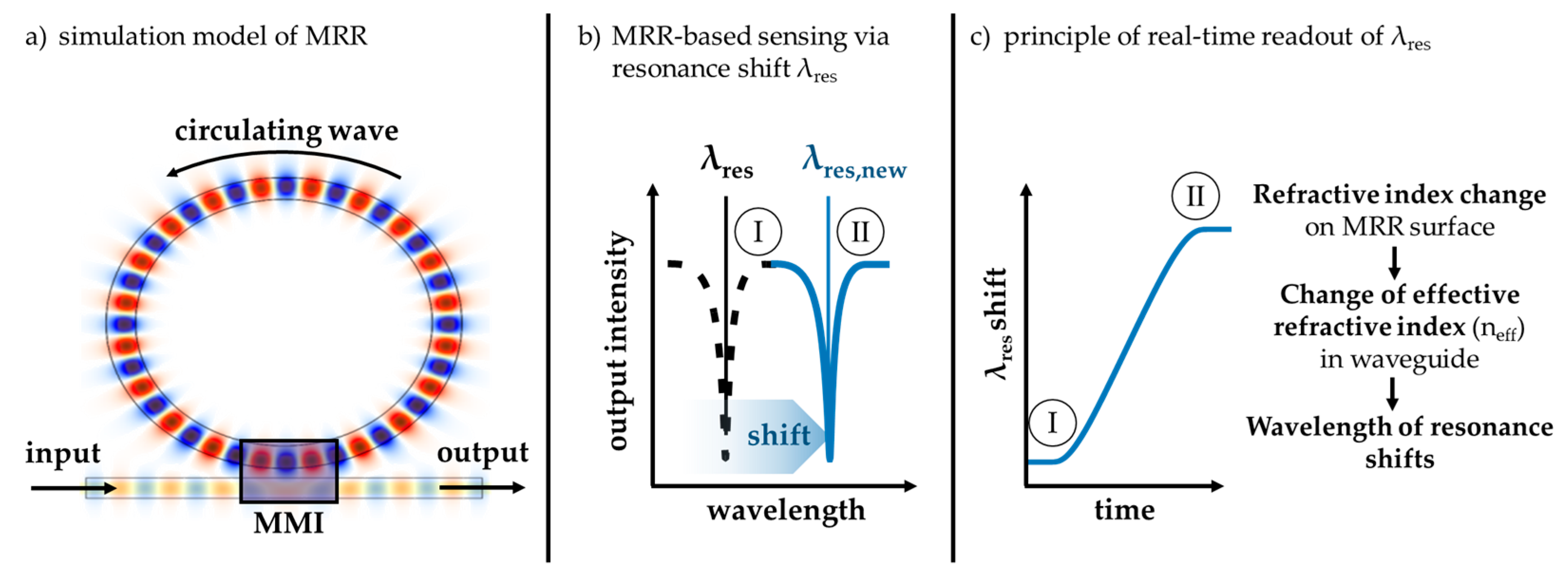
To demonstrate the coupling concept for photonic disposable biosensors, Si
3N
4 PICs with racetrack microring resonators as active sensing elements are used [
15]. The chips feature two sensing channels and are designed to operate in the optical C-band. If light is introduced into the low-confinement single-mode waveguides of the sensor PIC, as illustrated in
Figure 1, an evanescent field is generated along the waveguide core. This field enables the quantitative measurement of, for example, aqueous solution concentrations, by detecting shifts in the MRR resonance wavelength λ
res caused by changes in the refractive indices on the sensor surface [
16]. Additionally, this relative measurement method allows for the qualitative detection of targeted binding events if the sensor is appropriately functionalized [
17].
Further details regarding the used sensor concept can be found in [
10]. The following sections will focus on the key coupling components, as well as their efficiency and usability testing.
The coupling between optical fibers and integrated waveguides is lossy due to the varying dimensions of their mode fields. The assembly through edge-coupling requires a significant amount of effort, which may involve the use of spot size converters to ensure mode size compatibility, as even a slight displacement of a few micrometers results in minimal power transmission [
9]. One solution to mitigate coupling losses and enhance tolerance is the implementation of vertical coupling grating structures in combination with waveguide tapers [
9]. Grating couplers are described by the Bragg condition, as expressed in Equation (1), where N is an integer representing the diffraction order, λ
0 is the free-space wavelength, n
eff is the effective refractive index of the grating, Λ is the grating period, and θ denotes the angle of light diffraction [
18]. The light emitted by the grating exhibits an exponentially decaying power profile along the propagation direction [
19].
When simulating the optimal design parameters for the examined second- and fourth-order grating couplers, the focus was set on ensuring compatibility with straightforward single-etch manufacturing processes and achieving sufficient coupling tolerances for the intended application. Conversely, the coupling efficiency and waveguide propagation loss was considered to be of secondary concern, as a relatively high loss can be accepted when using the relative measurement method due to the sensing MRR principle and the short waveguide distances on the PIC itself.
The performance of the simulated grating structures can be deduced from
Table 1. The optimized gratings achieve a coupling efficiency η of 42% for the second-order coupler and 62% for the fourth-order coupler. To determine the coupling tolerance, the resulting efficiency is analytically calculated by shifting the Gaussian mode from the optimal position identified by the overlap integral. With a spot radius of 60 µm, the second- and fourth-order gratings both exhibit 3 dB tolerances of (lateral/longitudinal) = (50/51) µm. The angular misalignment tolerance is also calculated via an analytical evaluation. An angular misalignment of 1° in the coupling angle results in an approximate additional insertion loss of 9 dB for the second-order grating and about 4 dB for the fourth-order grating. It should be noted that the taper and waveguide losses are comparably small and, hence, were neglected in the simulation. The fidelity of the simulation results was confirmed by a technological and metrological assessment of the test structures, which align with the predictions and especially with the—for this concept, crucial—planar coupling tolerance (see
Section 4.1). Therefore, it was decided to use fourth-order grating couplers for the system design.
Based on the coupling concept, a PIC layout with two MRRs was designed. On the chip, both input and output grating couplers are positioned on the same side for easier coupling. The photonic structures, optimized for the optical C-band, are fabricated on a Si
3N
4 layer as the core material (refractive index n = 1.996). Surrounding this, silicon dioxide (SiO
2, n = 1.444) serves as the cladding material. The fabrication process was carried out on a 4-inch wafer using established PIC technology and includes a layer stack (top to bottom) of 420 nm plasma-enhanced chemical vapor deposition (PECVD) SiO
2, 200 nm low-pressure chemical vapor deposition (LPCVD) Si
3N
4, 3.4 µm thermal SiO
2, and a 525 µm silicon (Si) substrate. The process employs stepper lithography with dry etching and chemical vapor deposition (CVD), as described in [
10,
20]. The MRR waveguides are stripped of the cladding through a lift-off process to create an active sensor area. The high resolution of the stepper lithography is crucial, outperforming contact lithography in defining fine features like the grating patterns.
The waveguides are specifically designed for low confinement, only guiding the transverse electrically (TE) polarized fundamental mode in order to ensure the appropriate interaction of the MRR evanescent field with the medium under analysis. These waveguides are structured with a cross-section of 200 nm by 1500 nm in a ridge waveguide configuration.
The design parameters include a microring cavity radius of 300 µm, and 1 × 2 and 2 × 2 multi-mode interference (MMI) couplers measuring 32.0 µm by 7.5 µm and 87.0 µm by 6.0 µm, respectively, each with a 50% coupling ratio for optical power distribution. The grating couplers are designed with a period of 1.3 µm and a duty cycle of 0.5.
Figure 2 shows a photography of the fabricated sensor chip, measuring 10.0 mm by 8.0 mm, alongside a cross-section image of the waveguide layer.
Prior to assembly, the PICs are initially characterized using a stationary measurement setup (T200S tunable laser with CT440 optical component tester from EXFO Inc., Québec, QC, Canada). For characterization, the transmission spectrum of the sensor chip is acquired in the optical C-band. Key parameters such as the propagation loss of the whole PIC, modulation depth, coupling tolerance, and spectral bandwidth are evaluated due to their critical relevance to the application. The results are summarized in
Section 4.
3. Optomechanical Coupling System for Disposable Photonic Sensors
The performance of the developed grating couplers exhibits relatively high coupling tolerances, thus enabling a fully passive mechanical positioning of a PIC assembly to the photonic system periphery. In the interests of low-cost and user-friendly sensors systems, the disposables must be designed to align automatically when inserted into a read-out unit, allowing light to couple into the waveguide plane without the need for active adjustments of the mounting socket. A preliminary proof-of-concept demonstrating plug-and-play optical alignment is shown in [
14]. Here, a passive single-mode fiber-to-PIC grating coupling was achieved repeatedly (30 times with the same PIC) by using micro-lenses on the chip as well as on the fiber array unit side, facilitated by a positioning construction made of Lego
TM bricks.
In contrast to the method described in [
14], the work presented here requires that various PIC assemblies of the same design have to be passively positioned in the same system for single-use testing without a socket adjustment after a system calibration. The selected approach employs a kinematic coupling strategy, which is described in [
21,
22]. Three-groove kinematic couplings are statically determined structures that are used in precision mountings due to their exceptional passive coupling repeatability, with a literature-mentioned accuracy of less than 0.1 µm [
22]. Instead of small cylinders that interlock as in Lego
TM bricks, matching convex (ball) and concave (groove) elements are used. Additionally, the simplicity and, therefore, cost-effective production of the method is highlighted. Design guidelines for three-groove kinematic couplings provided in [
12] were incorporated into the kinematic coupling approach for the repeatable passive fiber optic coupling of single-mode waveguides.
To integrate the sensor PIC, a specialized carrier was developed, onto which the PIC is precisely affixed. The read-out unit side contains a mount that serves the corresponding counterpart. Three hemispheres, each with a diameter of 3.5 mm, are arranged in an equilateral triangle. In the same metric, V-grooves are provided on the portable sensor head mount into which the hemispheres interlock during operation.
Figure 3 shows the chip assembly, including the arrangement of the hemispheres and the corresponding mounting mechanism with the V-grooves on the side of the read-out unit.
The carrier is manufactured using the stereolithography 3D printer Formlabs Form 3. Synthetic resin has been selected as the preferred material due to its high degree of consistency and precision in repeated prints. In subsequent design iterations, injection molding processes can also be used for cost-efficient production at scale [
23]. The device-side carrier mount is milled from aluminum material due to its durability, given that it will interface with numerous disposable chips throughout the operation. Considering that the subcarrier hemispheres are made of resin as described, significant wear on the aluminum mount is not anticipated. The disposable assembly is designed to be inserted into the mount from below. To retain the disposable assembly in the sensor head during operation, a pair of magnets is used on the mounting side in combination with metal plates in the subcarrier. With the future optimization and automation of the manufacturing process, the production cost of each disposable unit could be reduced to under USD 1.
As part of this study, 132 of the manufactured PICs were selected for further assembly. Initially, a single PIC is glued in an active alignment process on a subcarrier, with the sensor system and mounting configured to minimize optical signal transmission losses. This chip serves as a reference for the subsequent ones. The adhesive used is a two-component adhesive (Structalit 1018R). This choice is motivated by the constraints of the assembly process, where UV curing is impeded by UV-opaque components and thermal curing is precluded due to the carrier polymer material. Furthermore, Structalit 1028R exhibits a less than 1% shrinkage during curing and achieves high tensile shear strength upon the final cure. A positive side effect of employing tolerant coupler structures here is their ability to accommodate manufacturing variations amongst the 3D-printed carriers and misalignments in the gluing process. Post-assembly, the chips are measured in the same way as in
Section 2, but without realigning the single-mode fiber array in the mounting socket.
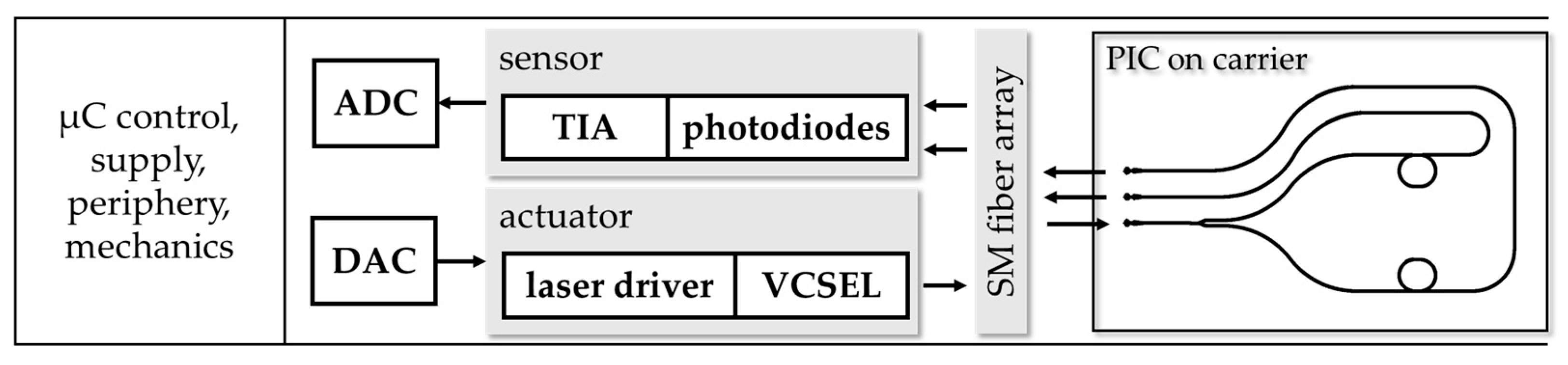
In order to demonstrate the suitability for point-of-care sensor applications, a portable system demonstrator has been constructed. This system requires a position-adjustable fiber array for initial PIC coupling optimization. Once calibrated, the system operates with subsequent chips without further adjustments to its miniaturized translation stages. In addition to the mechanical components, the demonstrator also contains integrated optoelectronics and electronics. This includes a driver circuit for the tunable vertical-cavity surface-emitting laser (VCSEL), receiver photodiodes with a transimpedance amplifier (TIA) stage, and a microcontroller for monitoring the effective coupling between the single-mode fiber array and the integrated waveguides. The corresponding signal chain is illustrated in
Figure 4. The selected VCSEL (BW10-1550-T-P from Bandwidth10 Inc., Berkeley, CA, USA) operates within the C-band wavelength range and maintains a low power output of less than 1 mW, classifying it as a Class 1 laser under the DIN EN 60825-1:2022-07 standard [
24]. From a safety perspective, this classification confirms that the laser is safe for long-term intentional exposure without causing harm to users.
The demonstrator shown in
Figure 5 measures approximately 150 mm by 150 mm by 200 mm. The operation of it can be seen in [
25]. The majority of the housing is made of synthetic resin. Aluminum components are used to provide structural stability. Both resin and aluminum have non-hazardous properties. However, to ensure the device is fully prepared for the market, particularly for use by individuals without specialized training, enhancements in user and product safety are required. This will involve efforts to meet the stringent safety standards expected of consumer products. Additionally, the materials chosen for the device must not only be chemically stable but also biocompatible when necessary [
26]. They must withstand solvent disinfection and sterilization processes without degrading, to ensure the device can be safely reused in environments where sterility is critical [
27]. For potential medical applications, future evaluations will need to verify the compliance with Food and Drug Administration (FDA) or Medical Device Regulation (MDR) regulations, ensuring the device meets all necessary guidelines.
4. Results and Discussion
4.1. Optical Characterization of Highly Tolerant Grating Coupler Structures
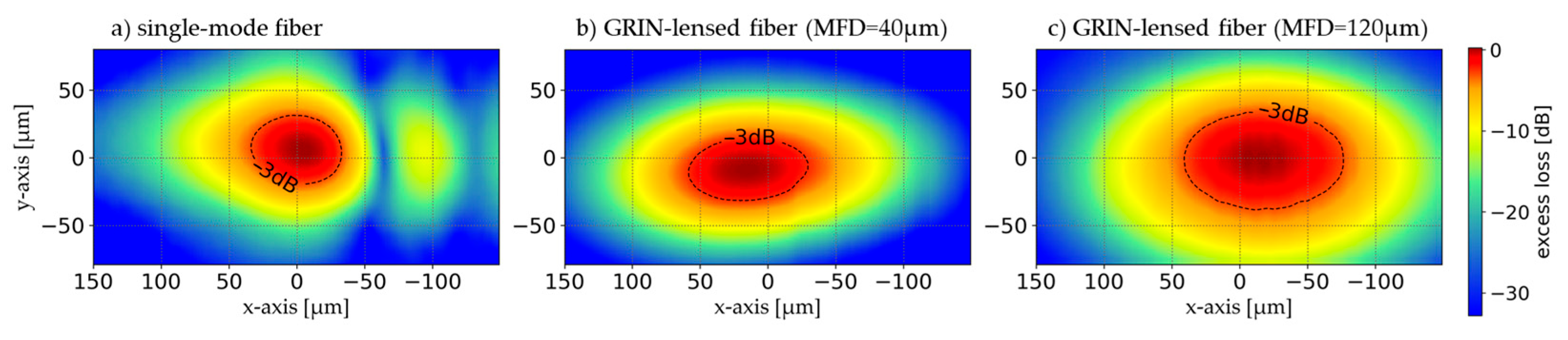
To explore the fiber-grating coupler interface, we examined both standard single-mode fibers and gradient index (GRIN) lensed fibers. GRIN-lensed fibers are beneficial for coupling single-mode waveguides to grating couplers, as they allow for precise beam shaping, which is crucial for maximizing coupling efficiency and minimizing sensitivity to misalignments [
28].
Transmission measurements were conducted by scanning the grating coupler surface with different fiber types. The lensed fibers included one with a 40 µm mode field diameter (MFD) for a collimated beam and another with a 120 µm MFD. In contrast, the also-tested standard single-mode fiber without lens (Corning SMF-28 Ultra fiber) features an MFD of 10.4 µm. The intensity distributions are illustrated in
Figure 6.
Table 2 lists the values for the 3 dB coupling tolerances in the lateral and longitudinal direction. It is important to recognize that the observed results are a convolution of the mode fields of the fiber and the grating coupler, pointing to their combined effect on the system performance.
The results indicate that the 3 dB coupling tolerance improves with an increase in the MFD of the fiber. However, this observation is nuanced by the spot radius of the grating coupler structure, which achieves the lowest absolute attenuation with the lensed fiber with MFD = 40 µm. The insertion loss (IL) for the tolerant grating coupler at a wavelength of 1550 nm and optimized central coupling was measured with IL = −6.2 dB (best value). A trade-off is necessary between a lower transmission with a higher coupling tolerance and a higher transmission with a lower coupling tolerance. Additionally, the spectral 3 dB bandwidth of the grating coupler structure was determined to be 25.5 nm.
Investigations akin to those of the grating coupler presented herein have been previously conducted, as documented in [
13,
14], but utilizing a silicon-on-insulator (SOI) material. The study in [
13] demonstrated a 3 dB alignment tolerance using GRIN-lensed fibers characterized by lateral and longitudinal tolerances of 34 µm and 21 µm at the 1550 nm wavelength, respectively. Details on the absolute insertion loss IL were not published. Furthermore, [
14] reported an alignment tolerance at a wavelength of 1300 nm of ±30 μm within a 1 dB threshold by employing a micro-lens integrated on the PIC as well as on the fiber array. This configuration achieved an insertion loss of 1.7 dB (best value). Neither study provided information on the spectral 3 dB bandwidth.
For optimal coupling efficiency, future development should focus on eliminating the asymmetry in the radial coupling tolerance. This could be achieved by adjusting the grating fill factor to adapt the emitted profile to more closely resemble a Gaussian intensity distribution [
29,
30]. Should lensed arrays be considered for use, the grating design could be modified to focus the light to match the lens MFD above it in a specified working distance [
30].
Lensed fiber arrays were excluded from subsequent experiments involving the integration of grating couplers with the passive positioning system due to their incompatibility with the cost constraints of point-of-care and disposable applications. In addition, the system with standard single-mode fiber arrays also has a sufficiently high coupling tolerance to support the optomechanical coupling. A key innovation of this work is the elimination of additional micro-lenses or gradient index lenses, while still achieving comparable alignment tolerance results.
4.2. Passive Positioning System Evaluation
Following the initial characterization of the bare PICs, the performance of the assemblies is evaluated using the same measurement system described in
Section 2. The disposables undergo testing without a realignment of the fiber array when a new chip is placed into the ball-groove coupling system detailed in
Section 3.
Therefore, a predefined quality criterion was used to sort out disposable chips that do not meet these key performance indicators (KPIs). The chosen KPIs are the modulation depth and the insertion loss at around 1550 nm. Given the characteristics of the tunable VCSEL used as the light source, only peaks around the 1550 nm wavelength can be effectively monitored by the miniaturized sensor system and these peaks must be significantly distinguishable from the background noise. In applications that employ MRR-based sensors, the imperative to minimize the on-chip propagation loss is notably less critical. The employed low-confinement waveguide designs result in higher propagation losses compared to other applications. Consequently, the PICs designed for these sensing applications differ significantly from the low-loss, high-confinement waveguide PICs commonly used in communication technologies.
Throughout the development phase of this research, it has been empirically determined that a minimum modulation depth of 8 dB is required and the insertion loss should not exceed −55 dB to ensure proper functionality. As a consequence, 33 out of 132 of the PIC assemblies were discarded for not meeting the KPIs, resulting in a production yield of 75%. The measured data for the entire PIC is summarized in the following
Table 3.
At a wavelength of 1550 nm, the modulation depths of the disposable chips are comparable to their initial characterization. This measurement outcome is consistent with expectations, as the modulation depth is primarily influenced by the design of the MRR and the MMI structures, rather than by the optical coupling efficiency of the grating couplers. The average optical loss at 1550 nm for these chips is 5.21 dB lower than what was achieved under initial active alignment conditions. The lowest transmission observed at the 1550 nm wavelength for the sorted chips is 49.9 dB. Consequently, it can be anticipated that all these chips will deliver reliable measurement results in the sensor system application without the need for a manual adjustment. Furthermore, the analysis revealed that the modulation depth of the MRR peaks at approximately a 1530 nm wavelength, not at 1550 nm as designed. The observed shift is presumably linked to variations in the stepper lithography process, which impacts the performance of the MMI coupler. However, the deviation in the process also affects the waveguides directly. The geometry of the MRR, the inherent resonator losses, and the coupling efficiency between the resonator and the bus waveguide are factors that contribute to this discrepancy. By refining the lithography process in a future iteration, the position of the maximum modulation depth could be optimized. Consequently, an average modulation depth of 19.92 dB (SD = 2.97 dB) and average insertion loss of 27.33 dB (SD = 2.39 dB) at the target wavelength of 1550 nm for the combined metrics of the coupling efficiency and on-chip waveguide losses were reproducibly achieved across a sample of N = 74 PICs, reflecting the combined metrics of the coupling efficiency and on-chip waveguide losses.
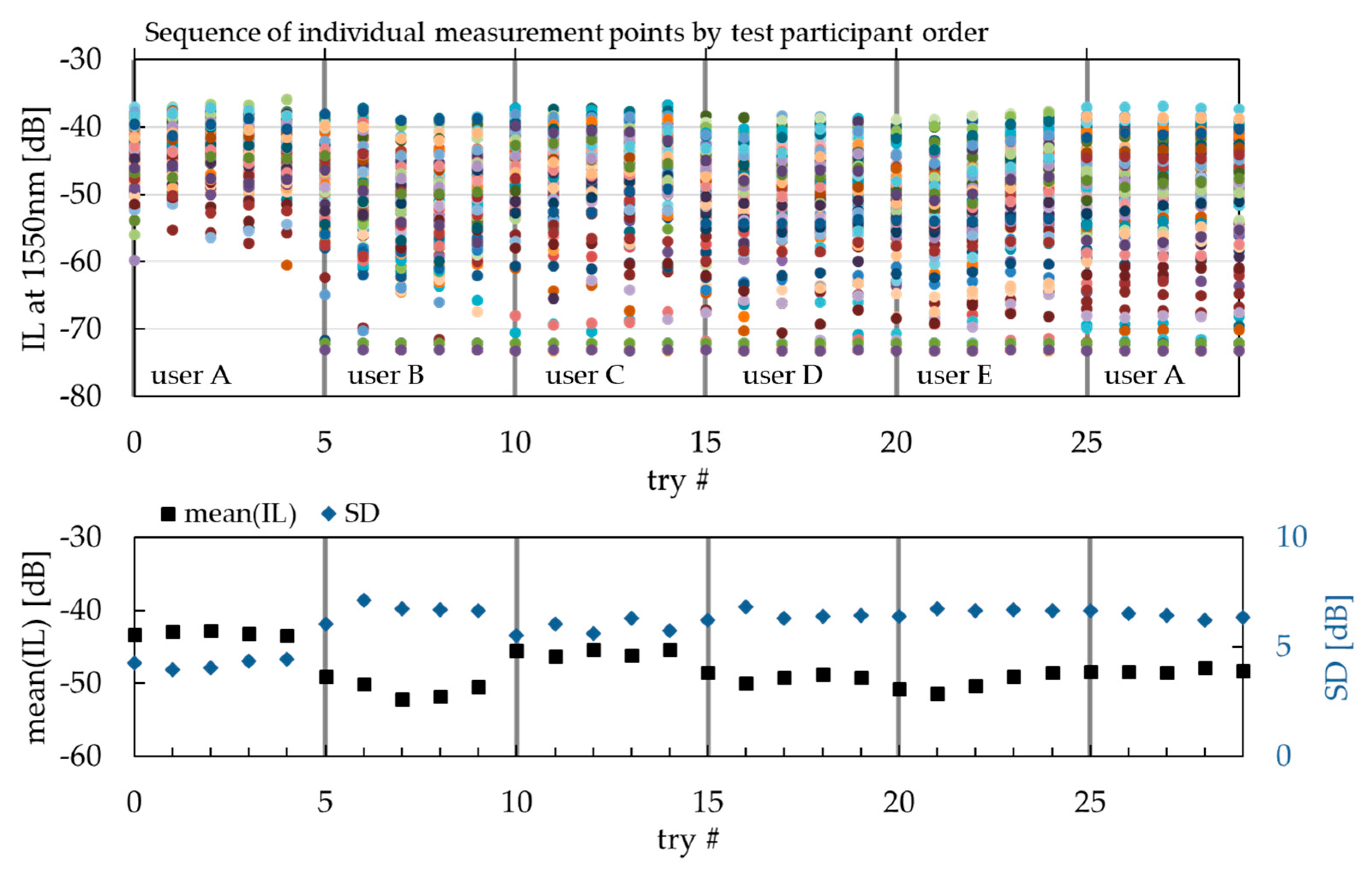
In order to better verify the characteristics of the mechanical kinematic coupling system, additional tests have been conducted. In this investigation, a standard single-mode fiber array (Corning SMF-28 Ultra fiber) without lenses is used. Emphasis is placed on the application of disposables intended for operation by untrained persons, which underlines a user-centered design approach. Usability testing was implemented to gather direct feedback on user–system interaction, thereby assessing the practicality of the developed passive coupling system. The durability of the disposables and the consistency of the coupling process were also tested within this experiment. A series of tests was performed where the PIC assemblies were clicked-in by five different individuals. Among these, one individual received training on the procedure, whereas the remaining four were novices. Each participant had the task of inserting the same 50 independent disposable chips into the system five times in a row. The testing sequence commenced with the trained participant, followed by the four untrained individuals, and concluded with a second session by the trained participant without calibrating the system in between, cumulatively generating 1500 test points. The coupling statistics were confirmed by evaluating the insertion loss, accounting for both on-chip losses and losses from the measurement system at the 1550 nm wavelength. The result is shown below in
Figure 7.
Out of 50 chips, 34 were successfully inserted into the developed coupling system 30 times each. Assemblies with an IL > −55 dB are deemed successful, given that a resonance frequency shift critical for sensor functionality can still be monitored. The data show that there is no significant difference whether trained or untrained personnel use the system. It was observed that the performance of user A was notably better during the first trial compared to the second. The chips that did not fail during the test show a maximum reduction of 9.4 dB in the IL for optical passive coupling, likely attributable to the mechanical wear and tear of the disposables during operation. An evaluation of the IL standard deviation (SD) shows an increase of the factor 1.8 (comparing the best versus worst SD values) across all chips per try number, with data from the failed chips excluded. The first two chips encountered failure during the fifth chip insertion (try #4) by user A. The failure rate throughout the testing is consistent and linear, with no single event causing multiple chips to fail simultaneously. For the best-performing individual chip, reproducibility with a SD of 1.8 dB was achieved. In contrast, ref. [
14] reported a significantly lower variability, documenting an SD of 0.2 dB in their lens-supported system across 30 insertion actions for an individual disposable. This discrepancy can largely be attributed to the lens system, which was intentionally excluded from our study, as the optical coupling strengths are sufficient for the application. This allows for reduced costs and system complexity.
The application of the developed repeatable passive fiber optic coupling system for single-mode waveguides in high-precision disposable photonic biosensors has thus been demonstrated.
4.3. Evaluation as Portable Photonic Sensor System
The aim is to ensure that the measurement system described in
Section 3 and depicted in
Figure 8 yields sensing results that are comparable to those obtained from the established stationary lab setup. Therefore, a randomly selected disposable assembly was used in the portable system. Subsequently, a chip from the same wafer batch was tested at the stationary measurement station for comparison.
To detect any shift in the MRR resonance wavelength due to a change in the effective refractive index in the sensor waveguide, the MRR surface was first moistened with distilled water. Following this, a 0.9% sodium chloride (NaCl) solution was applied to the chip using a pipette, while simultaneously recording the measurement signal with a sampling rate of 10 samples/s. The resulting data are presented in
Figure 9. For further details on the sensor MRR itself, including parameters like sensitivity and the limit of detection, please refer to [
10].
In summary, the measurement outcomes from both the stationary and portable setups are found to be comparable. The passive coupling of the assembled sensor chips, as discussed in previous sections, indicates that a resonance wavelength shift is measurable across all disposables. Notable differences include the slight variation in signal channels. These discrepancies can be attributed to the provisional method of liquid application. Initially, a precise drop of distilled water is placed on the sensor chip, which is subsequently mixed with a drop of NaCl solution during the measurement. The degree of mixing between the distilled water and the NaCl solution is not examined in detail in this study. To reduce the influence of these variables, it is essential to develop a microfluidic system tailored specifically for the setup, which will be addressed in future work. Such fluidic systems, as described in [
31], would enable precise control over the delivery and concentration of liquids to the sensor chip, ensuring more accurate and reliable results.
5. Conclusions
We have successfully fabricated and assembled 99 functional disposable sensor chips based on Si3N4 MRRs, optimized for the optical C-band. A key achievement is the development of a passive coupling system that allows these sensor chips to be interchanged without manual adjustments to the read-out-unit device, enabling the simple insertion and reliable coupling between device-side single-mode fibers and PIC-side grating coupler structures.
The robustness of this coupling system is underlined by two main factors: the chip-side optical coupler gratings that exhibit 3 dB tolerances of more than ±25 µm in the lateral and longitudinal directions, and the three-groove kinematic coupling design which ensures the precise passive alignment of the chip structure with the single-mode fiber in the µm range.
The system usability is enhanced by a magnet-guided snapping mechanism that positions the sensor chips opposite the optical sensor head. This feature is instrumental in facilitating the potential application of the sensor system in portable or wearable biosensing devices [
32,
33]. The straightforward manual insertion and magnetic fixation process, combined with the system tolerance for operation by individuals without specialized training, suggests its suitability for point-of-care scenarios. The assembly process of the sensor chips, which includes the PIC, carrier, and alignment structures, achieved a production yield of 75%. Additionally, this approach is also cost-effective since it obviates the need for integrating lenses or electro-optical components into the disposable unit. A usability assessment confirmed the system operational robustness, revealing an SD of 5.1 dB in insertion loss with N = 99 design-identical yet independent assembly units, without a realignment of the positioning system post-calibration. The passive coupling method proved to be consistent across multiple uses by various individuals, including those without prior training, indicating its readiness for practical applications. To our knowledge, prior demonstrations of repeatable passive coupling, as reported by [
14], were limited to employing the use of a single, individual disposable chip, rather than a series of multiple samples. The preliminary studies utilized a distinct material platform. In our investigation, the PIC is based on Si
3N
4 instead of SOI technology, as it is in [
13,
14]. Furthermore, our approach deliberately avoids additional lens systems, which were utilized in earlier developments. This exclusion reduces both the cost and complexity of the system. Additionally, a test measurement using a reference solution on the demonstration device indicated its potential functionality for biosensor technology.
However, the development of the system is not yet complete. There is potential for a further improvement in the quality of the output signal and the coupling tolerances by refining the design of the integrated photonic elements and the manufacturing process, with a focus on enhancing the spot radius and eliminating asymmetry in the radial coupling tolerances. Future work will investigate the feasibility of transitioning to an automated assembly process for the sensor chips, moving away from the current manual methods. The integration of the system with microfluidics [
31,
34] and the surface functionalization of the MRR sensors with capture molecules [
17] will be pursued to enable selective sensing capabilities.
In conclusion, this research introduces a reliable method for the passive coupling of single-mode waveguides with micron-level precision. This method is well-suited for high-precision disposable devices and signifies progress toward the broader application of photonic integrated sensors in point-of-care settings, particularly for chemical and biological analyses.

 ,
, 


