Article

High-Precision Semiconductor Substrate Thickness Gauge Based on Spectral-Domain Interferometry

Fujian Provincial Key Laboratory of Terahertz Functional Devices and Intelligent Sensing, School of Mechanical Engineering and Automation, Fuzhou University, Fuzhou 350116, China
*
Author to whom correspondence should be addressed.
Photonics 2024, 11(5), 422; https://doi.org/10.3390/photonics11050422
Submission received: 28 February 2024 / Revised: 8 April 2024 / Accepted: 29 April 2024 / Published: 1 May 2024

Abstract

:
The flatness of semiconductor substrates is an important parameter for evaluating the surface quality of semiconductor substrates. However, existing technology cannot simultaneously achieve high measurement efficiency, large-range thickness measurement, and nanometer-level measurement accuracy in the thickness measurement of semiconductor substrates. To solve the problems, we propose to apply the method that combines spectral-domain optical coherence tomography (SD-OCT) with the Hanning-windowed energy centrobaric method (HnWECM) to measure the thickness of semiconductor substrates. The method can be employed in the full-chip thickness measurement of a sapphire substrate, which has a millimeter measuring range, nanometer-level precision, and a sampling rate that can reach up to 80 kHz. In this contribution, we measured the full-chip thickness map of a sapphire substrate by using this method and analyzed the machining characteristics. The measurement results of a high-precision mechanical thickness gauge, which is widely used for thickness measurement in the wafer fabrication process, were compared with the proposed method. The difference between these two methods is 0.373%, which explains the accuracy of the applied method to some extent. The results of 10 sets of repeatability experiments on 250 measurement points show that the maximum relative standard deviation (RSD) at this point is 0.0061%, and the maximum fluctuation is 71.0 nm. The above experimental results prove that this method can achieve the high-precision thickness measurement of the sapphire substrate and is of great significance for improving the surface quality detection level of semiconductor substrates.

1. Introduction

With the rapid development of the semiconductor industry, this industry has increasingly higher requirements for the surface quality of semiconductor substrates [1]. The substrate is the base of the semiconductor devices; its surface quality has a great impact on the growth of epitaxial layers and the processing, preparation, and performance of chips and optoelectronic semiconductor devices [2,3,4,5]. The substrate flatness or total thickness variation (TTV), which is used to describe the thickness variation at various locations on the substrate, is one of the main indicators to evaluate the surface quality of semiconductor substrates [6]. In the fields of micro–nano processing and photolithography, the feature sizes are becoming smaller and smaller. When the feature size of photolithography reaches the nanometer scale, we will not be able to ignore the impact of the TTV on focusing during the photolithography processing. Exposure is a key step in photolithography processing; underexposure or overexposure will harm the pattern quality. If the TTV seriously exceeds the focal depth of the photolithography machine, the machine will become out of focus during the exposure process [7]. To achieve a higher yield, we must conduct the high-precision detection of the TTV of semiconductor substrates. On the other hand, a higher surface quality will provide a better foundation for the subsequent processing of semiconductor devices. More importantly, the high-precision full-chip thickness measurement of semiconductor substrates can not only directly reflect its surface quality, but also reflect problems such as an uneven substrate support plate and non-uniform force during substrate processing, and ultimately guide the improvement of processing methods [8].
Substrate thickness measurement techniques can be classified into contact and non-contact methods. Contact methods include the ultrasonic thickness measurement method [9], mechanical thickness measurement method, etc. These methods are prone to damage the surface when detecting ultra-thin substrates and substrates with high surface quality requirements. Therefore, non-contact methods are more suitable for the thickness measurement of these semiconductor substrates. The following will introduce several currently commonly used non-contact methods. The double-beam laser interferometer method is a method that uses a single-frequency laser as the probe light. This method obtains the thickness by collecting the interference intensity of the upper and bottom surfaces of the substrate. Its measurement accuracy and efficiency are relatively high, but the measurement range of this method usually only reaches the micron level [10]. The ellipsometry method obtains the thickness by detecting changes in the polarization state of the reflected light from the sample. Since the polarization state of the reflected light is highly sensitive to thickness changes, this method has nanometer-level measurement accuracy, but its measurement range usually only reaches a few microns. More importantly, since each measurement needs to be changed by a series of parameter conditions, the measurement efficiency of this method is low [11]. The laser triangulation method is a common non-contact thickness measurement method. The measurement principle of this method is to use a laser to illuminate the substrate surface and the reference plane at a certain angle, and then use a photodetector to measure the offset of the reflected light on the two planes, which is proportional to the thickness of the substrate. This method can reach a centimeter-level measurement range and has high measurement efficiency, but it can only achieve micron-level measurement accuracy [12]. The spectral confocal method utilizes the dispersion phenomenon of broadband light when passing through the lens. This method uses a dispersive lens to separate different wavelengths of light on the optical axis. When the light source is focused on the sample through the dispersive lens, different interfaces of the sample will reflect different wavelengths of light. We can calculate the sample thickness by detecting the wavelength of reflected light. This method has a millimeter-level measurement range, high measurement efficiency, and can reach nanometer-level measurement accuracy. However, this method belongs to intensity detection. When measuring non-highly transparent material, there is a problem in that the light intensity rapidly attenuates, and the signal is difficult to accurately analyze [13].
To achieve high measurement efficiency, large thickness measurement, and nanometer-level measurement accuracy at the same time, this paper proposed to use spectral-domain optical coherence tomography (SD-OCT) combined with the Hanning-windowed energy center correction method (HnWECM) for the thickness measurement of semiconductor substrates. SD-OCT is a high-precision three-dimensional tomography technology based on the principle of low-coherence interference. This technology uses broadband light to detect the sample and obtains its internal structure information by analyzing the interference signals generated by the coupling of the detected beam and reference beam. Compared with the intensity detection method, this method has a higher signal-to-noise ratio, and the interference method can amplify weak signals, so this method is widely used in biomedicine, industrial non-destructive testing, and other fields. SD-OCT technology belongs to the second-generation version of optical coherence tomography technology. It relies on high-speed linear array charge-coupled devices (CCDs). The frame rate of the CCD is as high as tens of thousands of Hz. It has extremely high single-point measurement efficiency in thickness measurement. Therefore, this is a high-efficiency non-destructive testing method, and it has a millimeter-level measurement range, which can meet the thickness measurement needs of most semiconductor substrates [14]. Combined with the HnWECM method, this technology can achieve nano-scale measurement accuracy, which was validated in our previous work [15].
Sapphire ( α - Al 2 O 3 ) substrates have excellent properties such as high hardness, high melting point, good light transmittance, good thermal stability, and stable chemical properties. Therefore, it is widely used in manufacturing semiconductor substrates, optical windows, etc. In the semiconductor lighting industry, it has become the most suitable substrate material for manufacturing light-emitting diodes [16]. In this work, we took a sapphire substrate as the example to research substrate thickness measurement.

2. Measurement Principles and Methods

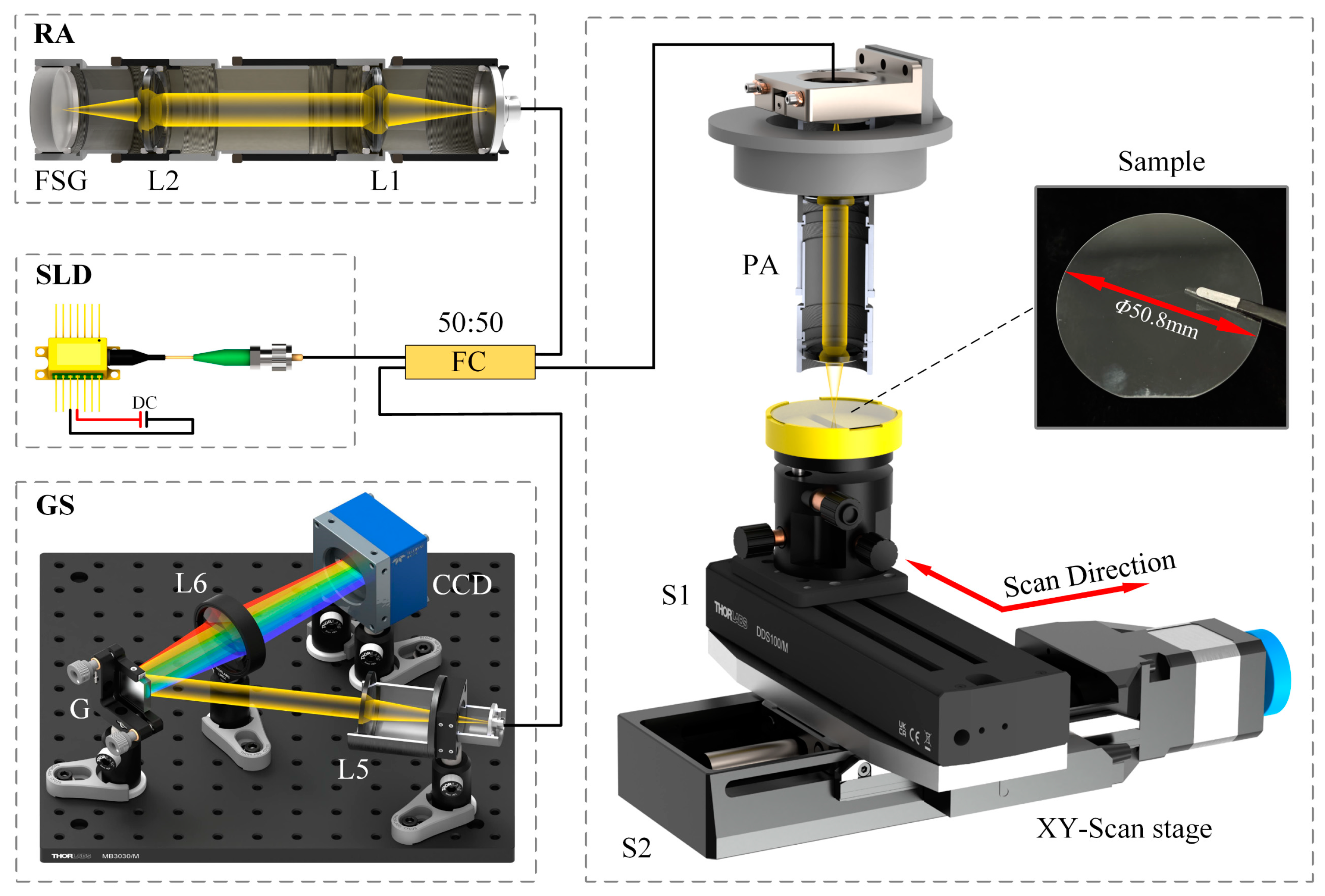
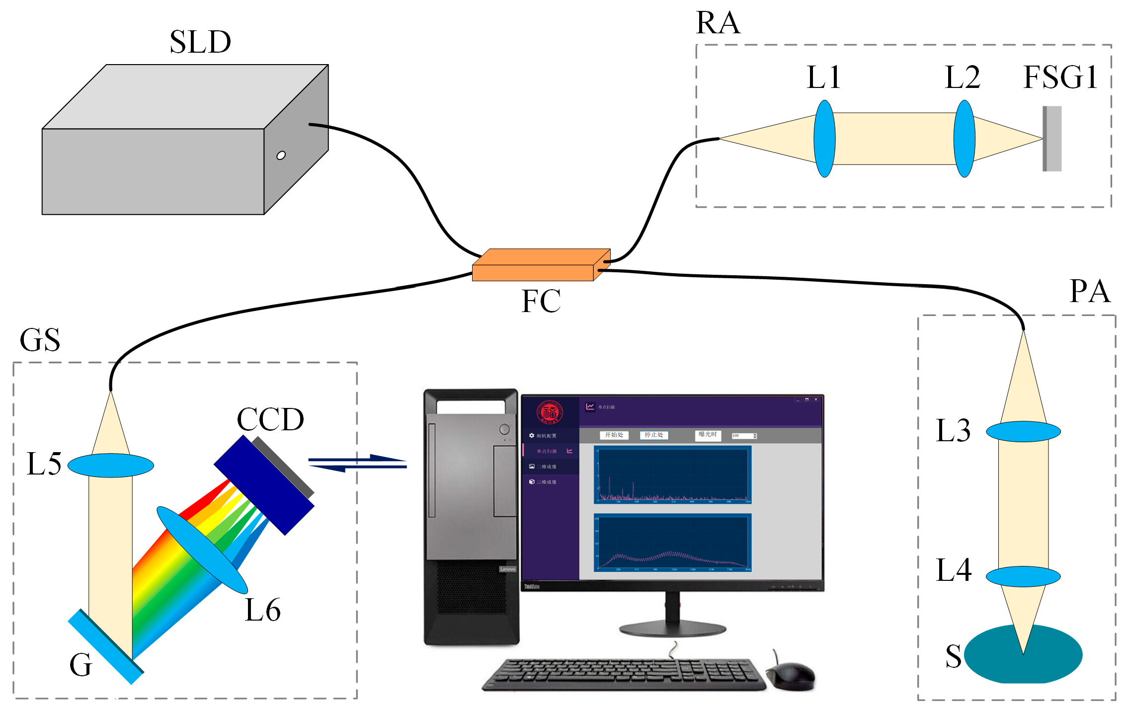
In our work, we use SD-OCT technology to measure the full-chip thickness of the sapphire substrate. Figure 1 shows the schematic diagram of fiber-optic SD-OCT system. The system consists of a super luminescent diode (SLD), fiber coupler (FC), probe arm (PA), reference arm (RA), grating spectrometer (GS), and computer.
The broadband light emitted by the SLD is divided into probe light and reference light by the fiber coupler. The reference light is collimated into parallel light by lens 1 (L1) and then focused on the upper surface of the fused silica glass 1 (FSG1) by lens 2 (L2). Then, the reference light will be reflected to the FC carrying the optical path information of the upper surface of the FSG1. Similarly, the probe light will return to the FC carrying the optical path information of the upper and bottom surfaces of the sapphire substrate. Here, the difference between the optical length from FC to FSG1 and the optical length from FC to S is within the interference range. Since the SLD has extremely high spatial and temporal coherence performance, the interference will occur when the returned probe light and reference light gather in the FC. Finally, the interference signal is collected by the GS and processed by the computer. Ignoring the scattering of the probe light in the sample, the interference spectrum of the probe light and the reference light can be expressed as follows:
I k = S k ( E R 2 + 2 E R + a z cos k 2 z d z   + + + a z a z exp i k 2 z z d z d z )
where k is the wavenumber, S k is the spectral density function of the light source, E R is the amplitude of the reflected reference light, a z is the amplitude of the reflected probe light at depth z , 2 z is the optical path difference (OPD) between the reference light and the probe light at depth z , and 2 z is the OPD of the probe light between depth z and depth 2 z z . In Equation (1), the first part is the self-coherence term of the reference light, and the second part is the mutual interference term between the reference light and the probe light reflected from different layers of the sample. The third part is the self-interference term between each layer of the sample.
A double-sided polished sapphire substrate was used as the measurement sample. The probe light is mainly reflected by the upper and bottom surfaces of the sapphire substrate. The interference between the reference light and the probe light reflected by these surfaces and the self-interference of the upper and bottom surfaces of the sapphire substrate are the main components of the interference spectrum. Thus, we can further simplify Equation (1) to the following:
I k = S k E R 2 + 2 E R a z u p cos k 2 z u p   + 2 E R a z d o w n cos k 2 z d o w m   + a z u p a z d o w n cos i k 2 z d o w n z u p
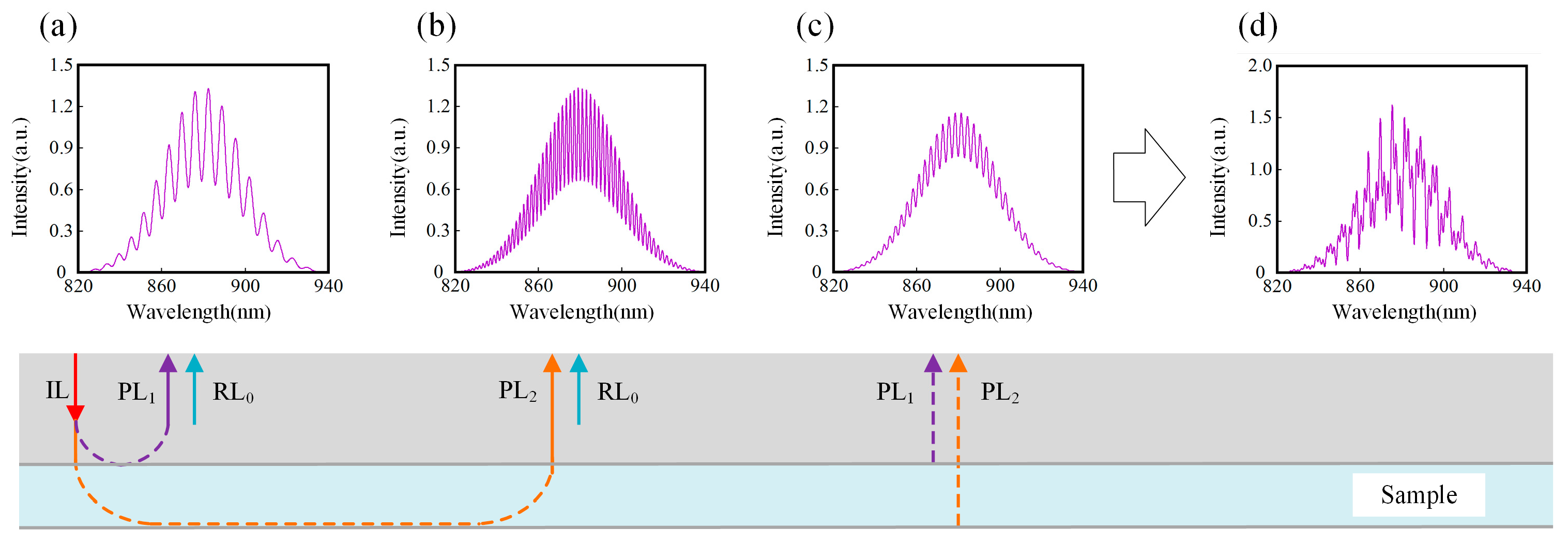
where z u p is the OPD between the probe light reflected from the upper surface of the sapphire substrate and the reference light, and z d o w n is the OPD between the probe light reflected from the bottom surface of the sapphire substrate and the reference light. In Equation (2), the first term is the DC term, and the second term is the interference spectrum between the reference light and probe light reflected from the upper surface of the sapphire substrate, as shown in Figure 2a. The third item is the interference spectrum between the reference light and the probe light reflected from the bottom surface of the sapphire substrate, as shown in Figure 2b, and the fourth item is the interference spectrum between the probe light reflected from the upper surface and the bottom surface of the sapphire substrate, as shown in Figure 2c. Finally, the interference spectrum we collected by the GS is the result of adding up the above parts, as shown in Figure 2d.
The depth position information of different surfaces of the sapphire substrate is expressed as different OPDs between the reference light and the probe light. These OPDs are reflected in the interference spectrum as cosine components of different frequencies. Thus, we can calculate the physical thickness of the sapphire substrate by decoding the frequency of each component of the interference spectrum. Typically, one decodes these frequency components by performing the FFT on the interference spectrum, converted to the wavenumber domain. The FFT result of the Equation (2) can be expressed as follows:
F F T I k = F F T S k E R 2 δ z 0   + 2 E R a z u p δ z z u p + δ z + z u p   + 2 E R a z d o w n δ z z d o w n + δ z + z d o w n   + a z u p a z d o w n δ z z u p + z d o w n + δ z + z u p z d o w n = A B + C + D + E
where A is the FFT result of the spectral density function of the light source, ⊗ represents the convolution symbol, A ⊗ C, A ⊗ D, and A ⊗ E, respectively, represent the interference spectrum’s FFT results of the upper surface, bottom surface, and between the upper and bottom surfaces of the sapphire substrate.
The axial resolution and lateral resolution of the SD-OCT system can be calculated using the following equations:
Δ z = 2 ln ( 2 ) π λ 0 2 Δ λ
Δ x = d f L 4 f L 3
where λ 0 and Δ λ represent the central wavelength and spectral bandwidth of the light source, d signifies the size of the input beam spot, f L 4 and f L 3 stand for the focal length of the focusing lens and collimating lens in the probe arm.
To accurately decode the position information of all surfaces, we need to perform further data processing on the interference spectrum. Since the GS collects the interference spectrum signal in the wavelength domain, the periodic intervals of the interference signal are nonlinear, which will cause spectrum broadening in the FFT results. Therefore, we need to perform a coordinate transformation of the interference spectrum signal from the wavelength domain to the wavenumber domain. After this operation, we will obtain the interference signal whose period intervals tend to be equal, as shown in Figure 3a,b. Finally, we perform FFT operations on the interference spectrum signal after coordinate transformation and use the HnWECM method to accurately obtain the position values of each surface of the sapphire substrate. Figure 3c shows the FFT result of the interference spectrum signal.
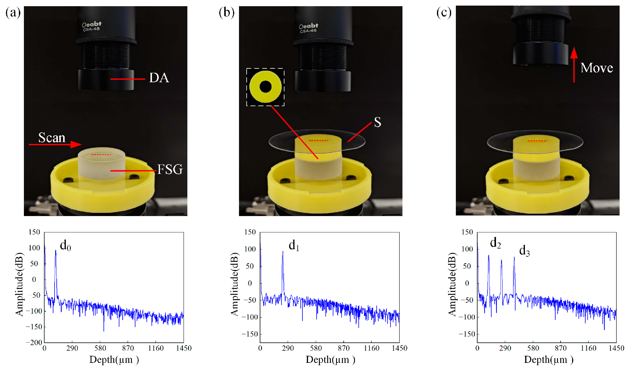
For broadband lights, the group refractive index is defined as the ratio of the group velocity of light in a vacuum and the one in a medium (group velocity refers to the propagation velocity of energy and information in the medium). It is a parameter related to the refractive index and dispersion of the medium [17]. In the broadband optical interference system, the group refractive index parameter is used to describe the relationship between the optical path and the actual distance. To calculate the physical thickness of the sapphire substrate, we also need to measure the group refractive index of the sapphire substrate. We used the fiber-optic SD-OCT system to conduct three sets of experimental measurements on the sapphire substrate [18]. Firstly, we place the fused silica glass FSG near the focus of the probe light, as shown in Figure 4a. In this condition, the upper surface of the FSG is within the measurement range of the system. We collect the first set of interference spectrum signals and perform data processing on it to obtain the positions of the upper surface of the FSG. Secondly, we keep the position of the FSG unchanged and place the sapphire substrate above the FSG at a certain height, as shown in Figure 4b. The upper and bottom surfaces of the sapphire substrate are outside the measurement range of the system. The system cannot obtain the upper surface and bottom surface positions of the sapphire substrate. However, because the refractive index of the sapphire substrate is different from the refractive index of air, inserting the sapphire substrate will introduce additional optical path length. This will increase the OPD between the reference light and the probe light that returned from the upper surface of the FSG. At this time, we collect the second set of interference signals and perform data processing. We will obtain the FSG upper surface positions after inserting the sapphire substrate. Finally, we move the probe arm up a certain distance so that the sample is within the measurement range of the system, as shown in Figure 4c. At this time, we collect the third set of interference spectrum signals and process it. We obtain the bottom surface and upper surface positions of the sapphire substrate. To reduce measurement errors caused by environmental vibration, etc., we need to collect multiple sets of data, calculate the average of each surface position, and calculate the group refractive index of the sapphire substrate using the following equations:
d = d 3 d 2 d 1 d 0 n air n s = d 3 d 2 d
where n s is the group refractive index of the sapphire substrate, and n air is the standard atmospheric refractive index under the current experimental environment. After obtaining the group refractive index, we also need to calculate the final sample thickness by the following equation:
T = z u p z d o w n n s

3. Experiment and Results

3.1. Experimental System and Group Refractive Index Measurement

The experimental device is shown in Figure 5. The system light source uses a SLD with a central wavelength of 884 nm and a bandwidth of 97 nm (SLD, EXS210088-02, Exalos Inc., Schlieren, Switzerland), The RA is composed of the L1 (f = 25 mm), L2 (f = 50 mm), and fused silica glass FSG (L1, LB1757, Thorlabs Inc., Newton, NJ, USA; L2, LB1027, Thorlabs Inc., Newton, NJ, USA; FSG, PF10-03, Thorlabs Inc., Newton, NJ, USA). The lenses used by the PA are the same as those of the RA, and the above optical components are installed in an optical sleeve with a diameter of 25.4 mm. The splitting ratio of the FC is 50:50 (FC, TW850R5A2, Thorlabs Inc., Newton, NJ, USA). The parts of the system are connected by a single-mode FC, and the spot size of the light emanating from the single-mode fiber is about 5 μm. The theoretical value of the system’s axial resolution Δ z is 4.044 μm and lateral resolution Δ x is 10 μm, as calculated by Equations (4) and (5). The GS used in the system consists of the L5 (f = 60 mm) and L6 (f = 100 mm), a grating G (1200 lines/mm) (G, GR25-1208, Thorlabs Inc., Newton, NJ, USA), and a linear array CCD camera which has 2048 pixels and the maximum line frequency can reach 80 kHz (CCD, LA-GM-02K08A, DALSA Inc., Waterloo, ON, Canada). The sample scanning device of the system is an XY-axis linear scanning stage. The sample is placed on the scanning stage through a special fixture. The scanning stage consists of a high-speed linear displacement stage S1 and a low-speed linear displacement stage S2. The movement stroke of S1 is 100 mm and its maximum speed can reach 500 mm/s (S1, DDS100/M, Thorlabs Inc., Bergkirchen, Germany). The movement stroke of S2 is 150 mm, and the repeatable positioning accuracy can reach 100 nm (S2, PLS-85, Physik Instrumente Inc., London, UK).
Due to experimental environment influences, the actual resolution of the system may not reach the theoretical resolution. We will conduct two experiments to test the actual resolution of the system. For experimental resolution, we test the axial resolution of the system by measuring the number of periods at three different positions, and the lateral resolution is determined by measuring a resolution test target. The axial resolution testing experiment utilized a linear motorized stage (PLS-85, Physik Instrumente Inc., London, UK) to move the FSG in the reference arm. The motorized stage is controlled to move the FSG to three different positions with intervals of 500 μm between each pair. The number of periods of the interference signal are recorded at each position. Five repeated experiments were conducted, and the results are shown in Table 1.
By dividing the distance between two positions by the corresponding number of periods, we can obtain the actual distance corresponding to each period, which represents the axial resolution of the system. Three axial resolutions can be calculated from the three positions. The average of these three resolution results will be taken as the axial resolution result for one experiment. The average of the results from the five repeated experiments is 4.267 μm, which is taken as the experimental axial resolution of the system.
The lateral resolution testing experiment involves using the system to measure a resolution target (R3L3S1N, Thorlabs Inc., Newton, NJ, USA). The lines in the results begin to blur in the sixth element of group 5. According to the official data sheet, the experimental lateral resolution of the system is greater than 9.84 μm and less than 8.77 μm.
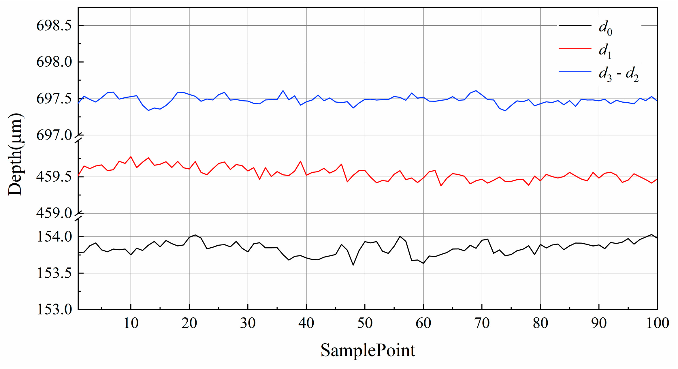
According to the method described previously, we first measured the group refractive index of the sapphire substrate. To reduce experimental errors, we needed to collect multiple points of data for calculation. We chose a straight line with a length of 500 microns near the center of the sapphire substrate for measurement. A total of 100 points were collected on this straight line, and the interval between points was 5 µm. For each point, we conducted three sets of measurement experiments according to the method in the previous section. The calculation results of d 0 , d 1 and d 3 d 2 of 100 collected points are shown in Figure 6. The mean values of d 0 , d 1 and d 3 d 2 are 153.848 µm, 459.551 µm, and 697.483 µm, respectively. Then, we put the above calculation results into Equation (6) to calculate the group refractive index of the sapphire substrate n s , which is 1.780.

3.2. Full-Chip Thickness Measurement and Repeatability Experiments

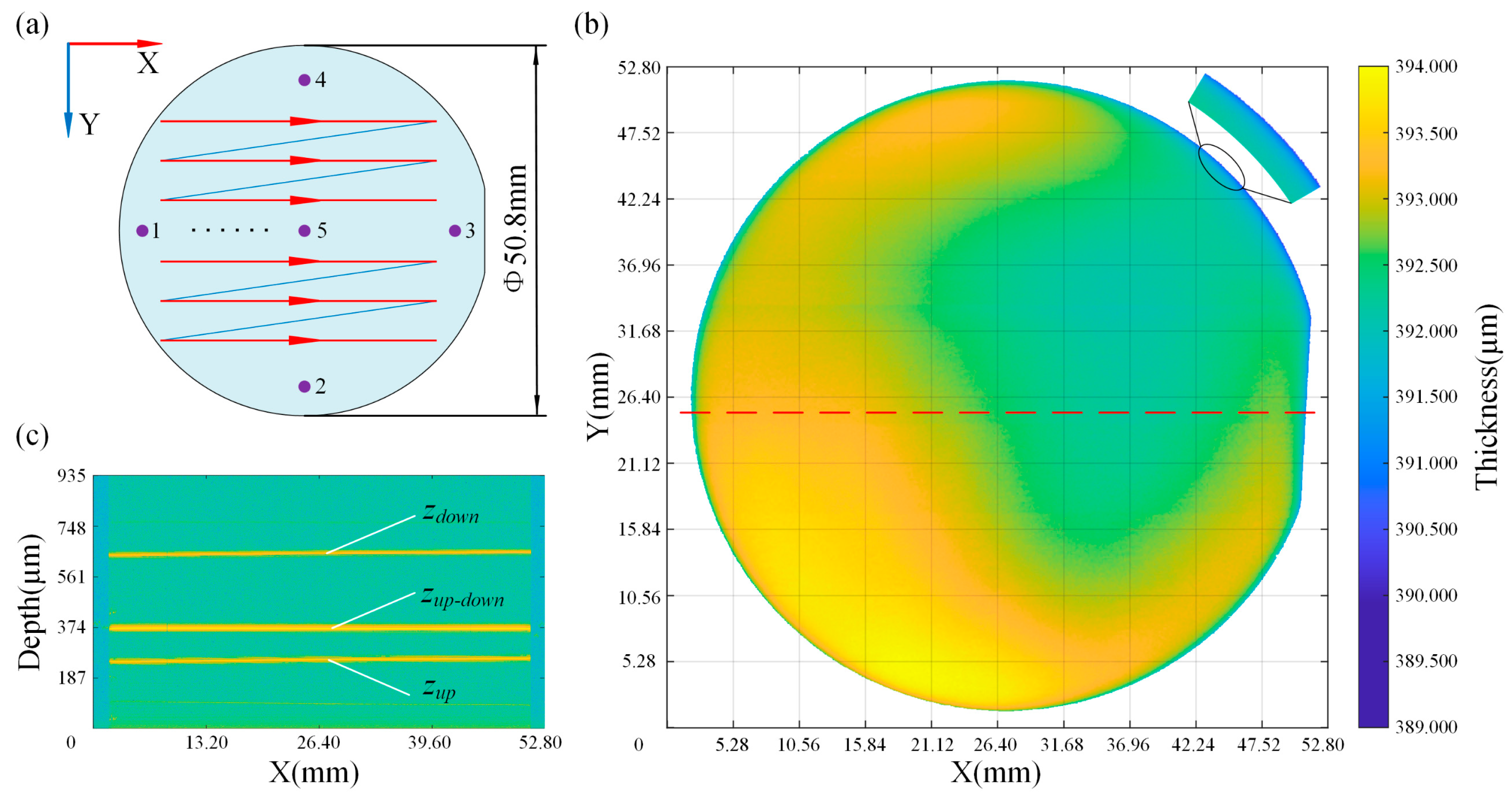
Using the above experimental system and the calculated group refractive index, we measured the full-chip thickness map of the sapphire substrate. The scanning device consists of two linear displacement stages. The displacement stage S1 is driven by a brushless DC motor. Its maximum speed can reach 500 mm/s, which can achieve fast scanning. In the experiment, the displacement stage performed X-direction scanning. After each X-direction scan is completed, the displacement stage S2 moves a certain distance in the Y-direction, and the scanning path is shown in Figure 7a. The diameter of the sapphire substrate used in the experiment is 50.8 mm. The scanning lengths in the X and Y directions are both 60 mm. The intervals between sampling points in the X and Y directions are both 40 µm. The group refractive index of the sapphire substrate n s is 1.780. The full-chip thickness map of the sapphire substrate is shown in Figure 7b. Experimental results show that the average thickness of the sapphire substrate is 392.832 µm, the maximum thickness is 393.993 µm, and the minimum thickness is 389.937 µm. The overall uneven thickness observed is attributed to the processing techniques of the sapphire substrate material. We will provide a more detailed explanation in the discussion section.
To verify the accuracy of the experimental results, we used a high-precision mechanical thickness gauge (C640, Labthink International Inc., Jinan City, China), which is commonly used in the semiconductor substrate production industry, to measure the five positions shown in Figure 7a. The resolution of the C640 is 100 nm, the measurement range is 0–2 mm, and its detection head is a cylindrical surface with a diameter of 8 mm. Therefore, its measurement results can be regarded as the average thickness within this range. To reduce the experimental error, we measured the above five measurement positions three times and used the average of the three measurements as the final thickness at that position. Similarly, we measured the average thickness of the above five positions within a diameter range of 8 mm based on the full-chip thickness map obtained by our method. The results of the two measurement methods are shown in Table 2. The average thickness measured using the thickness gauge is 394.51 µm, and the average thickness measured using our method is 393.040 µm. The difference between the two methods is 0.373%. While this result may not prove that our method has achieved nanometer-level precision, it does to some extent demonstrate the accuracy of our method.
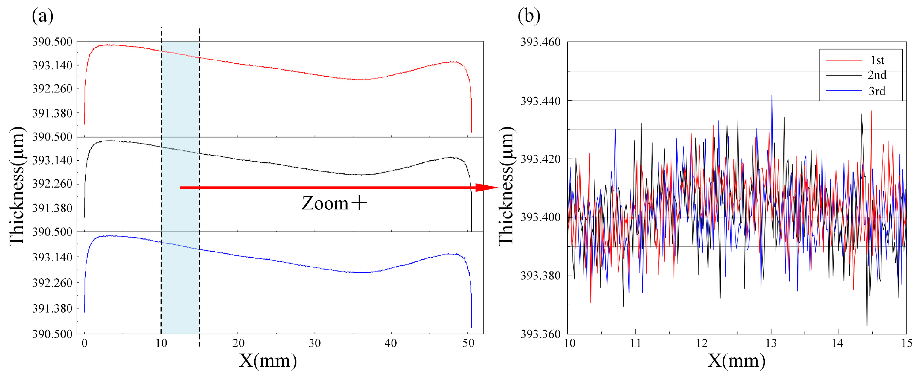
To verify the repeatability accuracy of our method, we conducted 10 sets of repeated measurements along the same straight path along the diameter of the sapphire substrate (indicated by the red dashed line in Figure 7b). The sampling point interval for each measurement is 20 µm. Figure 8a shows the measurement results of three sets of data among the ten sets of data, and Figure 8b is a partial enlargement of the 10–15 mm range. From Figure 8b, it can be concluded that the result fluctuates within 60 nm.
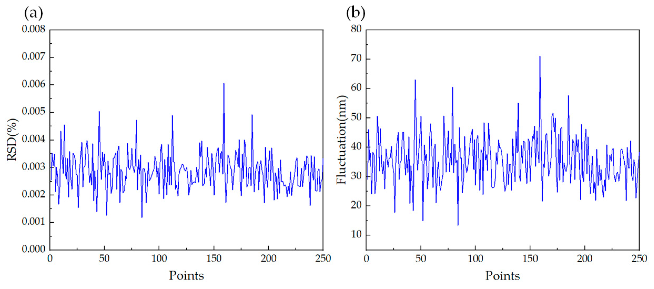
We evaluated the repeatability of our method by calculating the standard deviation of 250 measurement points within the 10–15 mm range of 10 sets of data. The relative standard deviation (RSD) and fluctuation for each test point across 10 sets of data are illustrated in Figure 9. Among them, the maximum RSD is 0.0061%, the minimum is 0.0012%, and the average is 0.0029%. The maximum fluctuation is 71.0 nm, the minimum fluctuation is 13.4 nm, and the average is 35.7 nm. This result proves that our method has high repeatability accuracy when measuring the thickness of the sapphire substrate. Moreover, by enhancing the power of the light source and reducing the noise of the spectrometer, among other methods, the signal-to-noise ratio of the system can be improved, thereby further enhancing system stability.

4. Discussion

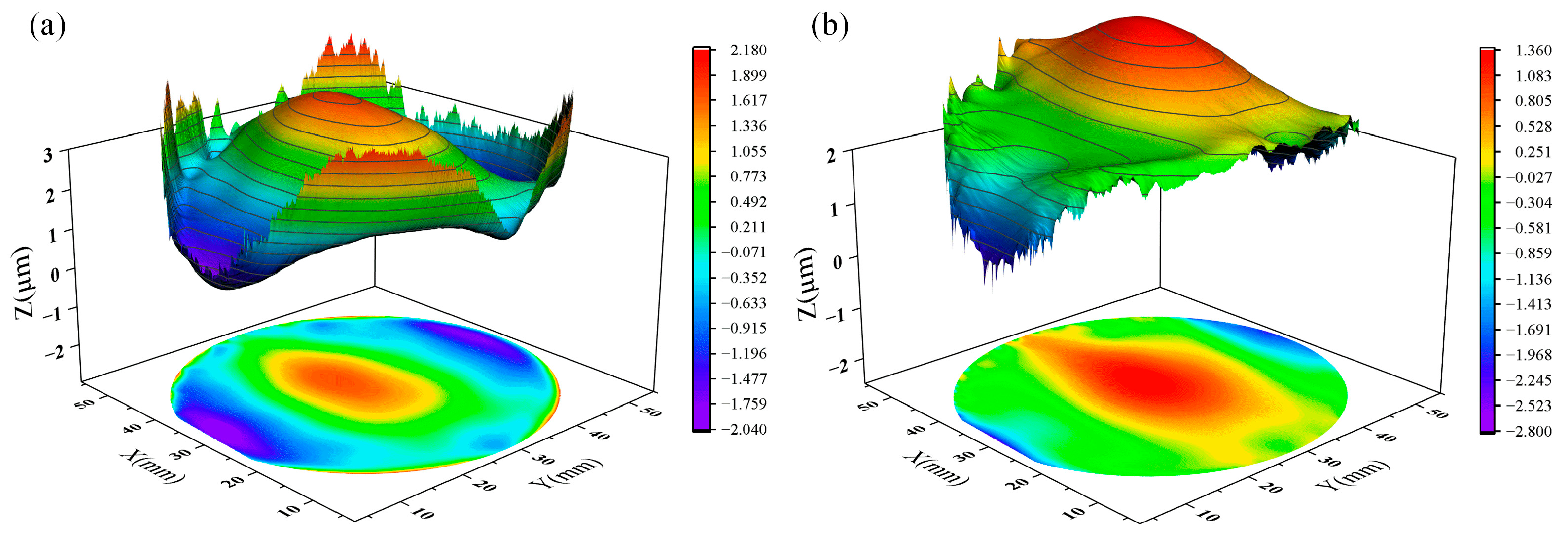
From the full-chip thickness map in Figure 7b, we can observe the unevenness of the sapphire substrate and some features caused by processing. By analyzing these features, we can target and solve the problems that exist in substrate processing. In Figure 7b, for example, we can observe that the bottom left part of the substrate is significantly thicker than the upper right part. Since the measurement method used in this paper is to obtain the thickness of the sample by the difference between the absolute positions of the upper and bottom surfaces of the sapphire substrate, we can easily obtain the three-dimensional morphology of the upper and bottom surfaces of the substrate with nanometer precision from the measurement data, as shown in Figure 10. This figure allows us to analyze the substrate thickness distribution and processing characteristics more intuitively.
The sapphire substrate’s saddle-shaped thickness distribution is primarily due to the lack of cutting ability of diamond wire saws during the pre-slicing process, which causes the processing of residual stress to be larger and ultimately shows a saddle-shaped face shape. During the grinding stage, as the thickness of the substrate material removal increases, the shape of the substrate surface should gradually change from a saddle-shaped to concentric circle-shaped thickness distribution, which is thicker in the middle, and thinner around the edge. Uneven pressure exerted by the grinding disk on the substrate during the grinding process and insufficient grinding time may lead to the saddle-shaped surface topography shown in Figure 10. At the same time, we can also observe that the thickness of the sapphire substrate is thinner at the edge. This is because when grinding the substrate, the abrasive liquid is more likely to enter the edge part of the substrate, resulting in a greater material removal rate at the edge of the substrate. On the other hand, the grinding fluid cannot easily enter the middle of the substrate, resulting in a smaller material removal rate in the middle of the substrate. This ultimately results in a substrate with features that are thicker in the middle and thinner at the edges [19].
From the calculation results in Table 2, we can see that there are certain differences between the results measured using our method and the C640. We analyze the reasons for this difference in the following ways. First of all, the C640 is a contact detection instrument. It determines whether it can start measuring the thickness of the sample by monitoring the pressure exerted by the detection head on the sample. Samples of different materials will have different deformations under the same pressure standard, which may lead to final measurement errors. On the other hand, our method uses optical measurement methods. The thickness we obtain is most accurate when the optical axis of the incident light is completely perpendicular to the sample plane. The angle between the optical axis of the probe light and the sample plane will change the thickness we measure. Although we designed a special sample fixture in the experiment to adjust the angle between the sample plane and the optical axis of the probe light, there is still a certain error due to the mechanical adjustment device. This is also the main reason for the difference between our measurement results and C640. Finally, another main reason for the measurement difference is environmental vibration. Since optical-based methods have a certain sensitivity to environmental vibrations, the vibrations of the environment will be reflected in our measurement results to a certain extent. However, we can reduce the measurement error caused by environmental vibration as much as possible by taking active or passive vibration isolation methods.
5. Conclusions

In the present work, we took the sapphire substrate as an example to study the application of the SD-OCT system and the HnWECM method in semiconductor substrate thickness measurement. We analyzed the features on the sapphire substrate thickness cloud map from a processing perspective. Compared with the measurement results of the high-precision mechanical thickness gauge C640, the difference between the two methods is 0.373%. This result proves the accuracy of our applied method to some certain extent. The results of multiple measurement experiments show that the maximum RSD is 0.0061%, and the maximum fluctuation is 71.0 nm. The results may have been affected by environmental factors during the experiment, such as vibration and Abbe error. The above experimental results prove that the method used in this article can achieve ultra-high-precision semiconductor substrate thickness measurement and is expected to become a novel high-precision semiconductor substrate thickness measurement method.

Author Contributions

Conceptualization, S.Z., R.H. and Y.D.; methodology, S.Z., R.H. and Y.D.; software, J.L.; validation, Y.D., S.Z. and Q.Z.; formal analysis, S.Z. and R.H.; investigation, Y.D.; resources, S.Z. and Q.Z.; data curation, J.L.; writing—original draft preparation, Y.D.; writing—review and editing, R.H.; visualization, Y.D.; supervision, Q.Z.; project administration, S.Z.; funding acquisition, S.Z. and Q.Z. All authors have read and agreed to the published version of the manuscript.

Funding

This research was funded by the National Natural Science Foundation of China (Grant No. 52275096), Fujian Provincial Major Research Project (Grant No. 2022HZ024005), Fuzhou-Xiamen-Quanzhou National Independent Innovation Demonstration Zone High-end Equipment Vibration and Noise Detection and Fault Diagnosis Collaborative Innovation Platform Project (Grant No. 2022-P-022), Department of Education Project of Fujian Province (Grant No. JAT200058), and Science and Technology Department Project of Fujian Province (Grant No. 2021J01566).

Institutional Review Board Statement

Not applicable.

Informed Consent Statement

Not applicable.

Data Availability Statement

The data that support the findings of this study are available from the corresponding author upon reasonable request.

Conflicts of Interest

The authors declare no conflicts of interest.

References

  1. Luo, Q.; Lu, J.; Jiang, F.; Lin, J.; Tian, Z. Tribochemical mechanisms of abrasives for SiC and sapphire substrates in nanoscale polishing. Nanoscale 2023, 15, 15675–15685. [Google Scholar] [CrossRef] [PubMed]
  2. Huang, L.; Li, Y.; Wang, W.; Li, X.; Zheng, Y.; Wang, H.; Zhang, Z.; Li, G. Growth of high-quality AlN epitaxial film by optimizing the Si substrate surface. Appl. Surf. Sci. 2018, 435, 163–169. [Google Scholar] [CrossRef]
  3. Zhang, Y.; Li, J.; Ren, X.; Wang, Q.; Liu, H.; Jiang, C.; Li, C.; Wei, X. The Si (001) substrate with sub-nano streaky surface: Preparation and its application to high-quality growth of GaAs heteroepitaxial-layer. Appl. Surf. Sci. 2024, 643, 158685. [Google Scholar] [CrossRef]
  4. Asici, B.; Eroglu, H.C.; Ergunt, Y.; San, A.; Ozer, S. CdZnTe Substrate Surface Preparation Technology at ASELSAN, Inc. for Molecular Beam Epitaxy Growth of High Quality HgCdTe Epilayers. J. Electron. Mater. 2018, 47, 5735–5741. [Google Scholar] [CrossRef]
  5. Wang, Y.; Li, J.; Zhang, T.; Li, W.; Feng, Q.; Zhang, Y.; Zhang, C.; Zhang, J.; Hao, Y. Optimization quality for indium pulse-assisted of β-Ga2O3 thin film on sapphire surface. Ceram. Int. 2023, 49, 37506–37512. [Google Scholar] [CrossRef]
  6. Vilela, M.F.; Hogan, J.; Jones, K.; Venzor, G.M.; Goetz, P.M.; Seas, M.; Hampp, A. Developments and Process Improvements Leading to High-Quality and Large-Area HgCdTe LPE Detectors. J. Electron. Mater. 2023, 52, 7046–7053. [Google Scholar] [CrossRef]
  7. Hung, S.K.; Lin, K.H.; Chen, C.L.; Chou, C.-H.; Lin, Y.-C. Total-internal-reflection-based photomask for large-area photolithography. Opt. Laser Technol. 2016, 79, 39–44. [Google Scholar] [CrossRef]
  8. Lee, T.; Jeong, H.; Kim, H.; Lee, S.; Kim, D. Effect of platen shape on evolution of total thickness variation in single-sided lapping of sapphire wafer. Int. J. Precis. Eng. Manuf. Technol. 2016, 3, 225–229. [Google Scholar] [CrossRef]
  9. Jiang, Y.; Yuan, M.; Ji, X.; Zhang, Y.; Li, M. Ultrasonic nondestructive evaluation of the bonding strength of polyurethane coatings based on feedforward comb filtering effect. Ultrasonics 2023, 131, 106960. [Google Scholar] [CrossRef] [PubMed]
  10. Ren, Y.; Cao, Z.; Tang, X.; Xie, H.; Xu, L. µm-resolution thickness distribution measurement of transparent glass films by using a multi-wavelength phase-shift extraction method in the large lateral shearing interferometer. Opt. Express 2019, 27, 2899–2914. [Google Scholar] [CrossRef] [PubMed]
  11. Zhang, R.; Shi, L.; Zhou, S.; Zhang, J.; Liu, B.; Wu, G. Dynamic ellipsometry measurement based on a simplified phase-stable dual-comb system. Opt. Express 2022, 30, 7806–7820. [Google Scholar] [CrossRef] [PubMed]
  12. Wu, C.; Chen, B. An automatic measurement system for the wall thickness of corrugated plate based on laser triangulation method. Adv. Eng. Inform. 2023, 55, 101814. [Google Scholar] [CrossRef]
  13. Li, J.; Zhao, Y.; Du, H.; Zhu, X.; Wang, K.; Zhao, M. Adaptive modal decomposition based overlapping-peaks extraction for the thickness measurement in chromatic confocal microscopy. Opt. Express 2020, 28, 36176–36187. [Google Scholar] [CrossRef] [PubMed]
  14. Karimi, Y.; Yang, H.; Liu, J.; Park, B.; Chamanzar, M. Enhanced spectral-domain optical coherence tomography (SD-OCT) using in situ ultrasonic virtual tunable optical waveguides. Opt. Express 2022, 30, 34256–34275. [Google Scholar] [CrossRef] [PubMed]
  15. Zhang, Q.; Zhong, S.; Lin, J.; Huang, Y.; Nsengiyumva, W.; Chen, W.; Luo, M.; Zhong, J.; Yu, Y.; Peng, Z.; et al. Anti-noise frequency estimation performance of Hanning-windowed energy centrobaric method for optical coherence velocimeter. Opt. Lasers Eng. 2020, 134, 106250. [Google Scholar] [CrossRef]
  16. Xu, L.; Meng, J.; Yang, Z.; Li, J.; Ding, X.; Li, Z.T. Preparation of dome-shaped SiO2/Al2O3 composite-patterned sapphire substrate for high-performance mini-LED backlight modules. IEEE Trans. Electron. Devices 2023, 70, 4760–4765. [Google Scholar] [CrossRef]
  17. Zhang, Q.; Zhong, S.; Zhong, J.; Fu, X. Ultrahigh-accuracy measurement of refractive index curves of optical materials using interferometry technology. Measurement 2018, 122, 40–44. [Google Scholar] [CrossRef]
  18. Deng, Y.; Zhong, S.; Lin, J.; Zhang, Q.; Nsengiyumva, W.; Cheng, S.; Huang, Y.; Chen, Z. Thickness Measurement of Self-Lubricating Fabric Liner of Inner Ring of Sliding Bearings Using Spectral-Domain Optical Coherence Tomography. Coatings 2023, 13, 708. [Google Scholar] [CrossRef]
  19. Mingjian, S.; Zhongwei, H.; Zhibin, Z.; Binhui, X. Experimental research on the changing process of sapphire substrate surface shape and surface roughness in double-sided lapping. Mod. Manuf. Eng. 2017, 444, 8. [Google Scholar]
Figure 1. Schematic diagram of the fiber-optic SD-OCT system. SLD, super luminescent diode; FC, fiber coupler; L, lens; FSG, fused silica glass; G, grating; CCD, charge-coupled device; S, sample.
Photonics 11 00422 g001
Figure 2. Interference spectrum decomposition of the sapphire substrate. (a) Upper layer interference spectrum; (b) bottom layer interference spectrum; (c) interference spectrum between upper and bottom layers; (d) the final collected interference spectrum. IL, input light; PL, probe light; RL, reference light.
Photonics 11 00422 g002
Figure 3. Data processing of the interference spectrum signal. (a) Interference spectrum signal in the wavelength domain; (b) interference spectrum signal in the wavenumber domain; (c) the FFT result of the interference spectrum signal.
Photonics 11 00422 g003
Figure 4. Sapphire substrate group refractive index measurement. (a) FSG upper surface position measurement; (b) FSG upper surface position measurement after inserting the sapphire substrate; (c) position measurement of upper and bottom surfaces of the sapphire substrate.
Photonics 11 00422 g004
Figure 5. Sapphire substrate experimental device diagram. SLD, super luminescent diode; FC, fiber coupler; RA, reference arm; PA, probe arm; L, lens; FSG, fused silica glass; G, grating; CCD, charge-coupled device; S, linear displacement stage.
Photonics 11 00422 g005
Figure 6. Group refractive index measurement results of the sapphire substrate.
Photonics 11 00422 g006
Figure 7. SD-OCT measurement result of the sapphire substrate: (a) scanning path and measurement point positions; (b) full-chip thickness map; (c) tomography image. z u p , sample upper surface position; z d o w n , sample lower surface position; z u p - d o w n , Self-interference between upper and lower surfaces.
Photonics 11 00422 g007
Figure 8. Repeatability experiment results (three out of ten sets): (a) thickness measurement results in the diameter direction; (b) partial enlargement.
Photonics 11 00422 g008
Figure 9. (a) RSD of thickness measurement; (b) Fluctuation of thickness measurement.
Photonics 11 00422 g009
Figure 10. Three-dimensional morphology of the sapphire substrate: (a) Bottom surface morphology; (b) upper surface morphology.
Photonics 11 00422 g010
Table 1. Results of axial resolution testing experiment.
PositionTest1Test2Test3Test4Test5
148.94548.94248.94548.94348.946
2166.224166.224166.222166.222166.222
3283.282283.285283.285283.284283.283
Table 2. Measurement results of C640 and our method.
Position1C640 (µm)Our Method (µm)Difference (%)
1393.97393.2070.194
2395.40393.7970.405
3395.10392.6170.628
4394.97393.0410.236
5394.10392.5390.396
Mean394.51393.0400.373
Disclaimer/Publisher’s Note: The statements, opinions and data contained in all publications are solely those of the individual author(s) and contributor(s) and not of MDPI and/or the editor(s). MDPI and/or the editor(s) disclaim responsibility for any injury to people or property resulting from any ideas, methods, instructions or products referred to in the content.