Communication

High-Power Terahertz Photonic Crystal Surface-Emitting Laser with High Beam Quality

1
Key Laboratory of Semiconductor Materials Science, Beijing Key Laboratory of Low Dimensional Semiconductor Materials and Devices, Institute of Semiconductors, Chinese Academy of Sciences, Beijing 100083, China
2
Center of Materials Science and Optoelectronics Engineering, University of Chinese Academy of Sciences, Beijing 100049, China
3
Division of Quantum Materials and Devices, Beijing Academy of Quantum Information Sciences, Beijing 100193, China
*
Author to whom correspondence should be addressed.
Photonics 2024, 11(2), 150; https://doi.org/10.3390/photonics11020150
Submission received: 25 November 2023 / Revised: 20 December 2023 / Accepted: 29 December 2023 / Published: 5 February 2024
(This article belongs to the Section Lasers, Light Sources and Sensors)

Abstract

:
The photonic crystal surface-emitting laser (PCSEL) has attracted much attention due to the advantages of a small far-field divergence angle and high output power. Here, we report a high-power terahertz (THz) photonic crystal laser with high beam quality through the optimization of the absorption boundary condition and the introduction of the symmetrically distributed electrodes. Single-mode surface emission at 3.4 THz with the maximum peak output power of 50 mW is demonstrated. Meanwhile, a high symmetric far-field pattern with C6 symmetry and a small divergence angle is achieved. In this device, the integration of the stable single-mode operation, high beam quality and high output power is realized, which may have great significance for practical applications.

1. Introduction

Single-mode surface-emitting lasers are highly desired for their application value in the fields of photonic integration [1], coherent array [2], sensing [3], etc. In general, there are several technological means to realize single-mode surface emission, such as vertical cavity surface-emitting lasers (VCSELs) [4,5], second-order distributed feedback (DFB) lasers [6,7,8,9,10], photonic crystal surface-emitting lasers (PCSELs) [11,12,13,14,15,16], photonic quasi-crystal lasers [17,18] and metasurface-integrated lasers [19,20]. VCSELs have been widely used in near-infrared wavelength range due to the combined advantages in low cost, high reliability and easy system integration, etc. However, VCSELs are not a universal approach for laser devices of all wavelengths. For quantum cascade lasers (QCLs) with transverse magnetic field (TM) polarization, which is the typical mid- and far-infrared or terahertz (THz) light sources [21,22,23,24], VCSELs are no longer applicable. For second-order DFB lasers, to maintain the fundamental mode operation, the width of the device ridge is usually on the order of the lasing wavelength, which will introduce elongated lasing beam and thus much inconvenience for practical applications. For photonic quasi-crystal lasers, more complex structural designs and accurate theoretical calculations are required due to the complex multiple diffraction mechanism [17]. Recent results [19,20] indicate powerful control on light emission for lasers integrated with a metasurface; however, the fabrication of a metasurface complicates device processing. Based on the two-dimensional (2D) in-plane coupling mechanism [25,26], photonic crystal can be used to fabricate surface emission devices, which can bring in better 2D far-field pattern with single-mode operation. In addition, the output power of the PCSELs can increase with increasing device sizes [16,27,28], providing the potential for high out power. Therefore, PCSEL is a promising candidate for surface emitting devices combining the properties of stable single mode, high beam quality and high output power in different wavelength ranges.
Here, we reported a high-power photonic crystal surface-emitting THz laser with high beam quality through the optimization of the absorption boundary and the design of the uniformly distributed electrodes. This device demonstrates stable single-mode lasing under relatively large injected currents. A maximum peak output power of 50 mW at 3.4 THz is obtained, which is much higher than that of the THz photonic crystal lasers reported previously [13,14]. Further, a C6 symmetric far-field pattern with a small divergence angle (about 10°) is obtained, which is consistent with the theoretical calculation. This far-field pattern with high symmetry and low divergence is of great significance for practical applications.

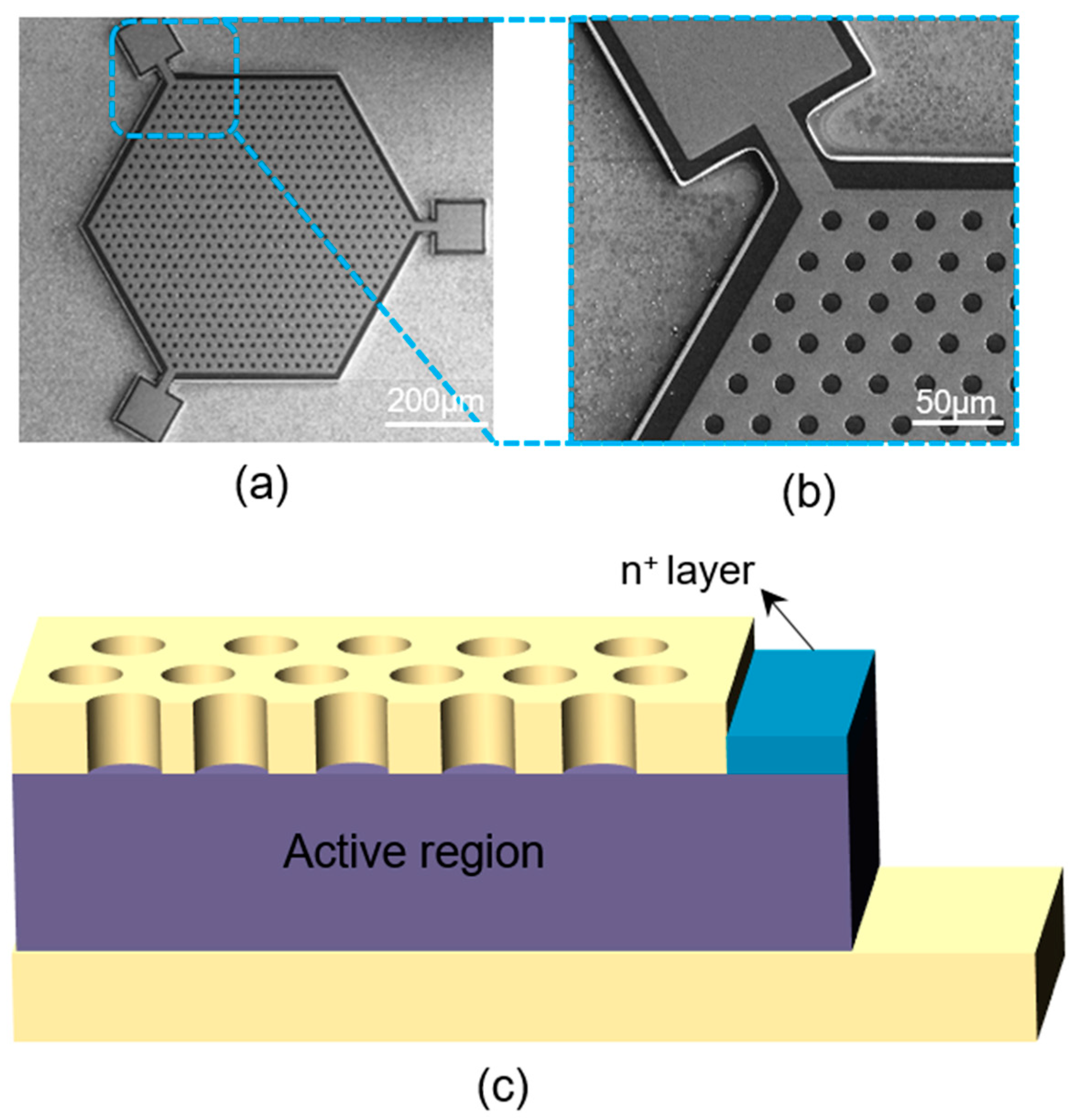
2. Materials and Methods

The THz QCL chip is based on a double-well GaAs/Al0.15Ga0.85As design with a gain bandwidth ranging from 3.0 to 3.6 THz. The thickness and quality of the active region is shown in Appendix A, Figure A1. The fabrication process of the device is based on traditional double-metal waveguide device processing [29,30], starting from In-Au thermocompression wafer bonding. Initially, the semi-insulating GaAs substrate of the original wafer was eliminated through a process involving lapping and selective wet etching. Following this, the positive-resist lithography process was employed to eliminate the 150 nm thick highly doped GaAs contact layer under the photonic crystal structure utilizing an etching solution composed of H3PO4:H2O2:H2O in a 1:1:10 concentration ratio. The circular air holes were then defined using image-reversal lithography, followed by the deposition of Ti/Au (40/300 nm) metal layers and lift-off to create the top metallic layers. To introduce the absorption boundary, the highly-doped absorption layer in the mesa periphery region with a width of 15 μm along the edge of the hexagonal mesa was retained. Then, silicon oxide with thickness of 1 μm was grown as the hard mask. Finally, hexagonal mesa structures were etched down to the bottom metal layer to minimize lateral current spreading. The scanning electron microscope (SEM) images of the PCSEL device are shown in Figure 1a,b. To realize a high symmetric far-field pattern, the hexagonal mesa device with C6 symmetry is designed and fabricated. And the photonic crystal pattern is fabricated only in the upper metal layer. Three symmetrical distributed electrodes are introduced around the hexagonal boundary of the device for current injection. This design ensures the uniform electrical injection and contributes to the highly symmetrical concentrated far field. The cross-section schematic of the PCSEL is shown in Figure 1c. The upper high-doped layer under the hexagonal mesa is removed to reduce the absorption of THz light while the high-doped layer near the mesa periphery is retained as the absorption boundary. This absorption boundary design is optimized to increase the loss of the whispering gallery modes and improve the single-mode stability of lasing [14]. Therefore, the device can work in the band edge mode introduced by photonic crystal structure steadily under large electrical pumping currents.
Devices with proper lattice constants are designed and fabricated to match with the THz QCL chip gain center so that the devices can work stably in the expected band edge mode. Figure 2a shows the calculated 2D TM band diagram of the photonic crystal structure with r / a ratio of 0.22, where r is the air hole radius. For the simulation, the effective refractive index of the active region with and without upper metal are 3.6 and 3.08, considering the active region thickness of 11.7 µ m , respectively. As shown in Figure 2a, there are many band edge modes near the central point (Γ point) of the first Brillouin zone. The electric field distribution corresponding to the band edge mode of the red curve around Γ point with a λ = 0.323 is shown in Figure 2b, which demonstrates the C6 symmetry.

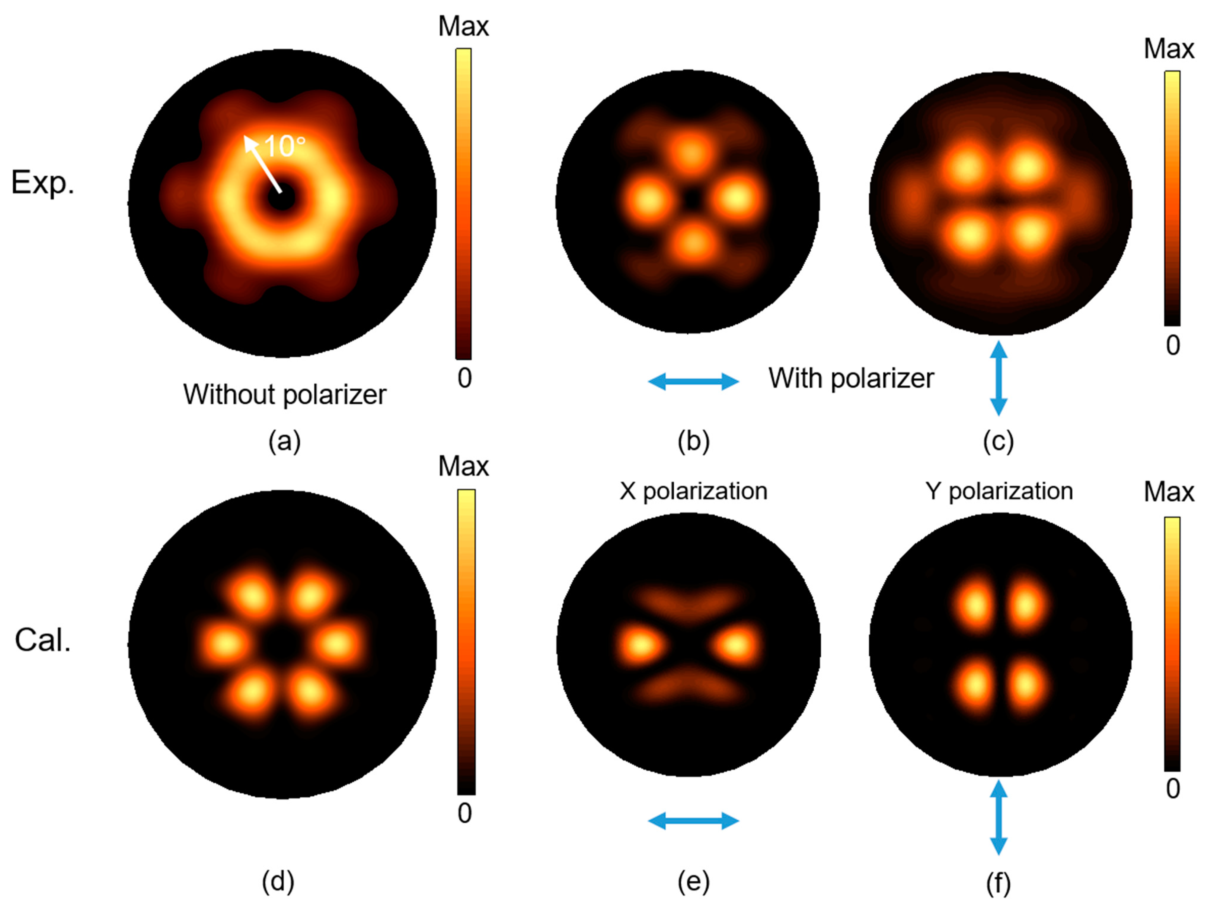
3. Results and Discussion

The measured power–current–voltage (PIV) result of the PCSEL with lattice constant a = 29   µ m is shown in Figure 3. The surface-emitting power of the device was directly measured by a Thomas Keating (TK) terahertz absolute power meter without any corrections. The device demonstrates a maximum surface emission peak power of 50 mW under a pulse condition of pulse frequency 10 KHz and duty cycle 1% at 13 K. This value is much higher than that of the THz photonic crystal lasers [13,14] reported previously. Meanwhile, the PCSEL can maintain single-mode operation over a relatively large injected current range. The relatively high single-mode stability contributes to the high-power performance, which benefits from the optimization of the absorption boundary condition and the introduction of the symmetrically distributed electrodes that ensuring the lasing in the designed band edge mode introduced by the photonic crystal structure. After the inflection point in the PIV curve, the device demonstrates multimode operation, as illustrated in the inset figure in Figure 3. Excessive injection current will result in the lasing of other band edge modes due to the increased gain of the QCL chip.
To visualize the emitting beam profile, the far-field results are measured with a high-sensitivity Golay cell detector scanning on the curve of a sphere with a radius about 15 cm. The high-frequency driven pulse is modulated into a low-frequency (20 Hz) envelope by a signal generator, and the light intensity detected by the Golay cell detector is characterized by a voltage output of a lock-in amplifier. For the far-field test, the lasers were driven near the peak power with 1 μs current pulses at a 1% duty cycle, and the test temperature was 13 K.
As shown in Figure 4a, the measured far-field pattern demonstrated a more ideal C6 symmetry compared to the reported results [13,14] with a small divergence angle of 10°, which is in good agreement with the 2D TM-wave and 3D full-wave simulated results, as is shown in Figure 2b and Figure 4d, respectively. All of the 3D full-wave and 2D TM-wave simulations were carried out based on the finite element method. The slight difference between the simulation and experimental results may originate from the noise of the detector, which leads to a decrease in the far-field contrast, thereby resulting in incomplete separation between different lobes. For further comparison, the experimental and theoretical polarized far-field patterns are obtained and displayed in Figure 4b,c and Figure 4e,f, respectively. The experimental polarized far-fields are measured by using a linear polarizer to filter the cross-polarized components which show the symmetry and distribution consistent with simulations. The good agreement of the theoretical and experimental results of the far-field indicates the lasing of the designed band edge mode of the laser.

4. Conclusions

In summary, we have reported a high-power photonic crystal surface-emitting THz laser with high beam quality. The device lased in the designed photonic crystal band edge mode, which are exemplified by the lasing spectra and far-field patterns. Through optimization of the boundary conditions and the introduction of a uniform distribution of electrodes, the far-field pattern with high symmetry and a small divergence angle is obtained, which is consistent with the simulated results. Meanwhile, the device can achieve a maximum peak surface-emitting output power of 50 mW. Our experiment realized the integration of the stable single-mode operation, high beam quality and high output power in the surface-emitting device, which is of great significance for practical applications.

Author Contributions

J.L. (Junhong Liu) conceived the idea of the research. J.L. (Junhong Liu) performed the theoretical and numerical calculations. Y.X. carried on the sample fabrications. J.L. (Junhong Liu) wrote the paper. R.L., Q.L., J.Z., S.L., S.Z., F.C., F.L. and J.L. (Junqi Liu) discussed the results. L.W. and N.Z. performed the wafer growth. Q.L. oversaw the wafer growth. J.L. (Junhong Liu) and Y.X. carried out the spectral analysis, PIV and far-field measurements. F.L. and S.Z. supervised the project. All authors have read and agreed to the published version of the manuscript.

Funding

This work is supported by the National Natural Science Foundation of China (Grant Nos. 62222408, Grant Nos. 62274014, Grant Nos. 62235016, Grant Nos.12274404), the National Key Research and Development Program of China (2021YFB3201900), and the Beijing Municipal Science & Technology Commission (Z221100002722018) in part by the Youth Innovation Promotion Association of the Chinese Academy of Sciences (2022112).

Institutional Review Board Statement

Not applicable.

Data Availability Statement

The data that support the findings of this study are available from the corresponding authors upon reasonable request.

Acknowledgments

The authors would like to thank Ping Liang and Ying Hu for their help with device processing.

Conflicts of Interest

The authors declare no conflicts of interest.

Appendix A

The thickness of one period of the active region is about 61 nm, and the total thickness of the active region for 180 periods is about 11 μm. Figure A1 shows the SEM image of the active region cross-section of the laser.
Figure A1. SEM picture of the cross-section of the active region.
Photonics 11 00150 g0a1

References

  1. Hirose, K.; Liang, Y.; Kurosaka, Y.; Watanabe, A.; Sugiyama, T.; Noda, S. Watt-class high-power, high-beam-quality photonic-crystal lasers. Nat. Photonics 2014, 8, 406–411. [Google Scholar] [CrossRef]
  2. Dikopoltsev, A.; Harder, T.H.; Lustig, E.; Egorov, O.A.; Beierlein, J.; Wolf, A.; Lumer, Y.; Emmerling, M.; Schneider, C.; Höfling, S.; et al. Topological insulator vertical-cavity laser array. Science 2021, 373, 1514–1517. [Google Scholar] [CrossRef] [PubMed]
  3. Locatelli, M.; Ravaro, M.; Bartalini, S.; Consolino, L.; Vitiello, M.S.; Cicchi, R.; Pavone, F.; De Natale, P. Real-time terahertz digital holography with a quantum cascade laser. Sci. Rep. 2015, 5, 13566. [Google Scholar] [CrossRef] [PubMed]
  4. Lei, C.; Choquette, K.D.; Zhou, D.; Seurin, J.-F.; Xu, G.; Zhao, P.; Xu, B.; Chen, T.; Van Leeuwen, R.; Matheussen, J.; et al. Progress on high-power high-brightness VCSELs and applications. In Vertical-Cavity Surface-Emitting Lasers XIX; SPIE: Bellingham, WA, USA, 2015. [Google Scholar]
  5. Grabherr, M.; Miller, M.; Jäger, R.; Michalzik, R.; Martin, U.; Unold, H.J.; Ebeling, K.J. High-power VCSEL’s: Single devices and densely packed 2-D-arrays. IEEE J. Sel. Top. Quantum Electron. 1999, 5, 495–502. [Google Scholar] [CrossRef]
  6. Jin, Y.; Gao, L.; Chen, J.; Wu, C.; Reno, J.L.; Kumar, S. High power surface emitting terahertz laser with hybrid second- and fourth-order Bragg gratings. Nat. Commun. 2018, 9, 1407. [Google Scholar] [CrossRef] [PubMed]
  7. Xu, G.; Colombelli, R.; Khanna, S.P.; Belarouci, A.; Letartre, X.; Li, L.; Linfield, E.H.; Davies, A.G.; Beere, H.E.; Ritchie, D.A. Efficient power extraction in surface-emitting semiconductor lasers using graded photonic heterostructures. Nat. Commun. 2012, 3, 952. [Google Scholar] [CrossRef] [PubMed]
  8. Zheng, C.; Qu, S.W. Loss control between symmetric and anti-symmetric modes for single-lobed surface emitting of terahertz quantum cascade laser. Opt. Express 2016, 24, 25181–25188. [Google Scholar] [CrossRef]
  9. Demichel, O.; Mahler, L.; Losco, T.; Mauro, C.; Green, R.; Xu, J.H.; Tredicucci, A.; Beltram, F.; Beere, H.E.; Ritchie, D.A.; et al. Surface plasmon photonic structures in terahertz quantum cascade lasers. Opt. Express 2006, 14, 5335–5345. [Google Scholar] [CrossRef]
  10. Kumar, S.; Williams, B.S.; Qin, Q.; Lee, A.W.M.; Hu, Q.; Reno, J.L. Surface-emitting distributed feedback terahertz quantum-cascade lasers in metal-metal waveguides. Opt. Express 2007, 15, 113–128. [Google Scholar] [CrossRef]
  11. Liang, Y.; Wang, Z.; Wolf, J.; Gini, E.; Beck, M.; Meng, B.; Faist, J.; Scalari, G. Room temperature surface emission on large-area photonic crystal quantum cascade lasers. Appl. Phys. Lett. 2019, 114, 031102. [Google Scholar] [CrossRef]
  12. Wang, Z.; Liang, Y.; Meng, B.; Sun, Y.T.; Omanakuttan, G.; Gini, E.; Beck, M.; Sergachev, I.; Lourdudoss, S.; Faist, J.; et al. Large area photonic crystal quantum cascade laser with 5 W surface-emitting power. Opt. Express 2019, 27, 22708–22716. [Google Scholar] [CrossRef] [PubMed]
  13. Chassagneux, Y.; Colombelli, R.; Maineult, W.; Barbieri, S.; Khanna, S.P.; Linfield, E.H.; Davies, A.G. Predictable surface emission patterns in terahertz photonic-crystal quantum cascade lasers. Opt. Express 2009, 17, 9491–9502. [Google Scholar] [CrossRef] [PubMed]
  14. Chassagneux, Y.; Colombelli, R.; Maineult, W.; Barbieri, S.; Beere, H.E.; Ritchie, D.A.; Khanna, S.P.; Linfield, E.H.; Davies, A.G. Electrically pumped photonic-crystal terahertz lasers controlled by boundary conditions. Nature 2009, 457, 174–178. [Google Scholar] [CrossRef] [PubMed]
  15. Yoshida, M.; De Zoysa, M.; Ishizaki, K.; Tanaka, Y.; Kawasaki, M.; Hatsuda, R.; Song, B.; Gelleta, J.; Noda, S. Double-lattice photonic-crystal resonators enabling high-brightness semiconductor lasers with symmetric narrow-divergence beams. Nat. Mater. 2018, 18, 121–128. [Google Scholar] [CrossRef] [PubMed]
  16. Yoshida, M.; Katsuno, S.; Inoue, T.; Gelleta, J.; Izumi, K.; De Zoysa, M.; Ishizaki, K.; Noda, S. High-brightness scalable continuous-wave single-mode photonic-crystal laser. Nature 2023, 618, 727–732. [Google Scholar] [CrossRef] [PubMed]
  17. Vitiello, M.S.; Nobile, M.; Ronzani, A.; Tredicucci, A.; Castellano, F.; Talora, V.; Li, L.; Linfield, E.H.; Davies, A.G. Photonic quasi-crystal terahertz lasers. Nat. Commun. 2014, 5, 5884. [Google Scholar] [CrossRef] [PubMed]
  18. Biasco, S.; Ciavatti, A.; Li, L.; Giles Davies, A.; Linfield, E.H.; Beere, H.; Ritchie, D.; Vitiello, M.S. Highly efficient surface-emitting semiconductor lasers exploiting quasi-crystalline distributed feedback photonic patterns. Light Sci. Appl. 2020, 9, 54. [Google Scholar] [CrossRef]
  19. Xie, Y.-Y.; Ni, P.-N.; Wang, Q.-H.; Kan, Q.; Briere, G.; Chen, P.-P.; Zhao, Z.-Z.; Delga, A.; Ren, H.-R.; Chen, H.-D.; et al. Metasurface-integrated vertical cavity surface-emitting lasers for programmable directional lasing emissions. Nat. Nanotechnol. 2020, 15, 125–130. [Google Scholar] [CrossRef]
  20. Meng, Y.; Chen, Y.; Lu, L.; Ding, Y.; Cusano, A.; Fan, J.A.; Hu, Q.; Wang, K.; Xie, Z.; Liu, Z.; et al. Optical meta-waveguides for integrated photonics and beyond. Light Sci. Appl. 2021, 10, 235. [Google Scholar] [CrossRef]
  21. Faist, J.; Capasso, F.; Sivco, D.L.; Sirtori, C.; Hutchinson, A.L.; Cho, A.Y. Quantum cascade laser. Science 1994, 264, 553–556. [Google Scholar] [CrossRef]
  22. Vitiello, M.S.; Scalari, G.; Williams, B.; De Natale, P. Quantum cascade lasers: 20 years of challenges. Opt. Express 2015, 23, 5167–5182. [Google Scholar] [CrossRef] [PubMed]
  23. Yao, Y.; Hoffman, A.J.; Gmachl, C.F. Mid-infrared quantum cascade lasers. Nat. Photonics 2012, 6, 432–439. [Google Scholar] [CrossRef]
  24. Köhler, R.; Tredicucci, A.; Beltram, F.; Beere, H.E.; Linfield, E.H.; Davies, A.G.; Ritchie, D.A.; Iotti, R.C.; Rossi, F. Terahertz semiconductor-heterostructure laser. Nature 2002, 417, 156–159. [Google Scholar] [CrossRef] [PubMed]
  25. Wang, Z.; Liang, Y.; Yin, X.; Peng, C.; Hu, W.; Faist, J. Analytical coupled-wave model for photonic crystal surface-emitting quantum cascade lasers. Opt. Express 2017, 25, 11997–12007. [Google Scholar] [CrossRef]
  26. Kogelnik, H.; Shank, C.V. Coupled-Wave Theory of Distributed Feedback Lasers. J. Appl. Phys. 1972, 43, 2327–2335. [Google Scholar] [CrossRef]
  27. Contractor, R.; Noh, W.; Redjem, W.; Qarony, W.; Martin, E.; Dhuey, S.; Schwartzberg, A.; Kante, B. Scalable single-mode surface-emitting laser via open-Dirac singularities. Nature 2022, 608, 692–698. [Google Scholar] [CrossRef] [PubMed]
  28. Yao, D.-Y.; Zhang, J.-C.; Cathabard, O.; Zhai, S.-Q.; Liu, Y.-H.; Jia, Z.-W.; Liu, F.-Q.; Wang, Z.-G. 10-W pulsed operation of substrate emitting photonic-crystal quantum cascade laser with very small divergence. Nanoscale Res. Lett. 2015, 10, 177. [Google Scholar] [CrossRef]
  29. Unterrainer, K.; Colombelli, R.; Gmachl, C.; Capasso, F.; Hwang, H.Y.; Sergent, A.M.; Sivco, D.L.; Cho, A.Y. Quantum cascade lasers with double metal-semiconductor waveguide resonators. Appl. Phys. Lett. 2002, 80, 3060–3062. [Google Scholar] [CrossRef]
  30. Khalatpour, A.; Paulsen, A.K.; Deimert, C.; Wasilewski, Z.R.; Hu, Q. High-power portable terahertz laser systems. Nat. Photonics 2020, 15, 16–20. [Google Scholar] [CrossRef]
Figure 1. (a,b) Scanning electron microscope (SEM) images of the terahertz photonic crystal laser. The size of the three charged electrodes is 100 × 100 µ m 2. The absorption boundary width is 15 µ m . (c) The cross-section schematic of the PCSEL. The top n+ layer under the hexagonal mesa region is removed while that in the mesa periphery area is retained as the absorption boundary.
Photonics 11 00150 g001
Figure 2. (a) The calculated 2D transverse magnetic photonic crystal band diagram with r / a ratio of 0.22. Different color lines represent different energy bands. Inset: the first Brillouin region and the high symmetry point corresponding to the photonic crystal band. (b) The out-of-plane electric field distribution (Ez) of the low band edge mode with C6 symmetry.
Photonics 11 00150 g002
Figure 3. PIV curve of devices with a = 29   µ m under 13 K with a pulse condition of 1% (10 KHz, 1 μs) The black and red lines correspond to voltage and power, respectively. Inset: lasing spectrum of the device under different injection currents. The colors of the lasing spectrums and the labeled points in the power curves correspond to each other.
Photonics 11 00150 g003
Figure 4. (a) The experimental far-field pattern. (b,c) The experimental polarized far-field pattern. For the experimental result, the device was measured at 13 K with a pulse condition of 1% (10 KHz, 1 μs). The blue arrow represents the linear polarization direction. (d) The calculated far-field pattern. (e,f) The calculated polarized far-field patterns considering the same polarization as the experiment.
Photonics 11 00150 g004
Disclaimer/Publisher’s Note: The statements, opinions and data contained in all publications are solely those of the individual author(s) and contributor(s) and not of MDPI and/or the editor(s). MDPI and/or the editor(s) disclaim responsibility for any injury to people or property resulting from any ideas, methods, instructions or products referred to in the content.

