1. Introduction
Non-destructive optical techniques are crucial in almost all disciplines of science, especially in the field of materials science, like the thin-film characterization in photovoltaics, microelectronics, and other tasks, as they can be used during all stages of the manufacturing process of material samples. One such technique is spectroscopic ellipsometry (SE). SE is a non-destructive, non-invasive, and non-intrusive optical technique. It measures the relative change in the polarization state of the measurement beam induced by reflection from or transmission through a sample. Generally, the ellipsometry technique uses collimated light beams with a well-defined angle of incidence to illuminate the sample. Nevertheless, a non-parallel expanded light beam with precision suitable for real-time mapping, production lines, and quality control can also be used [
1].
During in situ real-time measurement, fabrication, and processing, ellipsometry is used to analyze the multilayered film structures, interfaces, and composites, and it is famous for its extreme sensitivity to very thin over layers well below 1 nm thickness [
2], which, together with its high-speed measurement capability, makes it an efficient optical mapping tool for thin-film solar cells. Under appropriate circumstances, SE determines film thicknesses more accurately than any other known technique [
3].
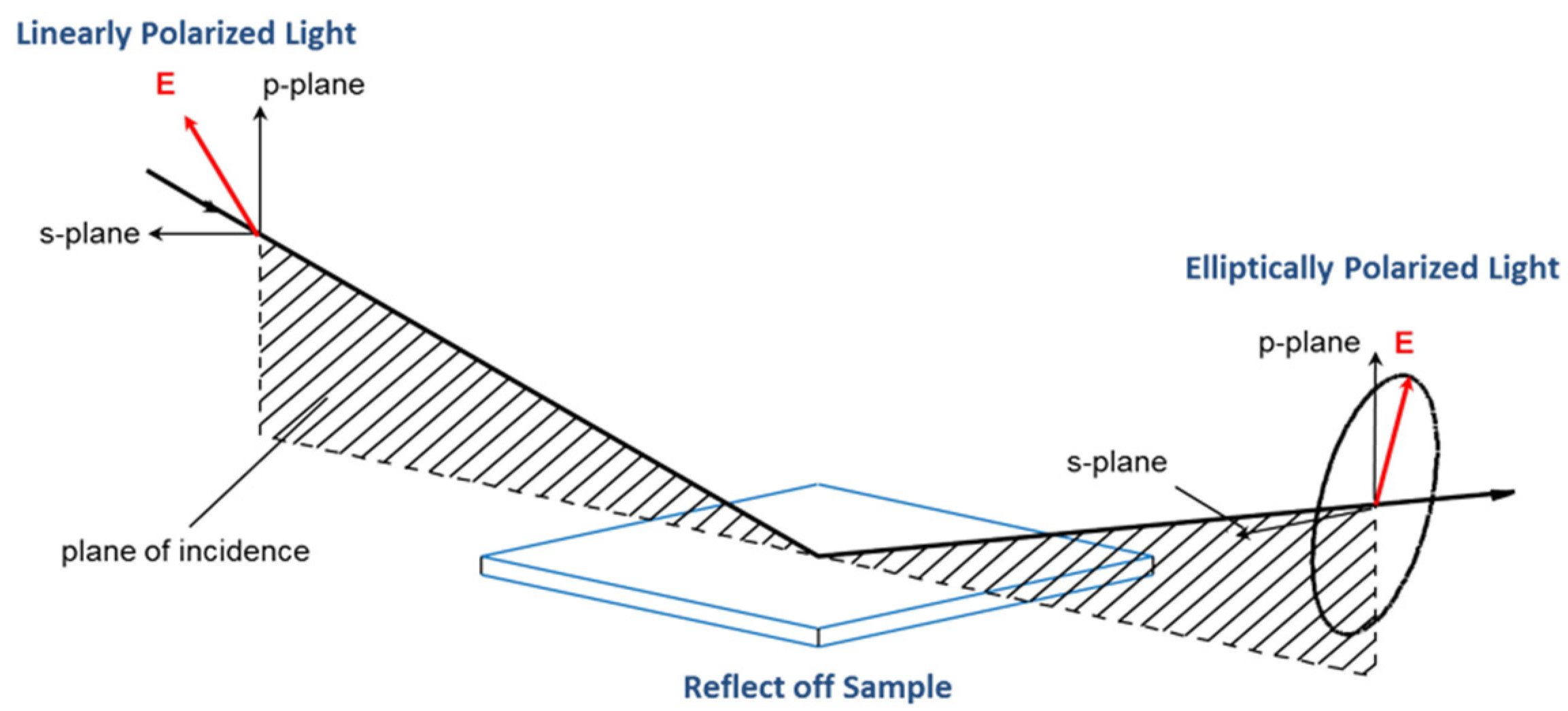
Ellipsometry measures the amplitude ratio tan ψ and phase difference Δ between the p- and s-polarizations [
4], which depends on the wavelength of the light beam (λ) and the angle of incidence of the beam (θ) at the sample surface; see
Figure 1.
It should be noted that this technique cannot be used at a normal angle of incidence, as the s-polarizations (perpendicular to the plane of incidence) and the p-polarizations (parallel to the plane incidence) cannot be distinguished from one another, which makes the choice of the incidence angle more important. For semiconductors, the angle of incidence is typically between 60° and 80°. Generally, in ellipsometry, the angle of incidence is set at the Brewster angle [
5]. The general working principle of spectroscopic ellipsometry is depicted in
Figure 1.
In the case of light reflection, the measured complex reflectance ratio ρ is equal to
where tan
ψ is the amplitude ratio, Δ is the phase difference,
rp = reflection coefficient for p-polarized light, and
rs = reflection coefficient for s-polarized light.
During data analysis, information about the sample under study is obtained by fitting measured ellipsometry spectra to optical and structural models, as ellipsometry does not give direct information about the sample in consideration.
The purpose of this work is to make a well-calibrated prototype optical mapping tool for thin-film measurements using only cheap parts, such as an LCD monitor and a pinhole camera with CMOS Sensor (The Imaging Source Europe GmbH, Bremen, Germany) with an Integrated 4-Directional Wire Grid Polarizer Array (Sony’s IMX250MYR CMOS (Macnica ATD Europe Inc., Chatou, France)). Sony’s Pregius line of CMOS image sensors.
During conventional ellipsometric mapping, data collection is relatively slow and uses a small scanned spot, while our new optical mapping tool made from cheap parts measures a big area in one shot. Specifically, in this paper, the special focus is on a newly developed calibration method. The thickness map result is independently cross-checked using a commercial Woollam M2000 ellipsometer (J.A. Woollam Co. Inc., Lincoln, NE, USA), and the agreement is within 1 nm, which makes our optical mapping tool a good candidate for industrial purposes.
We know two industrial systems which are capable of measuring big (square-meter size) samples: the Semilab FPT system (
https://semilab.com/hu/product/799/fpt (Accessed on 30 September 2024)) and the Woollam AccuMap (
https://www.jawoollam.com/download/pdfs/accumap-se-brochure.pdf (Accessed on 30 September 2024)) system. Both systems use a “traditional” SE device (100 kUSD price) in special big moving/scanning systems, measuring the big samples point by point. The Woollam brochure states that “Data Acquisition Rate: <6 s per point (includes time for movement to new point, automated alignment, and data collection)” so it can measure one big area during several 10 min time periods. Our system can measure within seconds during one shot.
2. Materials and Methods
SiO2 on Si samples with a nominal thickness of 40, 60, and 100 nm, 20 cm in diameter, were used for the calibration of the angle of incidence and ρ-correction, and another SiO2/Si sample with a nominal thickness of 80 nm was used as an independent check.
Note that silicon dioxide is one of the most studied materials and is widely used in the semiconductor industry due to its huge abundance, affordability, and technological importance. The homogeneity of the SiO
2 film was proved to be a maximum of 5 nm across the samples, qualifying it as a patterned large-area reference sample for film thickness [
6].
Our optical mapping tool consists of a polarization-sensitive camera (The Imaging Source Company’s DYK 33UX250 USB 3.0 Polarsens camera, a 2/3 inch Sony CMOS Pregius Polarsens sensor of model IMX250MZR Integrated with 4-Directional Wire Grid Polarizer Array) with a pinhole of sub-mm size in front of it, a sample holder, and an LCD monitor (Dell UltraSharp™ U2412M, GB-LED (Dell Magyarország Kft. Budapest, Hungary)) as a light source for the illumination of the selected sample. See
Figure 2 below for the schematics of the experimental setup diagram.
Notice that our optical mapping ellipsometer uses a non-collimated beam (coming from the monitor screen) as a source of light, despite most conventional ellipsometers using collimated light beams with a well-defined angle of incidence. Our arrangement shows a similarity to the solution of Bakker et al. [
7], who used a computer screen as a light source and a webcam as a detector in an imaging off-null ellipsometer. The basis of this work is a patent from our Institute: Horváth Z Gy, Juhász G, Fried M, Major C, Petrik P: Imaging optical inspection device with a pinhole camera; EP2160591B1, submission number: PCT/HU2008/000058, NSZO: G01N21/8422, country of patent: Europe.
The non-collimated beam ellipsometer setup is shown in
Figure 2. An LED-LCD monitor serves as a polarized RGB-colored light (see the built-in polarizer sheet, number 4 in
Figure 2) and a polarization-sensitive camera behind a pinhole (7&8) together. The LCD monitor (Dell UltraSharp™ U2412M, GB-LED) is used in a 45-degree rotated position, measured by a digital angle gauge with 0.1 deg precision. In a straight-through position, we can detect the extinction of the polarization-sensitive camera better than 10
−2.
The polarization-sensitive camera sensor (The Imaging Source Company’s DYK 33UX250 USB 3.0 Polarsens camera) provides the polarization state data from 0-, 45-, 90-, and 135-degree rotation positions (plus 3 RGB colors in each position). This arrangement is similar to a conventional static photometric rotating analyzer ellipsometer.
The sample is illuminated by a non-collimated light through a fixed polarizer at an azimuth of 45 degrees to the plane of incidence. The reflected light passes through a virtual “rotating analyzer” and the intensity is captured by a two-dimensional position-sensitive photodetector system at four different angular positions of the analyzer.
A minimum of 3 different analyzer positions are required. These four polarization states’ (intensity) data (at 0-, 45-, 90-, and 135-degrees rotation positions) are enough (the fourth source of data is good for reducing the error) to determine the ellipsometric angles: ψ and Δ. Our camera provides data for 3 colors, so we measured ψ and Δ as 3 × 2.
Three SiO2 samples with different thicknesses (nominally 40 nm, 60 nm, and 100 nm) on silicon substrates were used for the calibration process.
The monitor correction is calculated using the following equation:
where
ρopt is the measured value with a perfect light source,
ρmeas is the actually measured value, and
ρmonitor is the ρ-correction. We measure three SiO
2/Si samples with different thicknesses. We determine 3*N*2 ψ and Δ (where N is the number of different wavelengths, presently 3), and we should calculate (fit) 2*N + 3 + 1 unknown calibration values for a full calibration: N*real (ρ
monitor) and N*im(ρ
monitor) + 3 thicknesses + 1 actual angle of incidence in each point and each wavelength. Each thickness and angle of incidence in the sample depends only on the location, but the ρ-corrections (ρ
monitor) are location- and wavelength-dependent. This implies that ρ-corrections give more insight into the nature and status of the sample measurement.
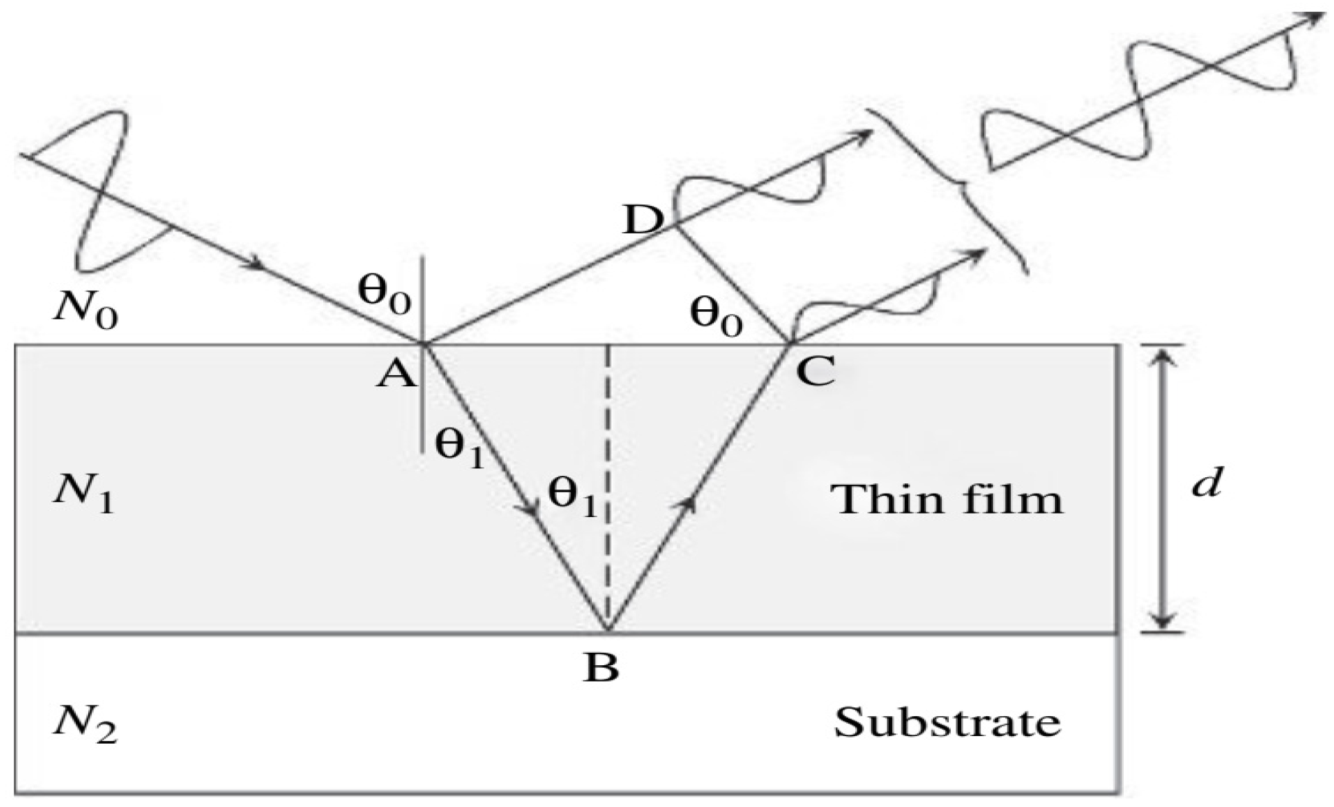
Note that the basic equations for these evaluations are the Fresnel equations. Below are the schematic diagram, shown in
Figure 3, and the equations for the optical interference in an ambient/thin-film/substrate optical model, Equations (1) and (2).
where
N = n − ik is the complex refractive index. Here, n is the refractive index, k is the extinction coefficient, and i is the imaginary unit.
r and t are the complex reflection coefficient and complex transmission coefficient for p- (parallel) and s-polarized (normal) lights, respectively.
The j (0 or 1) and k (1 or 2) subscripts represent corresponding parameter values in the case of air (0), thin-film (1), or substrate (2) reflection or transmission of the light. Jk = “01” in the case of an air/thin-film interface and “12” in the case of a thin-film/substrate interface.
θj and
θk are the angle of incidence and transmission, respectively, and are related by Snell’s law:
Ellipsometry is an indirect measurement method; generally, the measured values (ellipsometric angles) cannot be converted directly into physical parameters, i.e., thicknesses and optical constants of the sample. Normally, an optical model is supposed and a fitting procedure is used to evaluate the variable parameters. Finding the best match between the model and the experiment is typically achieved through regression, where the computer program calculates the ellipsometric angles (based on the optical model) and compares them with the measured ones. An estimator, such as the mean square error (MSE), is used to quantify the difference between the calculated and measured ellipsometric angles. A lower MSE indicates a better fit and better optical model. In our calibration process, we fit the angle of incidence (wavelength-independent), the 3 thicknesses (wavelength-independent), and the ρmonitor (location- and wavelength-dependent) point by point for each pixel throughout the sample.
A special software or program is required to perform this complicated calibration process, because we should fit the results in a complicated manner, fitting all 10 unknown parameters at the same time using the measurements of the 3 different oxides. Mainly, a MatLab program (version matlab2015a) with some other complementary software was used in our case to analyze and interpret the experimental results.
Each 20 cm diameter oxide sample was placed at six different positions on the 30 × 30 cm holder; see
Figure 4. From the device geometry (
Figure 2), we can calculate a 50–80-degree region for the possible angle-of-incidence region, but practically, a 60–80-degree region is usable.
After the fitting procedure, we obtained the thickness values, the angle-of-incidence values, the ρmonitor values, and the MSE (mean square error, the goodness of the fit), which is the squared difference between the measured and calculated ψ and Δ values. The fitted thickness, the angle, and the ρ values were collected according to the low MSE values. As each oxide sample was put at a specific position on the substrate, significant errors could be seen in several places due to the edges or the insufficient illumination from the monitor. We merged the maps according to the lower MSE and checked which parts of the maps (angle of incidence, thicknesses, and ρmonitor values) are “smooth” enough. As a result, the pixels in the mapping figures were truncated where the MSE was not low enough and where values changed in a step-like manner. At last, we determined that we can reliably use only the central 20 × 15 cm part.
3. Results
It is a common scientific practice to check any device or setup for accuracy and precision and to try to correct any errors or malfunctions in the setup through calibration and comparison with other corresponding standard models. Accordingly, a direct monitor measurement was taken in our setup, and we noticed, or rather, confirmed that we needed error correction and calibration of the experiment setup.
Theoretically, perfect linearly polarized light was coming from the monitor at three different (red, green, and blue) light-bands. We directed the camera to the monitor to perform a direct ellipsometric measurement without a sample; see
Figure 5. If we have an ideal sample, which does not change the polarization state, then we measure tan ψ and cos Δ values to 1 in each point. This measurement shows the fact that a point-by-point ρ-correction calibration is needed.
Figure 6 shows the result of direct monitor measurements and the tan ψ and cos Δ values for each color, red, blue, and green. The systematic alterations from 1 in the maps show systematic measurement errors in our optical mapping tool that justify the need for special calibration.
Three SiO
2/Si samples with a nominal thickness of 40, 60, and 100 nm were used for the calibration process, and another SiO
2/Si sample with a nominal thickness of 80 nm was analyzed using the calibration values from the three oxide samples. The experimental data were collected for each of the three oxide samples, and then, six different positions of each sample were used in the calibration process. The experimental figures shown in this paper are mostly deduced by excluding pixels with high MSE values that deviate the results from the true expected values, prioritizing points of only low MSE.
Figure 7b shows the MSE map of the central 20 × 15 cm part where the measurement proved to be reliable.
The result of the angle-of-incidence calibration is shown in
Figure 8. Using the same criteria (low MSE, smooth map), we refined the angle-of-incidence map (
Figure 8b) from the full angle-of-incidence map (
Figure 8a). As seen in
Figure 8b, the angle of incidence varies smoothly across the surface, which agrees with the theoretical values. This refined angle-of-incidence map was used later to evaluate the thickness map of the SiO
2/Si sample with a nominal thickness of 80 nm.
The same calibration process resulted in the thickness maps of our calibration oxide samples (nominal thickness of 40, 60, and 100 nm), which are shown below in
Figure 9.
The calibrated ρ
monitor values for the specific settings of the device are also mapped; see
Figure 10. These values differ from the ideal values only by less than 0.3, so we can use them to evaluate independent measurements.
We used a SiO
2/Si sample with a 20 cm diameter and a 80 nm nominal thickness to check the results of the calibration. We used the calibrated ρ
monitor values to correct the measured ellipsometric angles and used the corrected values to determine the thickness map. The thickness map of the 80 nm oxide sample in
Figure 11b appears to be smooth enough. Note that one color in
Figure 11 is only 0.5 nm.
An independent checking measurement of the same sample was also made by the Wollam M2000 ellipsometer, as shown in
Figure 11a. The agreement between the thickness measurement made between our non-collimated ellipsometer after correction and the conventional Wollam M2000 ellipsometer is only within 1 nm, which is a good agreement.

 ,
, 