1. Introduction
Microwave phased arrays have been widely used in conventional radar systems. Due to the rapid development of laser detection and ranging (LADAR) and free-space optical communication (FSO), the optical phased array (OPA) is the most significant component of solid-state systems [
1]. Silicon photonic platforms, which are CMOS compatible, low-cost and energy-efficient, enable the integration of OPA on one chip.
In the OPA chip, the antenna and laser source are the key components. The optical antenna, with the large separation to avoid crosstalk, will cause high-order grating lobes in the far-field [
2,
3]. The method of sparse aperiodic array arrangement can be used to suppress the far-field side-lobe of a large array spacing arrangement, and the simulation results show that a very small side mode rejection ratio can be obtained within the scanning angle of 180° [
4]. However, the far-field energy of this scheme cannot be concentrated on the main lobe. If the half-wavelength interval method is adopted, the problem of grating lobes can be solved and the optical power can be more concentrated on the main lobe. Arrays with non-uniform waveguide spacing [
5,
6] and apodized amplitude [
7] have been proposed to compress the grating lobes, but the suppression ratios are still low. The one-dimensional silicon-based optical phased array with an interval of 775 nm was demonstrated. The beam steering angle of 60° in one dimension was measured [
8]. Using a half-wavelength interval waveguide to realize one-dimensional scanning has also been proposed in our previous work, and the scanning angle was measured to be 40° [
9]. The curved waveguide array is also utilized to reduce the crosstalk of one-dimensional array elements [
10,
11]. However, these grating lobe-free OPAs based on the silicon-on-insulator (SOI) platform are found to have a lack of integrated lasers. The III–V platform has the capability of realizing the monolithically heterogeneous integration of the laser and modulators [
12,
13,
14]. However, the integration process has a high requirement of state-of-the-art process and has a high cost.
In this paper, a 1 × 16 one-dimensional OPA chip hybrid integrated with a III–V laser is proposed and demonstrated. The III–V distributed feedback (DFB) laser chip is vertically coupled with a silicon OPA chip based on a chirped grating coupler of a large bandwidth. The coupling efficiency can also be increased by utilizing the metal reflector underneath the silicon oxide layer. To overcome the limitation of grating lobes, the waveguide array of a half-wavelength interval and a non-uniform width is utilized as the antenna array. Based on this design, the beam steering system based on OPA can have a wide field of view and a compact size.
2. Design and Analysis
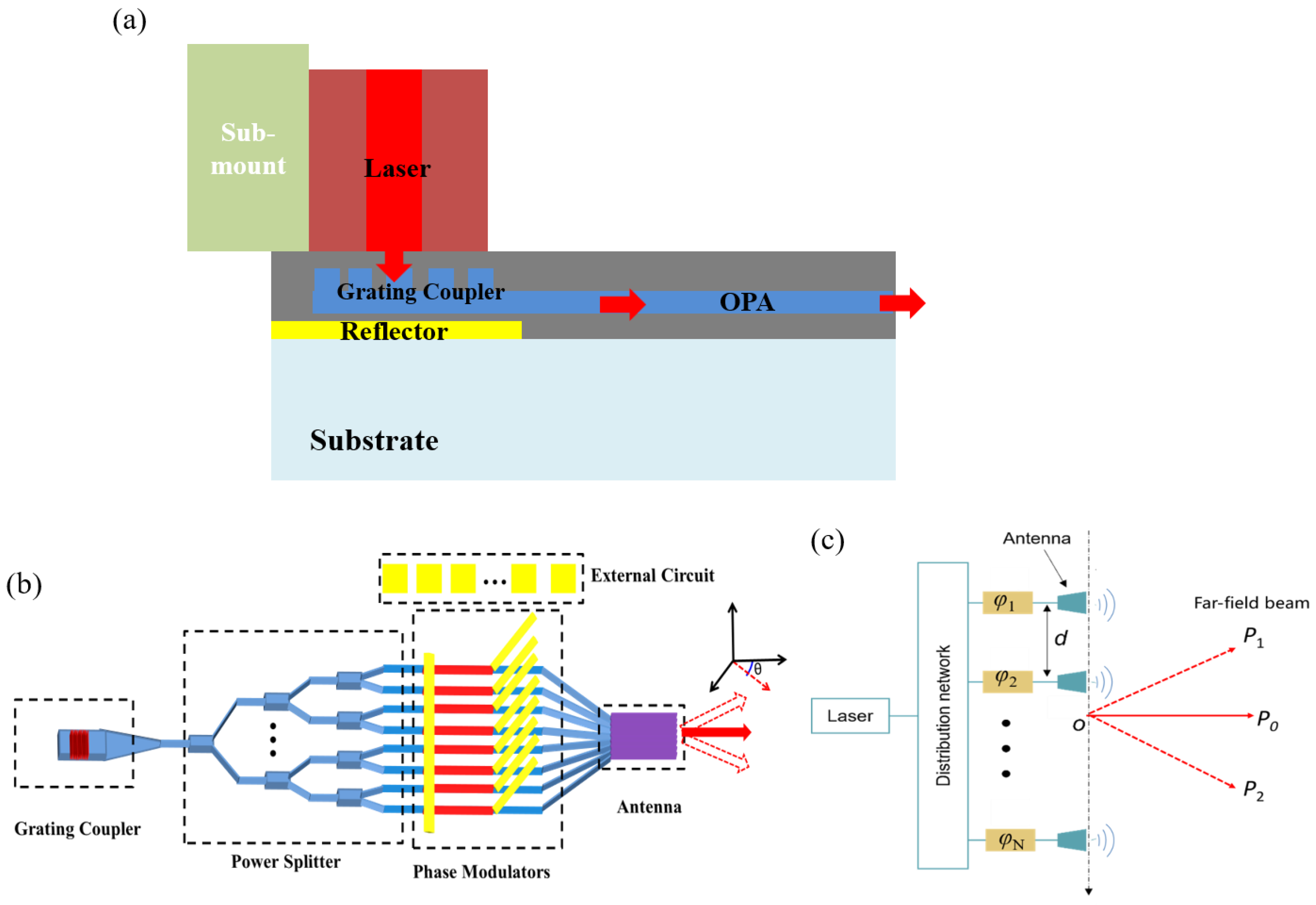
The schematic diagram of the proposed integrated chip for beam steering is shown in
Figure 1a. The III–V DFB laser is hybrid integrated with the OPA chip. The grating lobe-free 1 × 16 integrated OPA is shown in
Figure 1b. The OPA chip consists of grating coupler, optical beam splitters, a phase modulator array and optical antennas. The power of the laser source is uniformly distributed to the phase modulators via the beam splitter tree. The optical wavefront is controlled using the phase modulator array. The far-field intensity distribution of an optical phased array can be calculated using the principle of multi-beam interference superposition, as shown in
Figure 1c. The SOI platform with a 220 nm-thick silicon layer is considered for OPA chip in this work. The proposed OPA operates at a 1550 nm wavelength and TE polarization.
Conventionally, the optical modes of III–V waveguide and silicon waveguide are integrated with large mode mismatch. It is difficult to realize a low insertion loss. Here, the chirped grating coupler is utilized to couple the broadband light vertically from the III–V laser to the silicon OPA chip, as shown in
Figure 2a. The height of the silicon waveguide
h is 220 nm and the etch depth
he of the grating is 70 nm. Due to the high computational cost of optimizing a full three-dimensional (3D) grating coupler, a two-dimensional (2D) finite difference time domain (FDTD) method combined with an inverse design method is used for parameter optimization, as shown in our previous work [
15]. The inverse design method based on a gradient will not rely on parameter scanning or random perturbation and will save simulation time compared with the genetic algorithm or particle swarm optimization. The figure of merit (FOM) is defined as follows:
where
CEλn is the coupling efficiency of the
n-th wavelength
λn. The coupling efficiency is the transmission of the laser mode coupled to the single mode of the silicon waveguide. The FOM is the maximum of the average coupling efficiencies over a wavelength range. The grating coupler is optimized at the center wavelength of 1550 nm and with the 3 dB bandwidth of 100 nm as optimal target values. The calculated insertion loss is larger than 4 dB without the reflector, as shown in
Figure 2b. To further improve the coupling efficiency, a metal reflector is set underneath the chirped grating coupler, of which the spacing
t is 900 nm. The optimized results are verified by using the 3D-FDTD method, and the parameters of the grating coupler are shown in
Table 1. The coupling efficiency can be up to 0.45 dB (90%) and the 3 dB bandwidth is about 90 nm with the metal reflector underneath the silicon oxide layer, which has a higher performance than the conventional grating coupler.
The input power is equally divided into 16 channel phase shifters by utilizing cascaded 3 dB couplers, which is based on a multimode interference (MMI) coupler. Then, the light is modulated by 16 independent phase shifters, which are realized via the thermo-optic effect of silicon. Finally, the light with a specific phase is emitted from the butt-coupled waveguide array. The optical antennas with small spacing (
d) are utilized to suppress these high-order (
m) grating lobes [
9]. The grating lobe angle (
θm) is defined according to the following formula:
where
λ is the optical wavelength and Δ
φ is the phase difference between antennas. When the spacing satisfies
d ≤
λ/2, non-grating lobes will exist. Thus, the spacing of the waveguide is chosen to be 750 nm and is smaller than half of the wavelength 1550 nm. Furthermore, the beam steering angle can be up to ±90°, with a phase difference in ±π between phase shifters. Considering the phase mismatch condition to suppress the crosstalk of the antennas [
16], the widths of the adjacent waveguide pair are chosen to be 450 nm, 550 nm, 400 nm and 600 nm as an example. The optical crosstalk is below −30 dB among 20 μm-long waveguide arrays.
The far-field beam angle is controlled using the phase modulator array of OPA. The phase shifter is based on the thermo-optic effect of silicon material. The thermo-optic coefficient is about 1.86 × 10
−4/K. We use the HEAT Solver in DEVICE Solutions to simulate the thermal field distribution of the heater. To calculate the change in the effective refractive index, the thermal field distribution is imported to MODE Solutions. The relationship between the phase difference Δ
φ and beam steering angle
θ is deduced to the following equation:
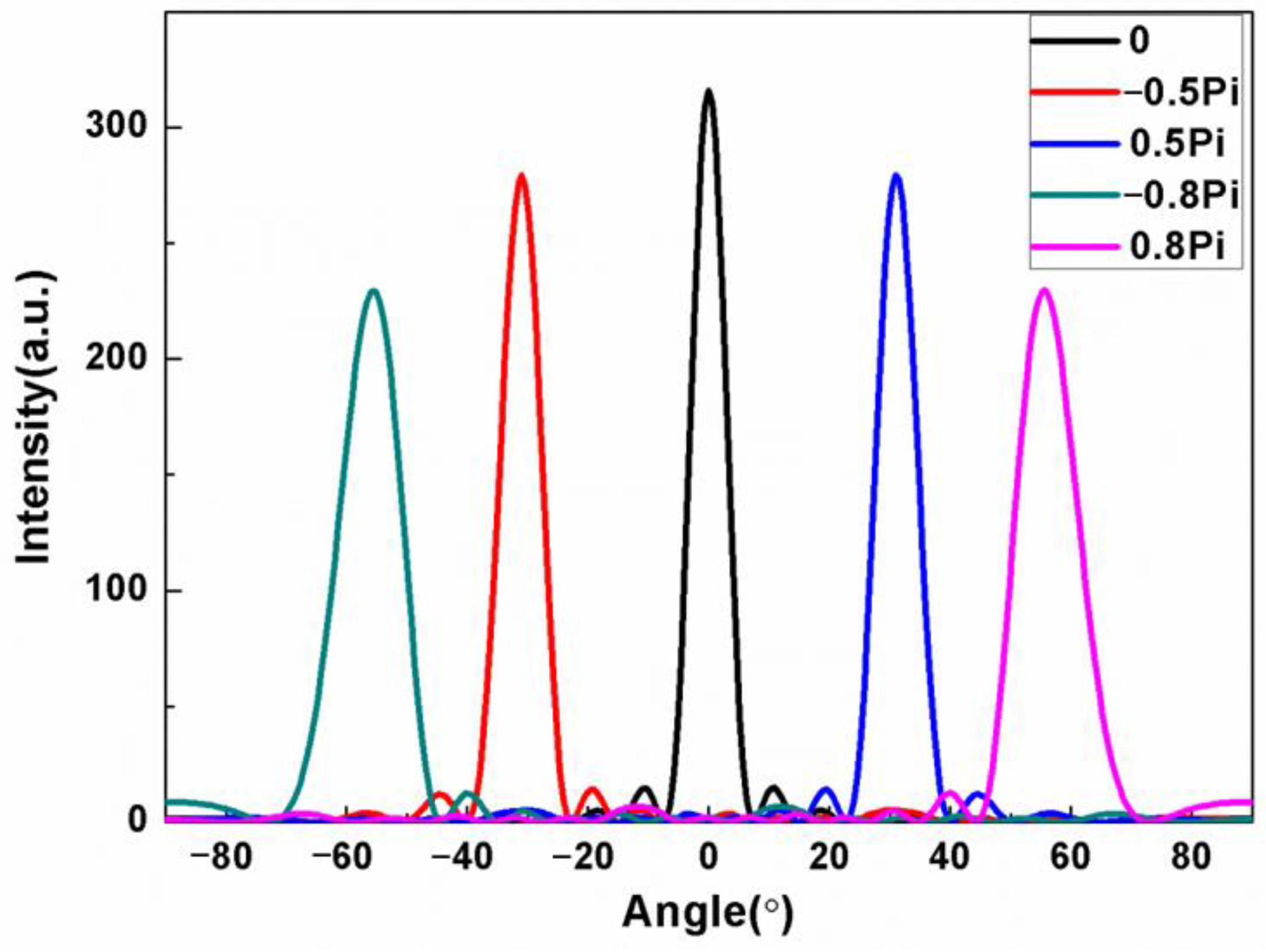
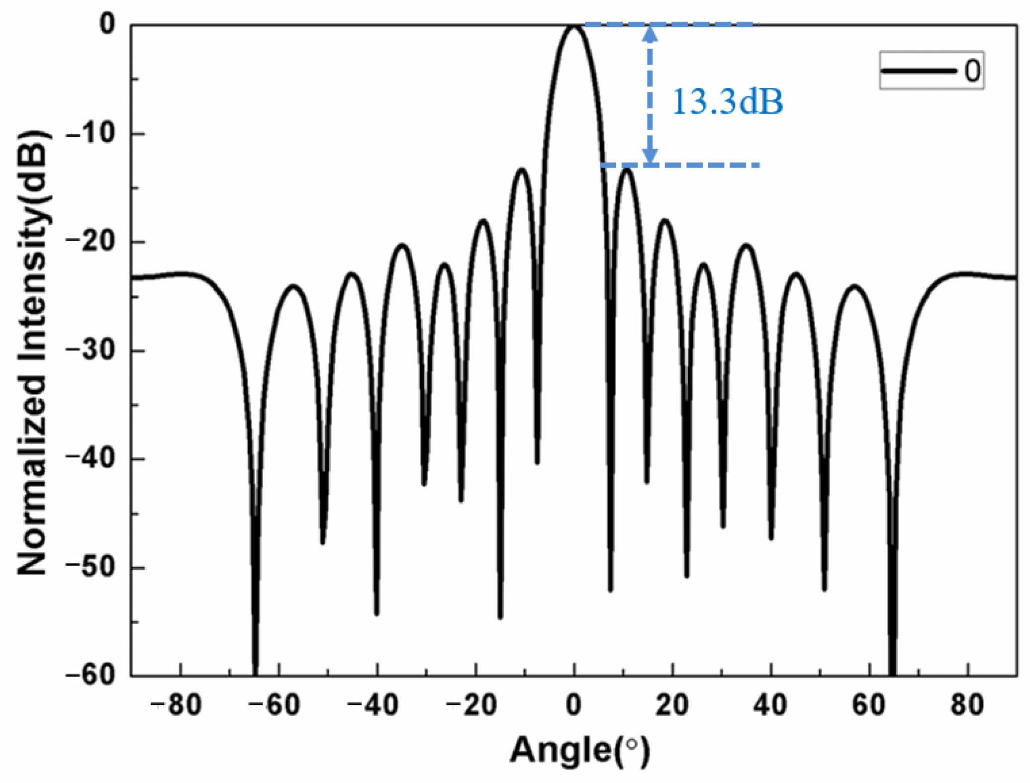
Figure 3 shows the calculated optical far-field distribution of the proposed OPA with half-wavelength spacing. The special design can fully eliminate the high-order grating lobes in a 180°-wide field of view (FOV). As shown in
Figure 4, there is no grating lobe in the FOV and the side-lobe suppression ratio is about 13.3 dB.
3. Results and Discussion
The OPA chip is fabricated on the SOI platform with a top silicon layer of 220 nm thickness and a buried oxide layer of 2 μm thickness. The main fabrication flow is shown in
Figure 5. Firstly, the electron beam lithography (Raith150 II) is used to define the patterns on the photoresist layer. The device patterns are then transferred onto the silicon layer using inductively coupled plasma reactive-ion etching (ICP-RIE) with a gas mixture. The silica top cladding layer is 900 nm thick, which is consistent with the high coupling efficiency of the grating coupler, and is deposited via plasma-enhanced chemical vapor deposition (PECVD). The gold/titanium of 5 nm/100 nm thickness that are utilized as thermal heaters, and the gold utilized as pads for wire bonding, are developed using electron beam evaporation. Then, the SOI chip is flip bonded with the quartz substrate and the upper silicon substrate is removed and polished with the chemical mechanical polishing (CMP) method. Finally, the lithography and ICP are used to etch the silicon oxide, which can open the windows above these metal pads.
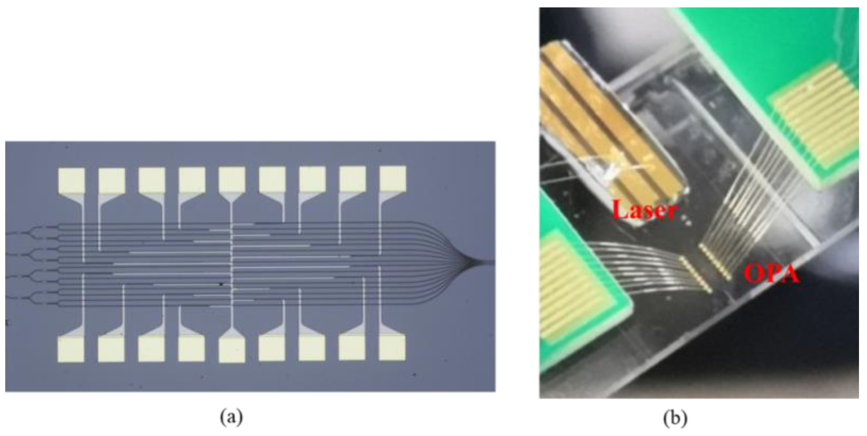
Figure 6a shows the optical microscope image of the fabricated 16-channel OPA. The phase shifters are based on thermo-optic effect. The metal pads are wire-bonded to the external printed circuit board (PCB) connected to the multi-channel voltage controller. The commercial III–V DFB laser chip coupled and packaged with the silicon OPA chip, as shown in
Figure 6b.
We also characterize the key components of the OPA chip. To characterize the coupling efficiency of the chirped grating coupler, the III–V DFB laser at a 1550 nm wavelength and with an output power of 4 dBm is utilized as the source. The photodetector connected with the single mode fiber is used to read out the transmissions. The normalized coupling efficiency of the chirped grating coupler is about 3.3 dB at a 1550 nm wavelength, which is mainly dependent on the thickness of the silicon oxide layer and the etching depth/width of the grating. The insertion loss of the OPA chip is about 5.3 dB. To characterize the phase modulation effect of the thermo-optic modulator, a Mach–Zehnder interferometer with one arm modulated using the electronic heater is fabricated on the same chip. For the π phase shift, the measured electric power is about 1.6 mW under a voltage of 1.8 V, which is compatible with most transistor–transistor logic circuits. The low power consumption is mainly due to the small spacing of the heater and waveguide and the removed silicon substrate. The response time of the phase shifter can be dramatically decreased with electro-optic effect.
The near-infrared charge coupled device (CCD) with a Fourier imaging system is utilized to capture the steering beam in the far-field, as shown in
Figure 7. The far-field optical beam distribution is imaged with a 4f system, including the objective lens (OL), two lenses (Lens1, Lens2) with focal lengths of 20 cm and the infrared CCD.
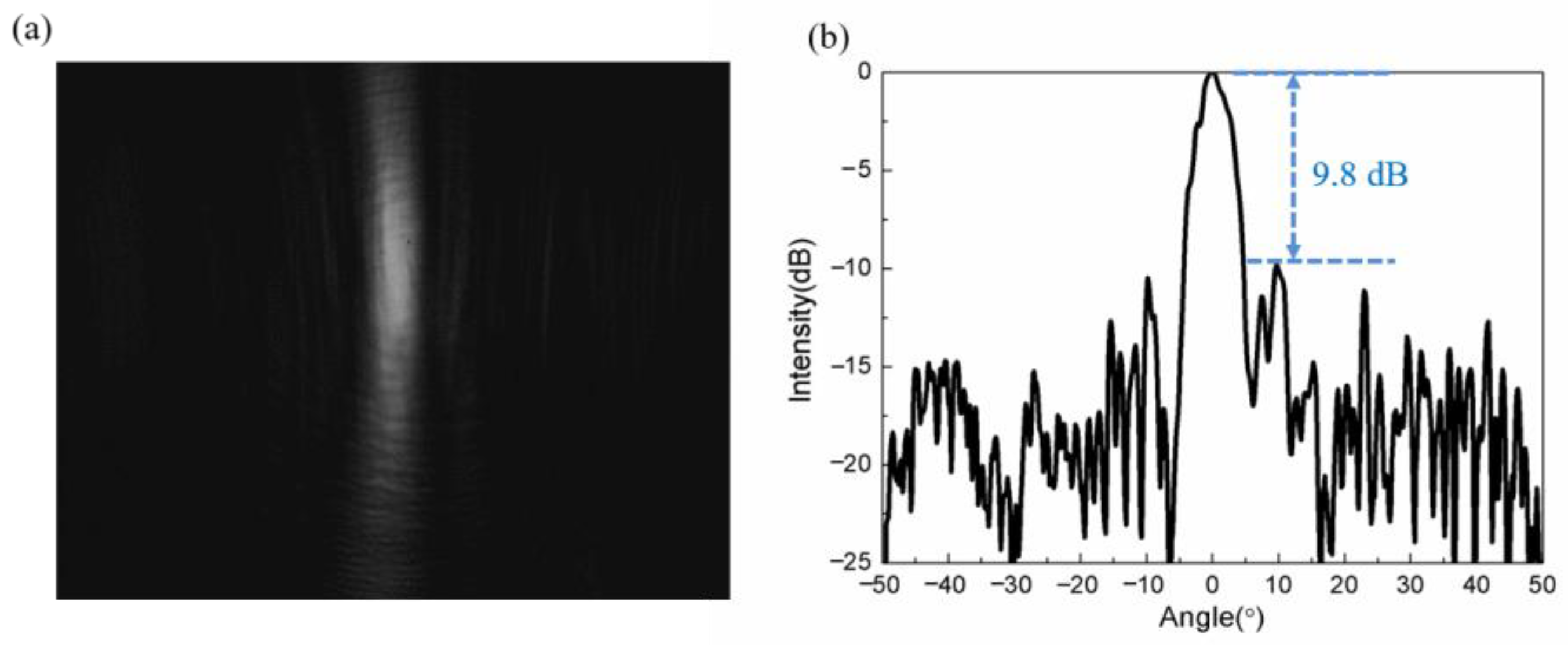
Different optical waveguide widths and fabrication errors of waveguides result in an optical phase mismatch among the antennas; thus, the field distribution is random without external voltage applied. The hybrid-integrated OPA is placed in the center of the FOV of the imaging system. To compensate the stochastic phase error induced in the waveguide array due to fabrication error, the stochastic parallel gradient descent (SPGD) algorithm is used to optimize the drive voltages for phase calibration and beam steering. After fine compensation for the phase mismatch with applied voltage, the beam is calibrated well, as shown in
Figure 8a.
Figure 8b shows the normalized intensity of the far-field beam distribution after phase compensation. The side-lobe suppression ratio is about 9.8 dB, slightly different with the simulated ones, which may be caused by the background noise and the precision of the voltage.
The measured beam intensities at different steering angles in the far-field are shown in
Figure 9. The maximum steering angle is measured to be ±25°, which is limited to the integrated laser power and the detection limitation of the optical detection system. A more accurate control algorithm and a higher precision in the voltage should be used to steer the beam towards large angles with lower side-lobe noise in the future.
The results show that the proposed hybrid-integrated strategy can efficiently integrate the III–V-based DFB laser source and the silicon-based OPA chip. Compared with the monolithically heterogeneous integration of laser and modulators [
12,
13,
14], the hybrid integration process has a large tolerance and is cost-effective. The measured results of the beam steering show that there is a good coupling efficiency in the grating coupler and that there is only single main beam in the far-field, which is grating lobe-free. The integrated chip enables the LiDAR to move towards miniaturization, an all solid-state and a low-cost [
17]. In the future, the source power could be further improved or amplified using an erbium-doped waveguide [
18]. It is essential that the insertion loss of the on-chip OPA should be decreased for low-loss beam steering (including the loss of the grating coupler, power splitter and optical antenna). The measured coupling loss of the grating coupler for the integration of OPA and the laser chip could be improved with higher fabrication precision. The butt coupling-based antenna could be further improved using the tapered waveguide, which can reduce the reflection of the end face and increase the optical transmission. For 2D beam steering, the antenna array could also be arranged with a 2D nano-antenna array [
19,
20].
