Article

Theoretical and Experimental Study of Optical Losses in a Periodic/Quasiperiodic Structure Based on Porous Si-SiO2

by
María R. Jiménez-Vivanco
1,*,
Raúl Herrera
1,
Lizeth Martínez
2,
Francisco Morales
3,
Khashayar Misaghian
4,5,
Miller Toledo-Solano
6 and
J. Eduardo Lugo
4,5,7,*
1
Instituto de Física, Universidad Nacional Autónoma de México (UNAM), Circuito de la Investigación Científica, Ciudad Universitaria, Mexico City 04510, Mexico City, Mexico
2
Tepeji Graduate School, Industrial Engineering, Autonomous Hidalgo State University, Av. del Maestro No. 41, Col. Noxtongo 2ª Sección, Tepeji del Rio 42855, Hidalgo, Mexico
3
Optics Research Center, A.C., Loma del Bosque 115, Col. Lomas del Campestre, León 37150, Guanajuato, Mexico
4
Faubert Lab, School of Optometry, University of Montreal, Montreal, QC H3T1P1, Canada
5
Sage-Sentinel Smart Solutions, 1919-1 Tancha, Onna-son, Kunigami-gun, Okinawa 904-0495, Japan
6
CONAHCYT-Facultad de Ciencias Físico-Matemáticas, Benemérita Universidad Autónoma de Puebla, Av. San Claudio y Av. 18 Sur, Col. San Manuel, Ciudad Universitaria, Puebla 72570, Puebla, Mexico
7
Facultad de Ciencias Físico-Matemáticas, Ciudad Universitaria, Puebla 72570, Puebla, Mexico
*
Authors to whom correspondence should be addressed.
Photonics 2023, 10(9), 1009; https://doi.org/10.3390/photonics10091009
Submission received: 4 July 2023 / Revised: 21 August 2023 / Accepted: 29 August 2023 / Published: 4 September 2023
(This article belongs to the Special Issue Group IV Photonics: Advances and Applications)

Abstract

:
This study investigates the reduction of optical losses in periodic/quasiperiodic structures made of porous Si-SiO2 through a dry oxidation process. Due to their unique optical properties, these structures hold great promise for various optoelectronic applications. By carefully engineering the composition and geometry of the structures, we fabricate periodic/quasiperiodic structures on a quartz substrate using an electrochemical anodization technique and subsequently subject them to dry oxidation at two different temperatures. The structure exhibits two localized modes in the transmission and reflection spectra. Unoxidized and oxidized structures’ complex refractive index and filling factors are determined theoretically and experimentally. Optical characterization reveals that the porous Si-SiO2 structures exhibit lower absorption losses and improved transmission than the pure porous silicon structures. Additionally, scanning electron microscopy (SEM) and energy-dispersive X-ray spectroscopy (EDS) confirm the presence of porous Si-SiO2 and reduced silicon content. Our study demonstrates that dry oxidation effectively decreases Rayleigh scattering losses, leading to enhanced optical performance and potential applications in efficient optoelectronic devices and systems based on silicon. For instance, periodic/quasiperiodic structures could soon be used as light-emitting devices inside the field of optoelectronics, adding photoluminescent nanoparticles to activate the localized modes.

1. Introduction

In the realm of optical science and engineering, the manipulation of light has paved the way for extraordinary advancements, shaping the very foundation of modern technology. Central to these advancements are periodic and quasiperiodic structures (PQS), which exhibit fascinating optical properties that have captivated researchers for decades. Periodic and quasiperiodic structures have gathered significant attention in modern science and engineering due to their diverse applications in communication, medical diagnostics, gas sensors, photoluminescent bio-imaging, and drug delivery systems [1,2,3,4]. These structures’ ability to control and harness light is paramount in many applications, as evidenced by the current technologies and devices that rely on their ingenious designs, such as ultra-efficient solar cells and high-capacity optical communication to exceptional lasers and photonic devices. The metamaterial-based perfect absorbers are groundbreaking technology that utilizes periodic/quasiperiodic structures [5]. These absorbers are engineered to capture and convert a specific range of incident light into helpful energy with remarkable efficiency.
By carefully tailoring the geometry and composition of the structures, researchers have developed solar cells that can absorb light across a broad spectrum and, thus, exhibit significantly improved energy conversion rates compared to conventional photovoltaic systems. This innovation holds tremendous promise for sustainable energy solutions, ushering in an era of highly efficient solar energy harvesting. In the field of high-speed data communication, periodic structures find applications in photonic crystals [6]. These crystals possess periodic variations in refractive index, enabling them to control light propagation at the nanoscale level. By manipulating the flow of photons, photonic crystal fibers have been created to carry and guide light signals with minimal loss, revolutionizing optical communication by providing faster and more reliable data transfer rates. This technology underpins the backbone of modern Internet infrastructure and data centers, serving as a vital component in our increasingly interconnected world. Another remarkable application of periodic/quasiperiodic structures is the development of advanced optical sensors [7]. By carefully engineering the properties of these structures, researchers have designed highly sensitive and selective sensors capable of detecting minuscule amounts of specific substances. These sensors are instrumental in various industries, from environmental monitoring to medical diagnostics, empowering us to detect pollutants, pathogens, and hazardous chemicals with unprecedented accuracy and speed. Moreover, periodic and quasiperiodic structures have found their way into lasers and light sources [8]. Photonic crystals and random lasers incorporate these structures and have demonstrated superior efficiency, output power, and beam quality performance. These lasers can potentially drive significant advancements in material processing, medical surgery, and fundamental research.
These structures, mainly when based on porous silicon (PS), exhibit unique optical properties that have proven invaluable in many fields. However, studying optical losses in these structures, arising from absorption and Rayleigh scattering remains critical for their practical implementation and optimization in optoelectronics and beyond. While periodic/quasiperiodic structures have demonstrated impressive capabilities in communication and medical applications, their potential utilization in optoelectronics and battery technologies has been hindered by the adverse effects of oxidized PS on material performance [9].
Oxidation, a ubiquitous PS phenomenon, changes the material’s optical parameters, porosity, thickness, and pore size [10,11]. It is well known that PS multilayers can oxidize when exposed to oxygen [12,13]. A chemical reaction of PS with the oxygen in the air forms an oxide on the PS surface, interfaces, and pores walls [10,14]. These alterations significantly influence the optical losses and ultimately impact the quality and efficacy of optical structures in the visible and infrared regions [15]. Understanding and controlling the oxidation process is essential in achieving desired optical properties in periodic/quasiperiodic systems.
Optical losses in these structures are mainly attributed to absorption and Rayleigh scattering [16,17]. While Rayleigh scattering dominates in the infrared region due to the transparency of silicon at those wavelengths [18], absorption losses play a more critical role in the visible region [15]. Moreover, imperfections in the PS structure, such as roughness, introduce light scattering, which affects the transmission of light and can compromise the performance of optical devices [19]. Since roughness is always present in a multilayer structure, its spectral position, photonic bandwidth, and optical quality can be affected by scattering losses [20].
Therefore, managing optical losses caused by absorption and scattering becomes paramount for enhancing the efficiency of periodic/quasiperiodic structures. Addressing the scattering losses in these structures is a challenging yet vital endeavor. Studies have shown that refractive index perturbations can lead to scattering, increasing cavity loss rates and impacting the spatial emission profile of excited atoms within a cavity [21]. The influence of sidewall roughness on optical losses has been demonstrated, reducing scattering effects as a critical factor in achieving high-quality optical structures [22,23]. In p-type silicon substrates, the optical losses in a waveguide are due to free carrier absorption more than surface scattering losses or volume scattering [24]. The optical response of a porous structure can be enhanced if it has a smooth surface. Therefore, many authors exposed that the optical losses by scattering can be reduced when PS is subjected to thermal oxidation given place to smooth surface in the PS structure [25]. Also, it has been found that the transformation of PS to porous Si-SiO2 strongly decreases the absorption coefficient of Si [26,27]. Techniques such as low-temperature anodization and precise control of the oxidation process have shown promise in reducing fluctuations and enhancing optical properties [28,29]. This result is of importance because it has been reported that the scattering effects are amplified by a higher number of interfaces, which causes a stronger light scattering, limiting the quality of the optical structures [29], but using an electrolyte viscosity or applying an oxidation process is the key to reduce the roughness and obtain smoother PS structures with several interfaces [29,30].
In this context, the present study aims to investigate the reduction of optical losses in a periodic/quasiperiodic structure made of porous Si-SiO2. We employ an accessible and economical oxidation method to minimize Rayleigh scattering and absorption losses, explicitly targeting the structure’s two localized modes (LM). The findings of this research shed light on the potential of porous Si-SiO2 as a promising candidate for advanced optoelectronics and related applications. By analyzing the effects of oxidation conditions on the optical response, porosity, and surface smoothness, this work presents a significant advancement in the understanding and practical implementation of periodic/quasiperiodic structures for optical applications.
This study shows that the Rayleigh scattering losses of the porous Si-SiO2 structure decreased by more than 47% at the first LM, and at the second LM decreased by 57% compared with the photon losses of the PS structure. In addition, the Si-SiO2 structure remains porous even after applying a high oxidation temperature. Also, we can observe an increase in the transmission amplitude after dry oxidation, a change in the wavelength position of both LMs, and an increase in the resonance bandwidth of both LMs.
In summary, reducing optical losses in periodic/quasiperiodic structures is crucial for unlocking their full potential in optoelectronics and various other fields. This study presents a novel approach to minimize Rayleigh scattering and absorption losses, offering a pathway toward developing efficient, high-performance optical devices and systems based on silicon.

2. Materials and Methods

2.1. PQS Complex Refractive Index

It is well known that a complex refractive index can be obtained by applying the effective medium approximation using Maxwell Garnett, Looyenga, and Bruggeman equation [31,32]. However, in this work, we used the Maxwell Garnet and J.E. Lugo model to find the theoretical complex refractive index of PS and porous Si-SiO2 [33]. Since the Looyenga and Bruggeman equation overestimates the refractive index value for PS, the Maxwell Garnett equation was chosen to obtain the refractive index of PS in this work [31].
Maxwell Garnett’s equation for two mediums is written as follows:
ε P S ε S i ε P S + ε S i = P ε a i r ε S i ε a i r + ε S i ,
where P (porosity) is the air fraction of the silicon matrix, ε a i r is the dielectric constant of air, ε S i is the dielectric constant of Si, and ε P S is the effective dielectric constant of PS. So, the refractive index of PS is expected to be lower than that of Si because PS is a mixture of air and the solid phase of Si.
On the other hand, we selected the J.E. Lugo model to calculate the refractive index of porous Si-SiO2 because it predicts less absorption at short wavelengths compared to the two models mentioned above [15]. This model is an extended version of Maxwell Garnett, which includes three mediums: Si, SiO2, air, and the oxide fraction and its network expansion within the silicon matrix.
The following equation can calculate the complex refractive index of three mediums:
ε O P S ε S i ε O P S + ε S i = P * ε 1 * ε 3 * ε 1 * + ε 3 *
where ε 1 * and ε 3 * are given by
ε 1 * = ε a i r 1 + ε SiO 2 ε a i r γ
ε 3 * = ε S i 1 + ε air ε SiO 2 γ
where γ = 1 β 1 + β , ε SiO 2 represents the dielectric constant of SiO2 and ε O P S is the dielectric constant of porous Si-SiO2.
In Equation (2), P * = P o x β and P o x is the porosity of the system of three mediums.
Therefore, β is represented by
β = 1 0.55 x 1 + 0.45 x 2 ,
where x is a dimensionless oxidation parameter. The constants 0.55 and 0.45 are related to oxide growth in Si. So, an oxide layer grows 55% above the Si wafer and 45% below the original surface. Thus, the Si is consumed as the oxide increases, and a volume expansion occurs during oxidation.
The porosity for a system of three mediums can be calculated as
P o x = P 1 0.55 x 2
The oxidation parameter’s upper limit value, x L , is determined by solving the following equation:
P 1 + 0.9 x L + 0.2015 x L 2 1 .
Taking into account all the parameters mentioned above, it is possible to calculate the oxide fraction of porous Si-SiO2 layers as
f o x = P 2 x 0.1 x 2 .
Therefore, the Si fraction f s i can be obtained by the following equation:
f s i = 1 P o x f o x .

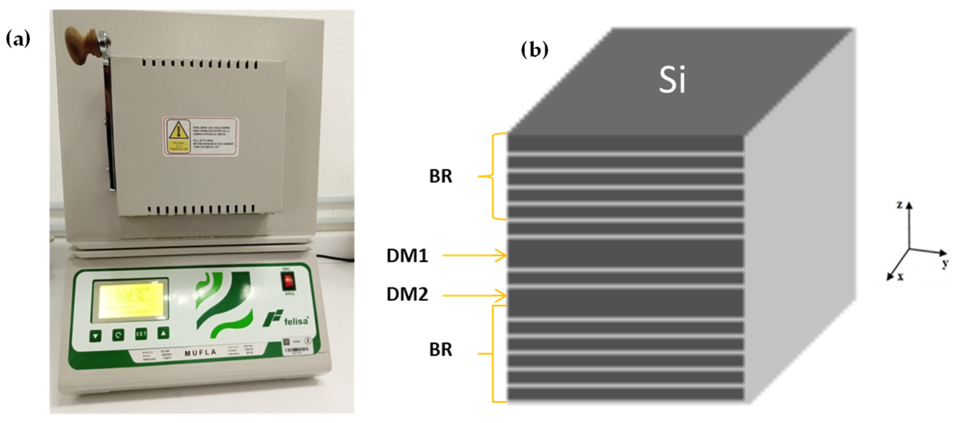
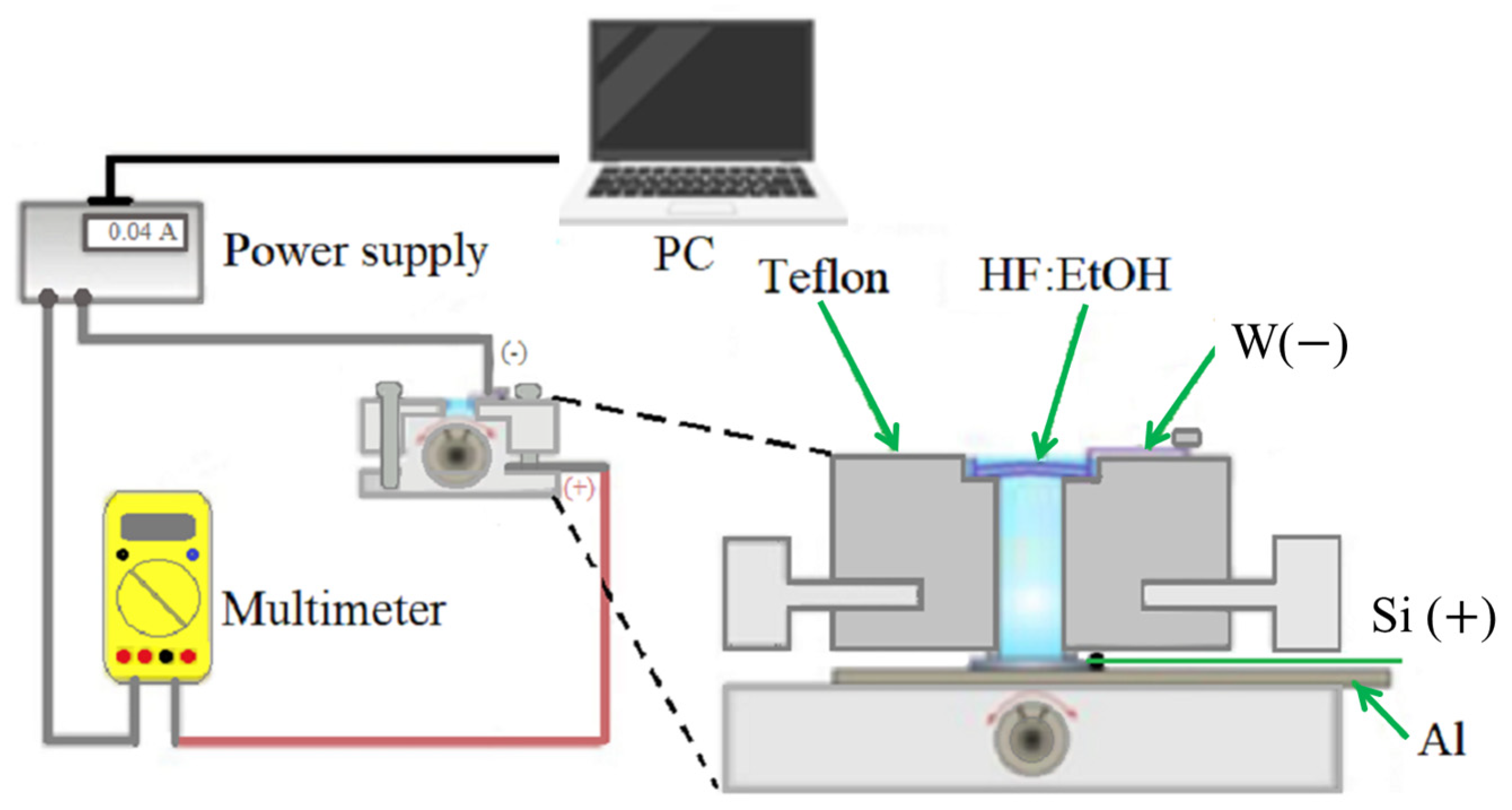
2.2. Porous Silicon Periodic/Quasiperiodic Structures Fabrication

PS PQS was obtained by electrochemical anodization on silicon (Si) wafers, type p+, 0.01–0.02 resistivity, (100) orientation. The Si wafer was put in a Teflon cell with an etching area of 1.1 cm2 that was used to carry out the electrochemical process; after, an aqueous solution based on 40% HF and ethanol at 99.7% with a volume relation of 1:1 was placed in the Teflon cell.
During the anodization process, two alternating current densities (80 mA/5 mA) were applied using a power supply (Keysight B2961A, Penang, Malaysia) controlled by a laptop. The existing profile consisted of 15 periods that correspond to low/high refractive index (nL/nH) and high/low current densities (80 mA/5 mA); the first five periods (nL/nH)5 were used to make up a Bragg reflector (BR); then, a Fibonacci sequence (nL/nH) (nH/nL) (nH/nL) (nH/nL) of four order follows. Finally, a BR with six periods (nL/nH)6 was fabricated to complete the final structure. The anodization time for thickness growth to the first and second layers was 1.53 s (s) and 6.31 s (s). So, two LM were created between two BRs, an essential characteristic of a PQS, where the light is confined. Furthermore, the PQS was self-supported on a quartz substrate. The PQS lifting was carried out using the same electrolyte mentioned above, where a high current pulse of 450 mA/cm2 was applied for 2 s to the c-Si substrate. Finally, the electrolyte was removed from the Teflon cell, adding three times ethanol to the solution, so the sample was removed and placed in a Petri box with ethanol; the sample was put on the quartz substrate and dried at room temperature. Figure 1 exhibits the electrochemical etching setup and various parts of the etching cell used to fabricate PS PQS.

2.3. Porous Si-SiO2 PQS Fabrication

Further, with the idea of manufacturing PQS based on porous Si-SiO2, we employed an electric muffle to carry out the oxidation process, where the temperature and oxidation time were modified. The oxidation process involves applying two stages of dry oxidation, the first based on a low temperature at 350 °C for 30 min and the second stage using a high temperature at 800 °C for 30 min.
In the second step of dry oxidation, the muffle temperature arrives from 350 °C to 800 °C in 17 min, and then the second step of dry oxidation is started for another 30 min; this occurs when the system is set to a temperature of 800 °C. Figure 2a,b shows the muffle furnace used to carry out the oxidation process that converted the PS into porous Si-SiO2 and the schematic illustration of PQS, which is made up of a quasiperiodic structure between two BR, there can be seen two defect modes (DM1 and DM2) where the light is confined.

2.4. PQS Optical Characterization

The optical characterization of the PQS was carried out before and after dry oxidation with a Cary 5000 UV-VIS-NIR spectrophotometer (Agilent Technologies, Penang, Malaysia) with a halogen lamp source at an incidence angle of 8° for reflection measurements and 0° for transmission measurements from 200 to 800 nanometers.
Theoretical transmission and reflection spectra were obtained using the matrix method [15]. The Transfer Matrix Method can obtain light propagation through a PQS of PS and porous Si-SiO2. It can be resolved for N numbers of layers and can be calculated by
M 11 M 12 M 21 M 22 = D 0 1 l = 1 N D l P l D l 1 D S ,  
where M 11 , M 12 , M 21 , and   M 22 are matrix elements; they are fundamental to describing how electromagnetic waves propagate along a medium; D l is the dynamical matrix of PS o porous Si-SiO2, D 0 is the dynamical matrix of air, and D s is the dynamical matrix of the substrate in both cases we have quartz substrate and, finally, P l is the propagation matrix.
To obtain the transmission and reflection, we employed the following equation:
T = n s cos θ s n 0 cos θ 0 1 M 11 2 ,
R = M 21 M 11 2 ,
where T represents the transmission, n s is the substrate’s refractive index, n 0 is the refractive index for air, θ s is the substrate’s output angle, θ 0 is the incidence angle, and R is the reflection.
From this approach, it is also possible to estimate the individual thicknesses (dH and dL) of the PQS by adjusting the transmission and reflection spectrum once the complex refractive index values are inferred.

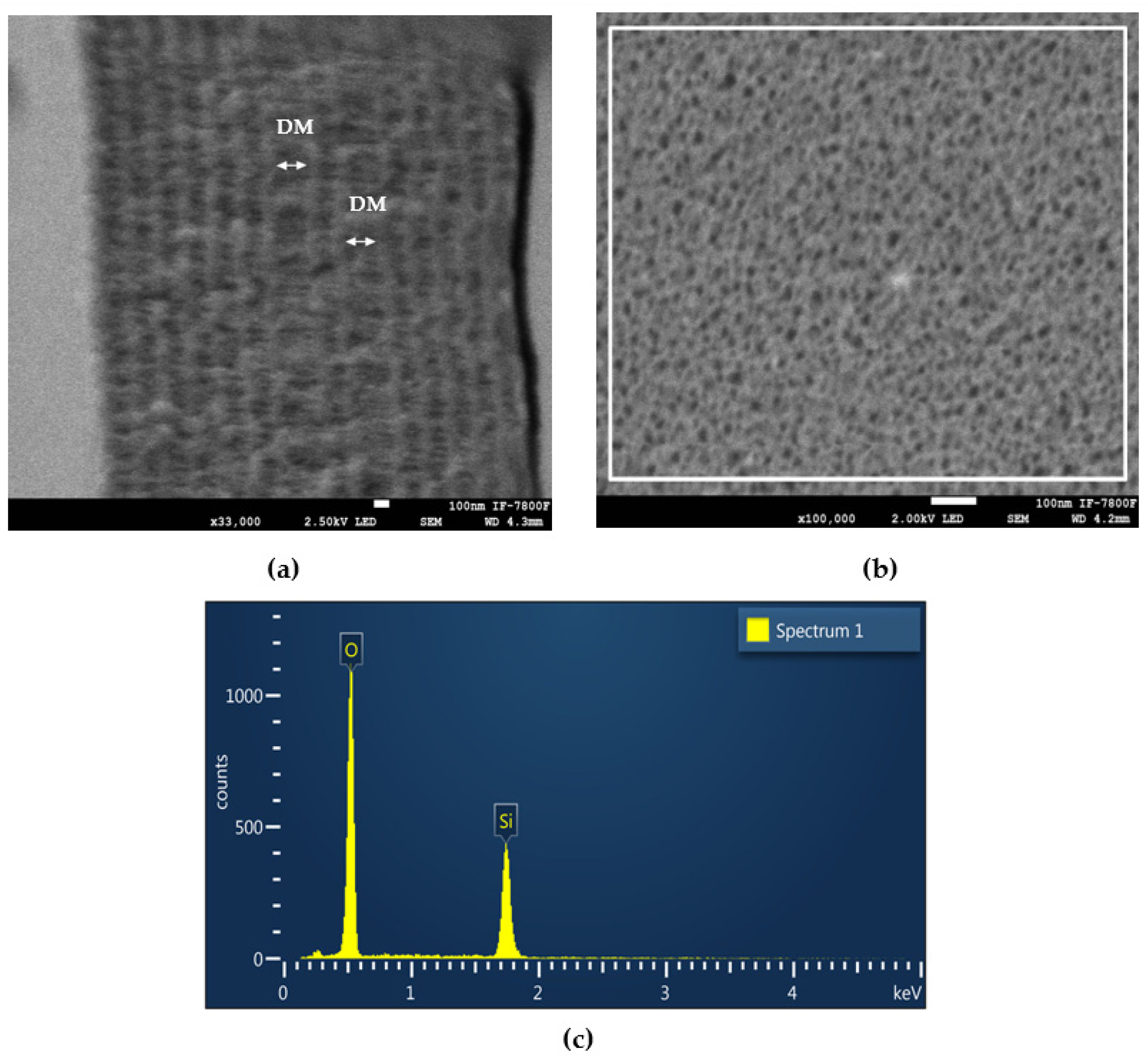
2.5. Porous SiO2 PQS SEM and EDS Characterization

Additionally, a (JEOL FE-SEM JSM-7800, Tokio, Japan) obtained the morphology of the porous Si-SiO2 structure. Taking the cross-section SEM (z-direction in Figure 2) allows for extracting the number of layers and thicknesses. The pore diameter can be inferred by superficial-section SEM (xy-plane in Figure 2). Moreover, the SEM microscope can characterize chemically using energy-dispersive X-ray spectroscopy (EDS). We used that feature to quantify the amount of Si and oxide in the porous Si-SiO2 structure.

2.6. Optical Losses

2.6.1. Absorption Losses

The absorption spectrum of PQS can be inferred using the transmission spectra, and Beer’s Lambert law. This can be calculated using the following equation:
A = l o g 10 1 Τ ,
where A is the absorption and Τ represents the transmission. Thus, this equation is related to the light intensity that passes through the PQS, where a fraction of light is absorbed and the other is transmitted.

2.6.2. Scattering Losses

Also, we made a theoretical analysis of the optical losses at the wavelength of the two LM in a PQS. For that, we employed the modified Breit–Wigner expression, obtained by one of us [15,34,35] to estimate the lifetime of photons and photon losses (Rayleigh scattering) before and after dry oxidation. So, we applied the modified Breit–Wigner expression to adjust the experimental transmission spectrum at the wavelength of the two LM as an energy function. The Rayleigh scattering analysis is achieved by a quantum mechanical model proposed by Miller [15,34,35]. The model estimates the optical losses by Rayleigh scattering before and after dry oxidation at the wavelength of two LM in a PQS.
Here, the porous structure disorder allows the estimation of the total rate of Rayleigh scattering. This model treats the features of the PS structure as a conglomeration of crystalline Si wires with a typical radius a and length a ; branches begin to have fluctuations and move away from a cylindrical shape [15,34,35]. Due to these fluctuations in the dielectric constant, the Rayleigh scattering is an important parameter as a medium of energy loss [15]. In this model, the parameters a should be smaller than the period of the Bragg mirrors, that is, a < d H , d L [15,35].
The equation of Breit–Wigner modified by Miller is closely related to the transmission spectra for each LM. This equation is represented by
T ω = Γ 2 Γ + Γ p 2 + ω ω 0 2 ,
where Γ is the lifetime at the wavelength of the light LM due to the finite probability of tunneling through the BR, Γ p represents the photon loss rate in the PQS. In contrast, the lifetime can be defined at the wavelength of the LM as τ = 1 Γ p , on this, the Rayleigh scattering losses and absorption losses are included.
The volume-averaged fluctuation of porous silicon and porous Si-SiO2 dielectric constant is well approximated by
δ ε 2 V = 16 p 1 p ε 2 ε 1 2 a 2 a ,
where ε 1 and ε 2 are the minimal and maximum dielectric constant bound of the porous and solid phase regions (Si and Si-SiO2), respectively. For PS, ε 1 = 1 and ε 2 = 12 , and porous Si-SiO2 is ε 1 = 1 and ε 2 = 3.9 . p is the mean porosity of the PS (P) or porous Si-SiO2 (Pox) structures.
The Rayleigh scattering losses (RSL) can be obtained as
α R S L = Γ R S L c = π δ ε 2 V ω 0 2 6 ε * 2 c D ω 0 ,
where Γ R S L represents the Rayleigh scattering loss rate in the PQS, ω 0 is the angular frequency of the position of each LM, c is the speed of light, and D ω 0 is the density of photon states in the Bragg reflector given by D ω 0 = ε * 3 2 ω 0 2 π 2 c 3 , which is close to the density of states in uniform media with the dielectric constant ε * expressed as
ε * = d H ε H + d L ε L Λ ,
where d H is the high porosity layer thickness, d L is the low porosity layer thickness, and Λ is the period Λ = d H + d L , ε H and ε L correspond to the dielectric constants of porous silicon or porous Si-SiO2 layers; ε H = n H 2 for low porosity and ε L = n L 2 for high porosity layers.

3. Results and Discussion

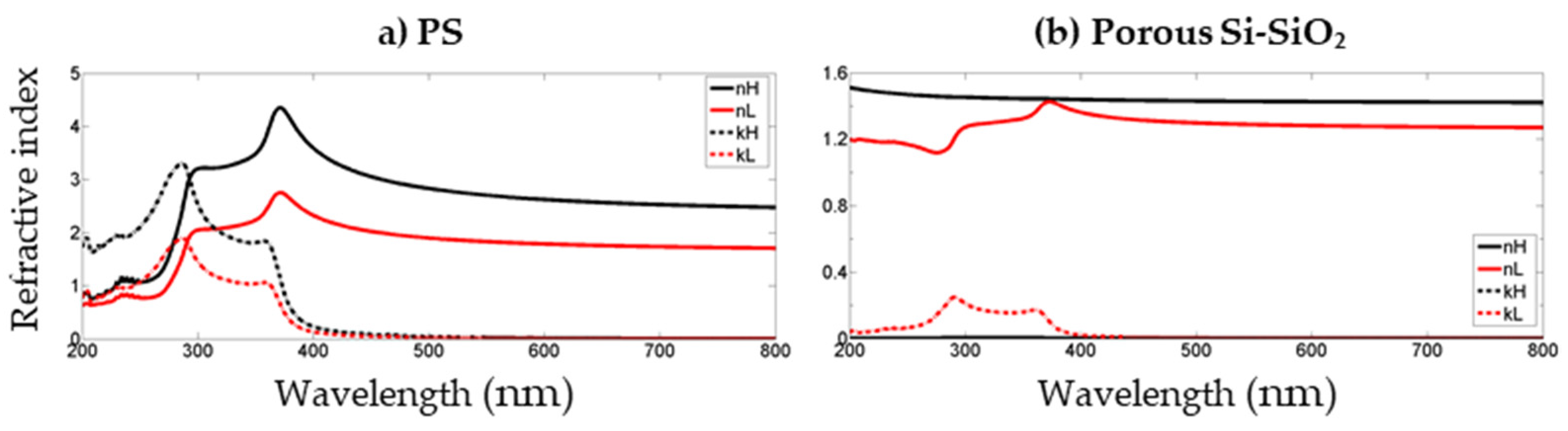
3.1. PQS Complex Refractive Index

The complex refractive index of PS and porous Si-SiO2 results are shown in Figure 3a,b. The red lines indicate high porosity refractive indexes (nL), and the black lines the low porosity refractive indexes (nH). The dotted lines correspond to the extinction coefficient (k), the imaginary part of n. The dotted red lines indicate high porosity extinction coefficients (kL), and the dotted black lines the low porosity extinction coefficients (kH). As you can observe in Figure 3b, both the low and high porosity refractive indexes decreased after dry oxidation compared to the PS refractive indexes (Figure 3a). Additionally, the k becomes zero for the high porosity layers (Figure 3b).
Also, we can see the value of the high refractive index of porous Si-SiO2 corresponds to the refractive index of silicon dioxide (SiO2). The J.E. Lugo model predicts that our structures are almost made up of SiO2.
Table 1 displays the periodic/quasiperiodic structure refractive indexes and filling factors before and after dry oxidation. We use the average of both LM wavelengths to obtain the complex refractive index before and after oxidation. Again, it is shown that the refractive index of porous Si-SiO2 is smaller than the refractive index of PS; this is because a part of Si with a refractive index equal to 3.5 is replaced by SiO2 (refractive index 1.4) and SiO2 occupies a part of the air. So, when SiO2 consumes the Si, the silicon’s refractive index tends to decrease.
Also, the porosity before and after dry oxidation (P and Pox) was calculated, where it was found that after dry oxidation, part of the air is replaced by SiO2, reducing the pore size and porosity. Thus, PS remains porous even after applying a high oxidation temperature.

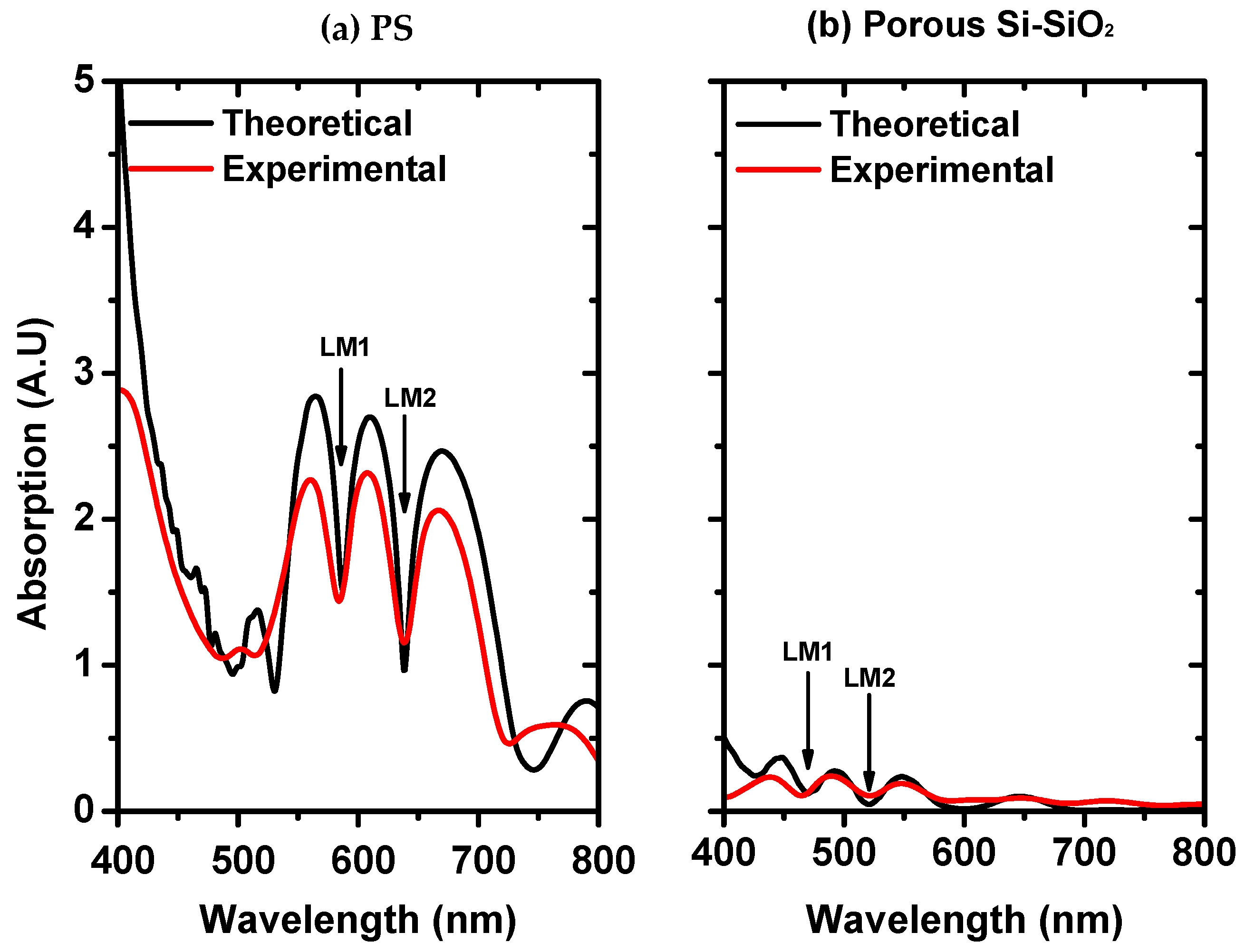
3.2. PQS Optical Characterization

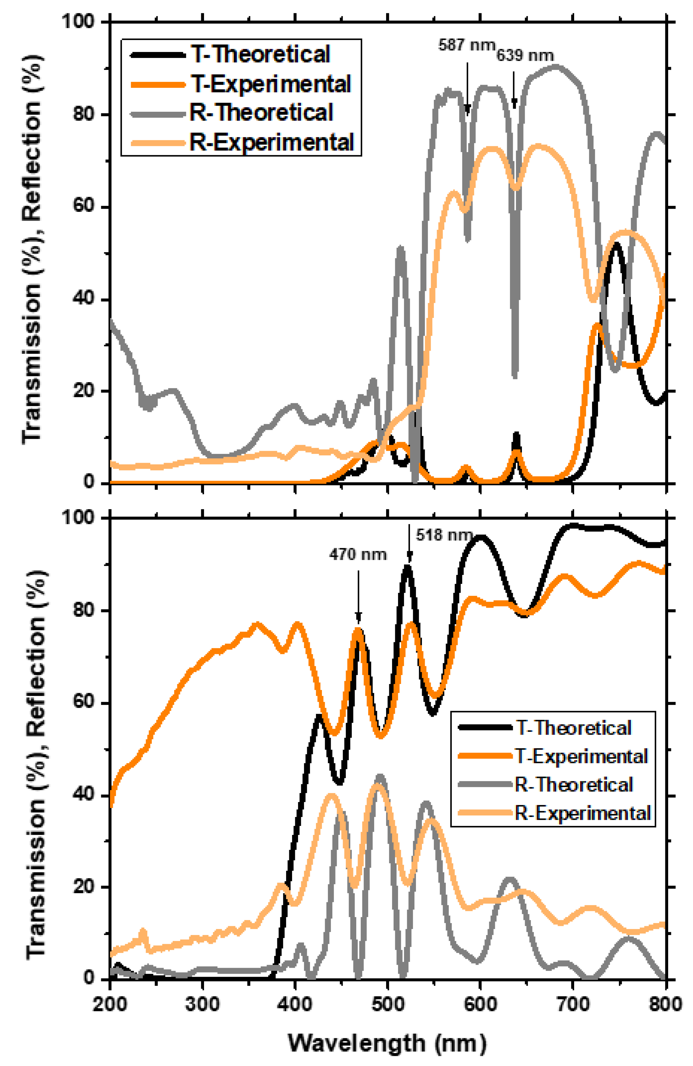
Porous Si-SiO2 PQS Transmission and Reflection Spectra

Figure 4 displays the theoretical and experimental transmission and reflection spectra of a PQS manufactured of PS and porous Si-SiO2, which was placed on a quartz substrate. The high and low porosity values used to fit the theoretical transmission and reflection spectra of PS were 75% and 44%.
In Figure 4 (top), the PS-PQS shows two LM in the transmission and reflection spectra at 587 and 639 nm wavelengths. Theoretical and experimental results showed a good fit. Also, in Figure 4 (top), PS-PQS transmits close to 5% of the light and 10% for the first and second LM, whereas the reflected light at the same LM wavelengths is 55% and 25%. As you can see, in the UV region, the transmission and reflection are almost zero. This is due to optical losses by scattering and absorption of light in PS.
Figure 4 (bottom) shows the theoretical and experimental reflection and transmission spectra of porous Si-SiO2 PQS, where can be observed two LM positioned at 479 and 518 nm as you can follow, theoretical and experimental transmission and reflection spectra of porous Si-SiO2 match very well. Also, it is exhibited that absorption losses decreased after dry oxidation. For this reason, the transmission spectra of porous Si-SiO2 increased from 5% to 70% for the first LM and from 10% to 70% for the second LM. Additionally, a wavelength shift of 117 nm and 121 nm for the first and second LM is detected; the wavelength shift is due to a decreased refractive index by introducing SiO2 into the PS matrix, which has a refractive index lower than the silicon.
Moreover, the porous Si-SiO2 transmission spectrum exhibits a more significant bandwidth narrowing than the PS transmission spectrum due to decreased refractive index contrast (see Table 1).
The periodic/quasiperiodic structure thicknesses before dry oxidation inferred from the optical measurements were dL = 85.59 nm and dH = 58.83 nm.

3.3. Porous Si-SiO2 PQS SEM and EDS Characterization

Figure 5a,b exhibits the SEM images of the cross-section and superficial section of an oxidized PQS on a quartz substrate. Cross-section SEM measurement displays the two defect modes (white arrows) between two BR introduced in the porous structure on a quartz substrate. The layers with low porosity can be observed in light gray, and layers with high porosity are displayed in dark gray. The structure manufactured in Figure 5a has the following sequence (nL/nH)5 (nL/nH) (nH/nL) (nH/nL) (nH/nL) (nL/nH)6. Conversely, superficial-section SEM shows the pore diameter and the wire thicknesses of a porous Si-SiO2 PQS, showing that the structure remains porous after dry oxidation.
According to the SEM measurements, the periodic/quasiperiodic structure thicknesses after dry oxidation are dL = 103 nm and dH =76.8 nm. Thus, the thicknesses of porous Si-SiO2 PQS are more considerable than PS PQS thicknesses.
To be sure that porous Si-SiO2 PQS was made up, EDS measurements were taken, where we can quantify the amount of Si and oxide in the porous Si-SiO2 structure. Figure 5c shows that the oxide amount is more significant than the Si amount. So, we confirmed that a porous Si-SiO2 structure is formed. The white rectangle in Figure 5b displays the selected area taken to obtain the EDS measurements.
Table 2 displays the quantification results obtained by EDS, indicating that oxygen and Si form the porous structure with a percentage of silicon mass of 48.94% and oxygen of 51.06%. Stoichiometry silicon dioxide has a percentage of the silicon mass of 47% and 53% oxygen. Consequently, there is still, on average, a 1.94% silicon remaining within the structure. This value supports the results shown in Table 1, where we found that f s i is less than 3%.

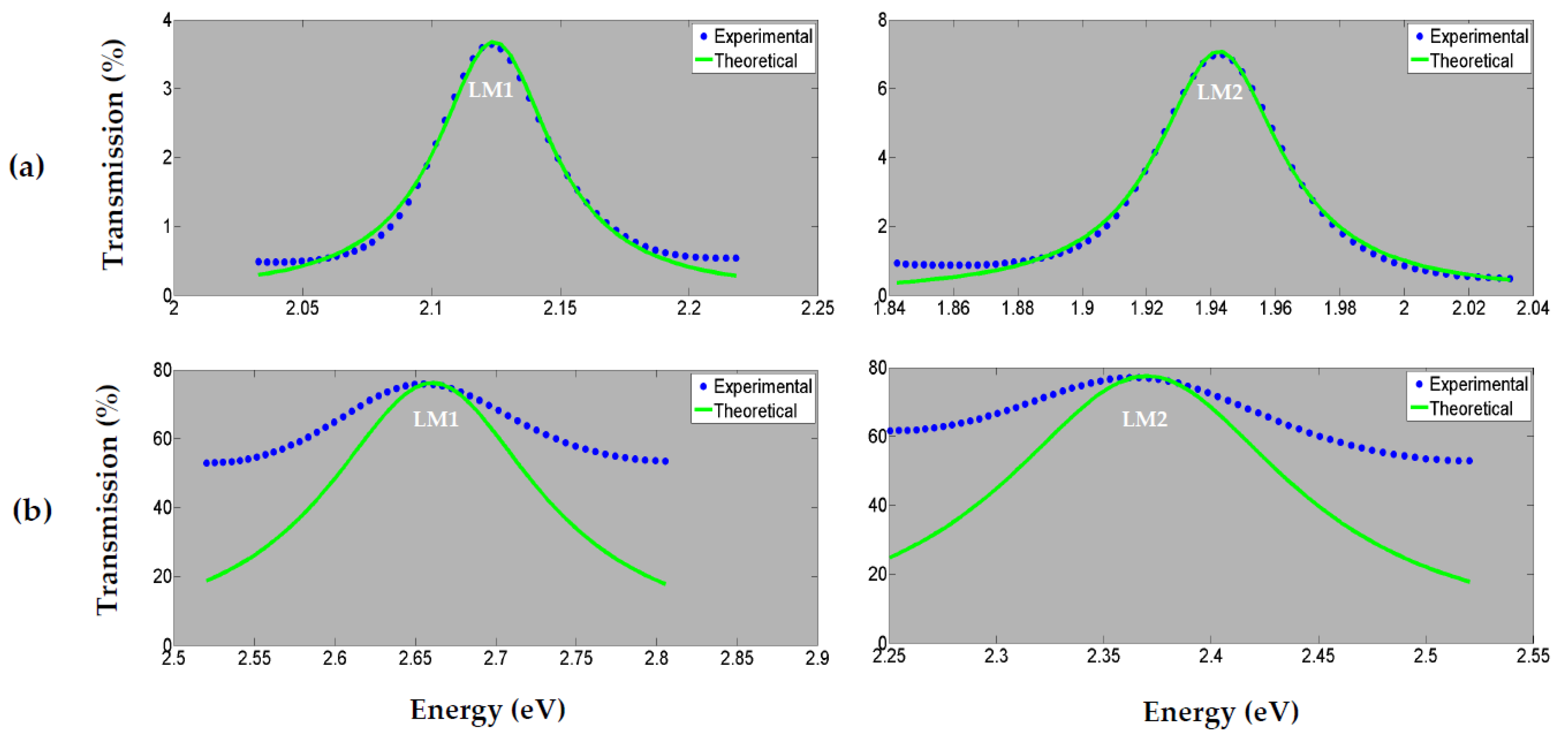
3.4. PQS Optical Losses

Periodic/quasiperiodic structures designed in the infrared have been studied [36,37], where PS structures are considered a material without optical losses. However, it has been demonstrated that light scattering by the pores and the interfaces between layers play a much more critical role than the infrared region’s light absorption [38] since the extinction coefficient of crystalline silicon tends to zero [39]. Therefore, in the UV-VIS region, both loss mechanisms must be considered [15].
Also, it has been reported that to achieve the same degree of performance in the visible range and the infrared region, the layers of higher porosity are required to reduce the value of k further, thus blue-shifting the absorption edge [40]. Still, it is challenging since thin crystalline silicon wires can be broken due to feeble mechanical resistance and usually crack during drying [29].
On the other hand, it has been demonstrated that optical losses in a UV free-standing microcavity can be reduced by SiO2 addition, given mechanical stability to the porous structure [15]; this occurs because a thick wire of Si-SiO2 was created. For this reason, we studied the optical losses in a periodic/quasiperiodic structure made up of PS and porous Si-SiO2 in the visible region to archive porous structures with high quality and lower optical losses.

3.4.1. PQS Absorption Losses

First, we studied the optical losses by absorption in the PS and porous Si-SiO2 PQS. Figure 6 exhibits the theoretical and experimental absorption spectra of a PQS made of PS and porous Si-SiO2. In both plots, the black line corresponds to the theoretical absorption, and the red line is the experimental absorption for a PQS of PS and porous Si-SiO2, respectively. The PS PQS absorption spectra are displayed in Figure 6a, whereas the porous Si-SiO2 PQS absorption spectra are shown in Figure 6b. As you can observe, the porous Si-SiO2 structure presents fewer absorption losses than the PS structure. Additionally, the first LM1, in both cases, has more absorption losses than the second LM2, which is found at longer wavelengths; LM1 and LM2 are exhibited as an absorption minimum in Figure 6. Adding oxide to the PS structure reduced the optical losses by absorption. The theoretical and experimental absorption spectra match very well in both cases.

3.4.2. PQS Scattering Losses

Scattering effects can be observed in Figure 7. Before dry oxidation, the maximum amplitude of the transmission spectrum at the wavelength of the first and second LM is 4% and 8%. However, after dry oxidation, an increase in the amplitude, a change in the position of both modes, and an increase in the resonance wavelength bandwidth at the wavelength of the two LM are found.
In Table 1, we calculated the silicon fractions (fsi); it was estimated to be less than 3% in the porous Si-SiO2 structure, and from EDS, the estimated remaining crystalline silicon is 1.4%. This demonstrates that optical losses by absorption can be neglected due to the smaller amount of Si in the porous Si-SiO2 structure. Thus, all the optical losses are due to Rayleigh scattering in the visible region. Taking into account the results shown in Table 3 and Table 4, which were obtained by applying the quantum mechanical model described in [15,34,35], we could demonstrate that the Rayleigh scattering levels are lower at the two LM positioned at 470 and 518 nm for the porous Si-SiO2 than that at 587 and 639 nm for the PS structure.
As a result, we found in Table 5 that the lifetime of photons in the PS structure is less than that of photons in the porous Si-SiO2 structure. This shows that in the Si-SiO2 structure, the photon losses by Rayleigh scattering at the first mode decrease by more than 47%, and in the second mode, the photon losses decrease by 57% compared with the photon losses of PS.
Additionally, the lifetime of photons for the first and second modes in the porous Si-SiO2 structure has the same order of magnitude; this demonstrates that the Rayleigh scattering in both modes is similar by adding SiO2 to the porous structure.
In the analysis of the optical losses for microcavity localized modes [34,35] was demonstrated that these modes are entirely suppressed when the number of layers in the two Bragg reflectors that made the microcavity up increased and is due to the presence of the Rayleigh scattering of the light by the disorder in the PS microcavity and by the roughness of the interfaces between adjacent layers. Previous studies on PS and porous Si-SiO2 microcavities also confirmed that Rayleigh scattering losses before oxidation are higher than Rayleigh scattering losses after oxidation [15].

4. Conclusions

This study delved into the reduction of optical losses in a periodic/quasiperiodic structure composed of porous Si-SiO2, aiming to enhance the efficiency and performance of these structures for optical applications.
Through a systematic approach of theoretical analysis, experimental characterization, and advanced fabrication techniques, we have gained insights into optimizing porous Si-SiO2 PQS. The investigation began by analyzing the complex refractive index of porous Si-SiO2 and porous silicon (PS), revealing the influence of oxidation on these properties. We found that dry oxidation led to a decrease in the refractive index while maintaining the porosity of the structure. This transition from PS to porous Si-SiO2 provided a promising avenue for minimizing optical losses.
This investigation demonstrated that porous Si-SiO2 PQS has fewer optical losses than PS PQS by adding SiO2 to the porous structure. The dry oxidation process minimizes scattering and absorption losses at the structure’s two localized modes (LM). The porous Si-SiO2 PQS exhibited lower absorption losses compared to the PS PQS.
This study then delved into the optical characterization of the fabricated PQS, showcasing the transmission and reflection spectra for both PS and porous Si-SiO2. These experimental results were in excellent agreement with theoretical predictions, underscoring the successful design and fabrication of the structures. Remarkably, introducing SiO2 into the porous structure led to increased transmission, bandwidth narrowing, and reduced absorption losses, paving the way for improved optical performance.
Scanning electron microscopy (SEM) and energy-dispersive X-ray spectroscopy (EDS) analyses further validated the fabricated structures’ morphology and composition. The SEM images confirmed the porous nature of the Si-SiO2 PQS and the presence of defect modes within the periodic/quasiperiodic structure. EDS quantification revealed the substantial presence of SiO2 in the structure, validating the successful integration of SiO2 into the porous matrix.
The investigation of optical losses encompassed absorption and scattering mechanisms, focusing on Rayleigh scattering. Applying a quantum mechanical model allowed us to quantify the reduction in photon losses by Rayleigh scattering in the porous Si-SiO2 structure compared to PS. This reduction was significant, demonstrating the effectiveness of the introduced SiO2 in suppressing scattering losses.
The study found that the Rayleigh scattering losses decreased by more than 47% and 57% for the first and second LM, in the porous Si-SiO2 structure compared to the PS structure. The lifetime of photons in the porous Si-SiO2 structure was also longer, indicating a reduction in scattering losses.
Since the fraction of crystalline Si is less than 3% in the sample, we can infer that all optical losses in the porous Si-SiO2 structure are due to Rayleigh scattering.
In addition, we exposed a straightforward and facile method to fabricate PQS based on porous Si-SiO2, which exhibits lower optical losses by Rayleigh scattering and absorption, using a system with low cost at air atmosphere, in the absence of any oxygen flow, wet air, oxidizing chemicals, and vapor water.
Despite the promising results, there are some limitations to this study:
  • The study focused on a specific oxidation process. Other oxidation methods and conditions may yield different results in terms of optical losses;
  • The fabrication process of periodic/quasiperiodic structures can be complex and time-consuming, making large-scale production challenging;
  • The study did not investigate the long-term stability and reliability of the porous Si-SiO2 structures. Further studies are needed to assess the material’s durability and performance over extended periods.
Another possible limitation is that in optoelectronics or battery applications, oxidized porous silicon could degrade the performance of materials [9]. However, the oxidized PS is necessary to develop sensors, photoluminescent bio-imaging materials, and drug delivery systems. Accordingly, surface modification is the most critical component in using PS materials [9]. Some examples where the oxide in crystalline silicon nanostructures is beneficial include: nanostructure materials such as mesoporous silica formed by silicon, and oxide is used in numerous applications in electronic devices as supercapacitors, low-k dielectrics for electronic devices, and fabrication of electrodes or interlevel dielectrics [41]. One advantage of the dielectric oxide grown on porous silicon is its compatibility with CMOS technology, which has been reported to be used as an insulator material for RF applications [4]. Porous silicon is potentially used in sensing organic vapors and ammonia gas when covered with an oxide layer; this is because the electrical resistance of oxidized samples rises in response to the increasing ambient concentration of organic vapors and ammonia gas [3]. The oxide in Si nanostructure could help to develop a new device based on memory storage such as silicon-on-insulator memory or floating gate memory; the capacitance produced by the oxide could control the number of stored electrons in porous Si-SiO2 structure. Due to its low cost and fast manufacturing process, this structure is an excellent candidate for developing electronic devices [42]. The passivation and antireflection properties of the oxidized porous silicon layer make it a promising material for improving the efficiency and performance of solar cells. It has recently demonstrated the beneficial effect of the oxidized porous silicon layer in the optoelectronics properties of multi-crystalline silicon. It was found that the chemical composition of the porous silicon acts as a good surface passivation and a potential candidate for electronic quality and optoelectronics properties improvement. The current generated by the treated silicon was five times higher than that of a reference substrate. As a result, the minority carrier diffusion length has increased by 66%. In addition to its passivation properties, the reflectance was significantly reduced to about 3% after porous silicon treatment, yielding an efficiency improvement of 3.2% higher than the reference [43].
Notwithstanding these limitations and challenges, this study provides valuable insights into reducing optical losses in periodic/quasiperiodic structures based on porous Si-SiO2, opening up possibilities for efficient optoelectronic devices and other advanced applications. Future research can address these limitations and explore the broader potential of these structures in various optical and optoelectronic fields. For instance, PQS based in porous Si-SiO2 could be used very shortly as a light emitting device, adding ZnO nanoparticles or carbon quantum dots to activate the localized modes of the PQS in the blue–green range.

Author Contributions

Conceptualization, M.T.-S., M.R.J.-V. and J.E.L.; methodology, M.T.-S., M.R.J.-V. and J.E.L.; formal analysis, M.T.-S., M.R.J.-V. and J.E.L.; investigation, M.T.-S., M.R.J.-V. and J.E.L. resources, M.T.-S. and J.E.L.; writing—original draft preparation, M.R.J.-V.; writing—review and editing, M.T.-S., R.H., L.M., F.M., K.M. and J.E.L.; visualization, M.R.J.-V. and K.M.; supervision, M.T.-S., R.H. and J.E.L.; materials and laboratory, R.H.; project administration, M.T.-S. and J.E.L.; funding acquisition, M.T.-S. and J.E.L. All authors have read and agreed to the published version of the manuscript.

Funding

This research was funded by CONAHCYT (cátedras Project No. 3208) (Grant A1-S-38743).

Institutional Review Board Statement

Not applicable.

Informed Consent Statement

Not applicable.

Data Availability Statement

Data are contained within the article.

Acknowledgments

María R. Jiménez Vivanco wants to give thanks to CONAHCYT for the postdoctoral fellowship. The authors appreciate the technical assistance provided by Cristina Zorrilla, Roberto Hernández, and Samuel Tehuacanero Cuapa.

Conflicts of Interest

The authors declare no conflict of interest.

References

  1. Ali, N.B.; Alshammari, S.; Trabelsi, Y.; Alsaif, H.; Kahouli, O.; Elleuch, Z. Tunable multi-band-stop filters using generalized fibonacci photonic crystals for optical communication applications. Mathematics 2022, 10, 1240. [Google Scholar] [CrossRef]
  2. Singh, B.K.; Rajput, P.S.; Dikshit, A.K.; Pandey, P.C.; Bambole, V. Consequence of Fibonacci quasiperiodic sequences in 1-D photonic crystal refractive index sensor for the blood plasma and cancer cells detections. Opt. Quantum Electron. 2022, 54, 766. [Google Scholar]
  3. Baran, N.; Gebavi, H.; Mikac, L.; Ristić, D.; Gotić, M.; Syed, K.A.; Ivanda, M. Sensing properties of oxidized nanostructured silicon surface on vaporized molecules. Sensors 2019, 19, 119. [Google Scholar] [CrossRef]
  4. Molinero, D.; Valera, E.; Lazaro, A.; Girbau, D.; Rodriguez, A.; Pradell, L.; Alcubilla, R. Properties of oxidized porous silicon as insulator material for RF applications. In Proceedings of the Conference on Electron Devices, 2005 Spanish, Tarragona, Spain, 2–4 February 2005; pp. 131–133. [Google Scholar]
  5. Zheng, Y.; Dai, H.; Wu, J.; Zhou, C.; Wang, Z.; Zhou, R.; Li, W. Research progress and development trend of smart metamaterials. Front. Phys. 2022, 10, 1069722. [Google Scholar] [CrossRef]
  6. Poonam, J.; Mohamad, A.H.; Deepam, G.; Anurag, C. A review of different techniques used to design photonic crystal-based logic gates. Optik 2023, 280, 170794. [Google Scholar]
  7. Bellingeri, M.; Chiasera, A.; Kriegel, I.; Scotognella, F. Optical properties of periodic, quasi-periodic, and disordered one-dimensional photonic structures. Opt. Mater. 2017, 72, 403–421. [Google Scholar]
  8. Dal Negro, L.; Boriskina, S.V. Deterministic aperiodic nanostructures for photonics and plasmonics applications. Laser Photon. Rev. 2012, 6, 178–218. [Google Scholar] [CrossRef]
  9. Lee, S.H.; Kang, J.S.; Kim, D.A. Mini review: Recent advances in surface modification of porous silicon. Materials 2018, 11, 2557. [Google Scholar] [CrossRef]
  10. Pirasteh, P.; Charrier, J.; Soltani, A.; Haesaert, S.; Haji, L.; Godon, C.; Errien, N. The effect of oxidation on physical properties of porous silicon layers for optical applications. Appl. Surf. Sci. 2006, 253, 1999–2002. [Google Scholar] [CrossRef]
  11. Wang, Z.; Zhang, J.; Xu, S.; Wang, L.; Cao, Z.; Zhan, P.; Wang, Z. 1D partially oxidized porous silicon photonic crystal reflector for mid-infrared application. J. Phys. D Appl. Phys. 2007, 40, 4482. [Google Scholar] [CrossRef]
  12. Thøgersen, A.; Selj, J.H.; Marstein, E.S. Oxidation effects on graded porous silicon anti-reflection coatings. J. Electrochem. Soc. 2012, 159, D276. [Google Scholar] [CrossRef]
  13. Morales, F.; García, G.; Luna, A.; López, R.; Rosendo, E.; Diaz, T.; Juárez, H. UV distributed Bragg reflectors build from porous silicon multilayers. J. Eur. Opt. Soc. 2015, 10, 15016. [Google Scholar]
  14. Ghulinyan, M.; Gelloz, B.; Ohta, T.; Pavesi, L.; Lockwood, D.; Koshida, N. Stabilized porous silicon optical superlattices with controlled surface passivation. Appl. Phys. Lett. 2008, 93, 061113. [Google Scholar] [CrossRef]
  15. Jimenéz-Vivanco, M.R.; García, G.; Carrillo, J.; Agarwal, V.; Díaz-Becerril, T.; Doti, R.; Faubert, J.; Lugo, J.E. Porous Si-SiO2 based UV Microcavities. Sci. Rep. 2020, 10, 2220. [Google Scholar] [PubMed]
  16. Pirasteh, P.; Charrier, J.; Dumeige, Y.; Joubert, P.; Haesaert, S.; Chaillou, A.; Haji, L.; Le Rendu, P.; Nguyen, T.P. Light propagation and scattering in porous silicon nanocomposite waveguides. Phys. Status Solidi 2005, 202, 1712–1716. [Google Scholar] [CrossRef]
  17. Dovzhenko, D.; Chistyakov, A.; Nabiev, I. Modeling and optimization of the porous silicon photonic structures. 2nd International Symposium on Physics, Engineering and Technologies for Biomedicine. KnE Energy 2018, 3, 75–81. [Google Scholar] [CrossRef]
  18. Pirasteh, P.; Charrier, J.; Dumeige, Y.; Haesaert, S.; Joubert, P. Optical loss study of porous silicon and oxidized porous silicon planar waveguides. J. Appl. Phys. 2007, 101, 083110. [Google Scholar] [CrossRef]
  19. De La Mora, M.; Del Río, J.; Nava, R.; Tagüeña-Martínez, J.; Reyes-Esqueda, J.; Kavokin, A.; Faubert, J.; Lugo, J.E. Anomalous patterned scattering spectra of one-dimensional porous silicon photonic crystals. Opt. Express 2010, 18, 22808–22816. [Google Scholar] [CrossRef]
  20. Lujan-Cabrera, I.; Ramirez-Gutierrez, C.; Castaño-Yepes, J.; Rodriguez-Garcia, M. Effects of the interface roughness in the optical response of one-dimensional photonic crystals of porous silicon. Phys. B Condens. Matter 2019, 560, 133–139. [Google Scholar]
  21. Kippenberg, T.; Tchebotareva, A.; Kalkman, J.; Polman, A.; Vahala, K. Purcell factor reduced scattering losses in optical microcavities. In Proceedings of the 2005 European Quantum Electronics Conference, Munich, Germany, 12–17 June 2005; IEEE Computer Society: Washington, DC, USA, 2005; p. 358. [Google Scholar]
  22. Tezuka, T.; Nunoue, S. Diameter-dependent optical losses in pillar microcavities. J. Appl. Phys. 1996, 79, 2875–2878. [Google Scholar] [CrossRef]
  23. Lerondel, G.; Romestain, R. Quantitative analysis of the light scattering effect on porous silicon optical measurements. Thin Solid Film. 1997, 297, 114–117. [Google Scholar] [CrossRef]
  24. Cassio, F.; Poffo, L.; Lorrain, N.; Pirasteh, P.; Lemaitre, J.; Guendouz, M. Polarization-dependent losses in porous silicon ridge waveguides. Results Opt. 2022, 9, 100269. [Google Scholar]
  25. Sierra-Moreno, R.; Lujan-Cabrera, I.; Cabrera-Teran, J.; Ortiz-Vazquez, E.; Rodriguez-Garcia, M.; Ramirez-Gutierrez, C. Study of the optical response of oxidized porous silicon structures by thermal oxidation in air. J. Mater. Sci. 2022, 57, 11226–11241. [Google Scholar]
  26. Charrier, J.; Kloul, M.; Pirasteh, P.; Bardeau, J.-F.; Guendouz, M.; Bulou, A.; Haji, L. Structural and optical studies of porous silicon buried waveguides: Effects of oxidation and pore filling using DR1 dyes. Opt. Mater. 2007, 30, 431–437. [Google Scholar] [CrossRef]
  27. Pavlikov, A.V.; Lartsev, A.V.; Gayduchenko, I.A.; Timoshenko, V.Y. Optical properties of materials based on oxidized porous silicon and their applications for UV protection. Microelectron. Eng. 2012, 90, 96–98. [Google Scholar] [CrossRef]
  28. Lérondel, G.; Reece, P.; Bruyant, A.; Gal, M. Strong light confinement in microporous photonic silicon structures. In MRS Online Proceedings Library (OPL); Cambridge University Press: Cambridge, UK, 2003; Volume 797. [Google Scholar]
  29. Setzu, S.; Lérondel, G.; Romestain, R. Temperature effect on the roughness of the formation interface of p-type porous silicon. J. Appl. Phys. 1998, 84, 3129–3133. [Google Scholar] [CrossRef]
  30. Charrier, J.; Alaiwan, V.; Pirasteh, P.; Najar, A.; Gadonna, M. Influence of experimental parameters on physical properties of porous silicon and oxidized porous silicon layers. Appl. Surf. Sci. 2007, 253, 8632–8636. [Google Scholar] [CrossRef]
  31. Wolf, A.; Terheiden, B.; Brendel, R. Light scattering and diffuse light propagation in sintered porous silicon. J. Appl. Phys. 2008, 104, 033106. [Google Scholar]
  32. Sarafis, P.; Nassiopoulou, A.G. Dielectric properties of porous silicon for use as a substrate for the on-chip integration of millimeter-wave devices in the frequency range 140 to 210 GHz. Nanoscale Res. Lett. 2014, 9, 1–8. [Google Scholar] [CrossRef]
  33. Lugo, J.E.; Lopez, H.; Chan, S.; Fauchet, P. Porous silicon multilayer structures: A photonic band gap analysis. J. Appl. Phys. 2002, 91, 4966–4972. [Google Scholar] [CrossRef]
  34. Toledo Solano, M.; Rubo, Y.G.; Del Río, J.; Arenas, M. Rayleigh scattering in multilayered structures of porous silicon. Phys. Status Solidi 2005, 2, 3544–3547. [Google Scholar] [CrossRef]
  35. Rubo, Y.G.; Toledo Solano, M.; Del Río, J. Photon losses in porous silicon microcavities. Phys. Status Solidi (A) 2005, 202, 2626–2632. [Google Scholar] [CrossRef]
  36. Palavicini, A.; Wang, C. Infrared transmission in porous silicon multilayers. Opt. Photonics J. 2013, 3, 20–25. [Google Scholar]
  37. Pérez, K.S.; Estevez, J.O.; Méndez-Blas, A.; Arriaga, J.; Palestino, G.; Mora-Ramos, M.E. Tunable resonance transmission modes in hybrid heterostructures based on porous silicon. Nanoscale Res. Lett. 2012, 7, 1–8. [Google Scholar] [CrossRef] [PubMed]
  38. Ghulinyan, M.; Oton, C.; Bonetti, G.; Gaburro, Z.; Pavesi, L. Free-standing porous silicon single and multiple optical cavities. J. Appl. Phys. 2003, 93, 9724–9729. [Google Scholar] [CrossRef]
  39. Palik, E.D. Handbook of Optical Constants of Solids; Academic Press: Cambridge, MA, USA, 1998. [Google Scholar]
  40. Sohn, H. Refractive index of porous silicon. In Handbook of Porous Silicon; Springer: New York, NY, USA, 2014; pp. 1–12. [Google Scholar]
  41. Laskowski, Ł.; Laskowska, M.; Vila, N.; Schabikowski, M.; Walcarius, A. Mesoporous silica-based materials for electronics-oriented applications. Molecules 2019, 24, 2395. [Google Scholar] [PubMed]
  42. Matsui, I. Nanoparticles for electronic device applications: A brief review. J. Chem. Eng. Jpn. 2005, 38, 535–546. [Google Scholar] [CrossRef]
  43. Almeshaal, M.A.; Abdouli, B.; Choubani, K.; Khezami, L.; Rabha, M.B. Study of Porous Silicon Layer Effect in Optoelectronics Properties of Multi-Crystalline Silicon for Photovoltaic Applications. Silicon 2023, 1–8. [Google Scholar] [CrossRef]
Figure 1. The electrochemical etching setup and the various parts of the etching cell.
Photonics 10 01009 g001
Figure 2. Muffle furnace used to dry oxidation of a PQS and schematic illustration of a PQS. (a) shows the Muffle furnace, and (b) depicts the schematic illustration of PQS.
Photonics 10 01009 g002
Figure 3. Theoretical values of the complex refractive index for PS and porous Si-SiO2 layers. (a) The complex refractive index values for PS layers and (b) for porous Si-SiO2 layers obtained from both models.
Photonics 10 01009 g003
Figure 4. Theoretical and experimental reflection and transmission spectra of unoxidized and oxidized periodic/quasiperiodic structures. (Top) Theoretical and experimental reflection and transmission spectra of unoxidized periodic/quasiperiodic structure. (Bottom) Theoretical and experimental reflection and transmission spectra of oxidized periodic/quasiperiodic structures.
Photonics 10 01009 g004
Figure 5. (a) Cross-section SEM of an oxidized PQS on a quartz substrate with 30 layers. (b) SEM image of the superficial section of an oxidized PQS on a quartz substrate. The SEM images show two defect layers (white arrows) between two BRs. The layers with low porosity can be observed in light gray, and layers with high porosity are displayed in dark gray. (c) EDS elemental spectrum, the white rectangle on (b) displays the selected area taken to obtain the EDS measurements.
Photonics 10 01009 g005
Figure 6. Theoretical and experimental absorption spectra comparison for a PQS made of PS and porous Si-SiO2. (a) Theoretical (black line) and experimental (red line) absorption spectra of a PS PQS and (b) theoretical (black line) and experimental (red line) absorption spectra of a porous Si-SiO2 PQS.
Photonics 10 01009 g006
Figure 7. Comparison of the experimental transmission spectrum (blue line) with the theoretical transmission calculated using the Breit–Wigner’s equation modified by Miller (green line) for two LM before (a) and after (b) dry oxidation.
Photonics 10 01009 g007
Table 1. Periodic/quasiperiodic structure complex refractive indexes and filling factors before and after dry oxidation.
Complex Refractive Index of PS (@613 nm)Complex Refractive Index of Porous Si-SiO2 (@494 nm) P (%), f s i (%) before Oxidation P o x (%) after Oxidation f o x (%) after Oxidation f s i (%) after Oxidation
1.778-0.005i1.301-0.0039i75, 2551.5445.922.54
2.611-0.0142i1.432-0.0001i44, 566.3693.590.05
Table 2. Percentage by mass of silicon and oxygen EDS results.
Elementwt%wt% Standard Deviation
O51.060.90
Si48.940.90
Total:100.00
Table 3. Parameters to obtain Rayleigh scattering losses in PS using the model presented in [15]. Where p is the mean porosity of the sample, a is the crystalline Si wire’s typical radius and a is the typical wire length, δ ε 2 v is the volume-averaged of the porous material dielectric constant, ε * is the weighted average dielectric constant, ω 0 is the angular frequency of the localized mode, and D ω 0 is the density of photon states.
Fibonaccip1 − p
a m
Si Wires with Typical Radius
a m
Length
δ ε 2 v m 3
ε *
ω 0 1 s
D ω 0 1 m 3
Mode 1 (587 nm)0.60.42.5 × 10−91.17 × 10−73.41 × 10−224.653.21 × 10153.88 × 105
Mode 2 (639 nm)0.60.42.5 × 10−91.31 × 10−73.81 × 10−224.652.95 × 10153.28 × 105
Table 4. Parameters to obtain Rayleigh scattering losses in porous Si-SiO2 using the model presented in [15].
Fibonaccip1 − p
a m
Si Wires with Typical Radius
a m
Length
δ ε 2 v m 3
ε *
ω 0 1 s
D ω 0 1 m 3
Mode 1 (470 nm)0.290.713.12 × 10−91.53 × 10−74.1 × 10−231.854.01 × 10151.51 × 105
Mode 2 (518 nm)0.290.713.12 × 10−92.18 × 10−75.89 × 10−231.853.64 × 10151.25 × 105
Table 5. The lifetime of photons in a PS structure and a porous Si-SiO2 structure are estimated using the model presented in [15].
FibonacciLifetime of Photons in PSLifetime of Photons in Porous Si-SiO2Photon Losses in PS (cm−1)Photon Losses in Porous Si-SiO2 (cm−1)
Mode 10.03030.0651100513
Mode 20.0380.067877498
Disclaimer/Publisher’s Note: The statements, opinions and data contained in all publications are solely those of the individual author(s) and contributor(s) and not of MDPI and/or the editor(s). MDPI and/or the editor(s) disclaim responsibility for any injury to people or property resulting from any ideas, methods, instructions or products referred to in the content.

