Experimental Characterization of Separate Absorption–Multiplication GaAs Staircase Avalanche Photodiodes under Continuous Laser Light Reveals Periodic Oscillations at High Gains

 , , ,
, , ,  , ,
, ,  , , ,
, , ,  , and
, and
Abstract
1. Introduction
2. Materials and Methods
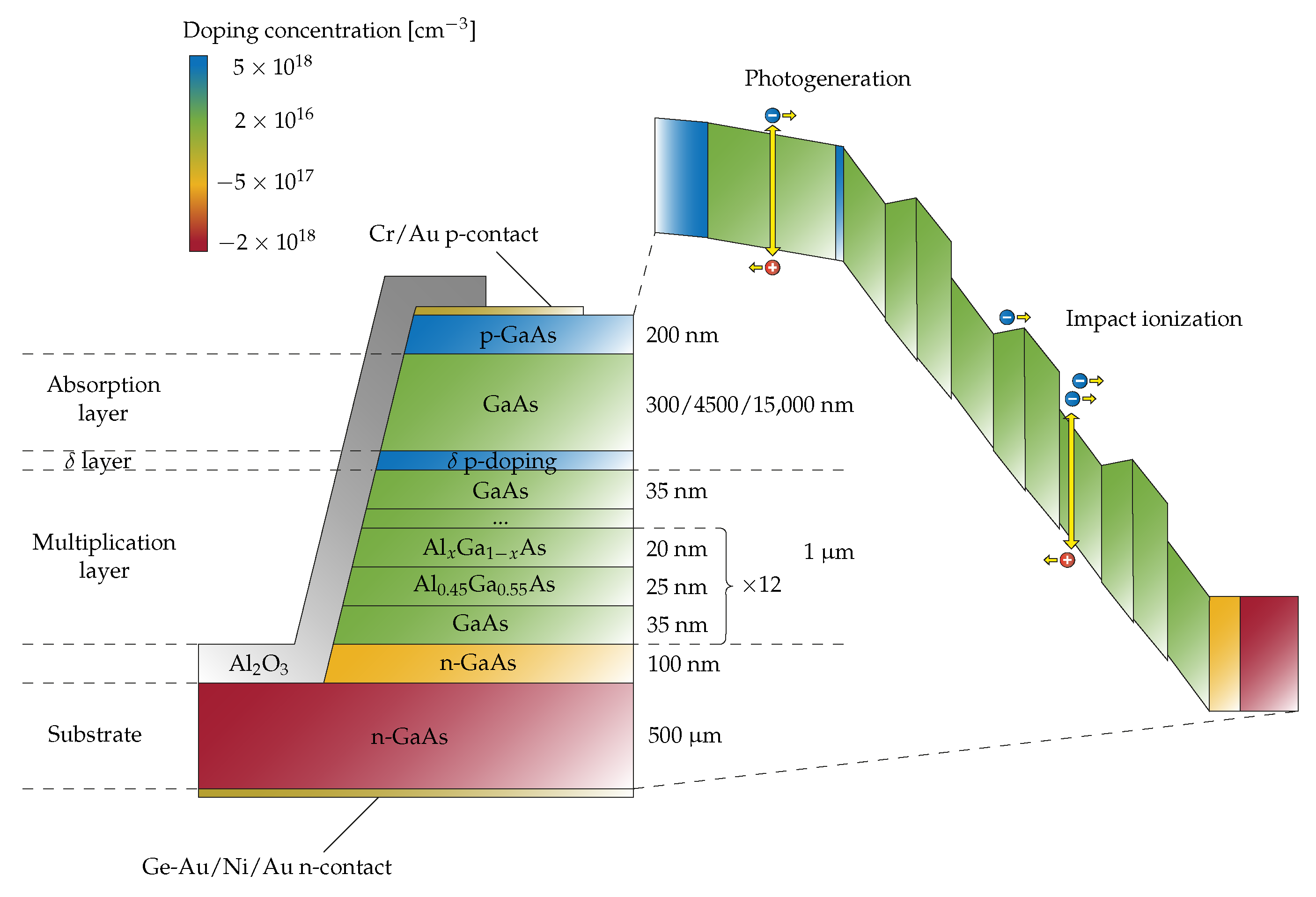
2.1. Devices Structure and Mode of Operation
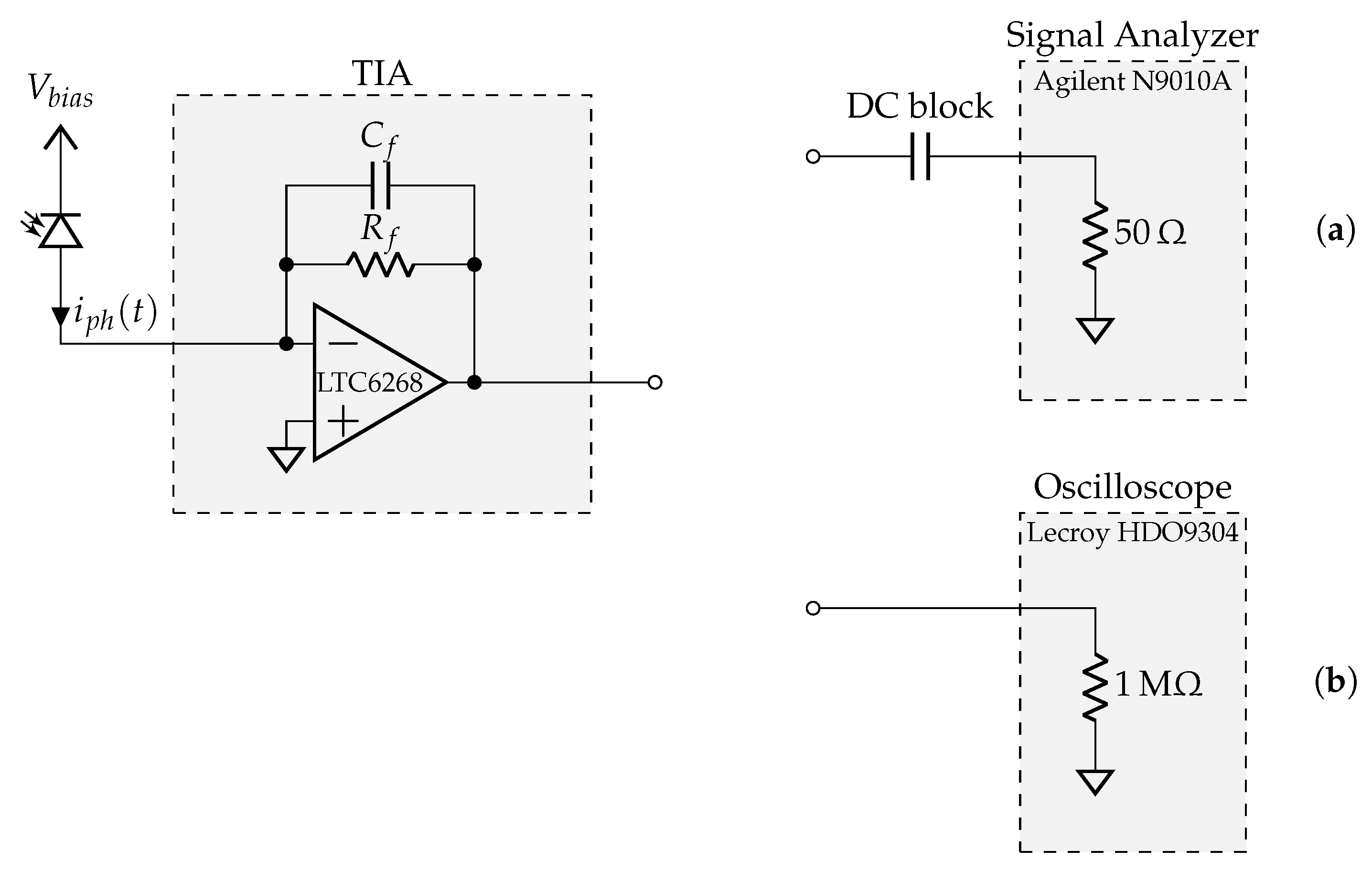
2.2. Experimental Setup
2.2.1. Measurements under Dark Conditions
2.2.2. Measurements under Light Conditions
3. Results
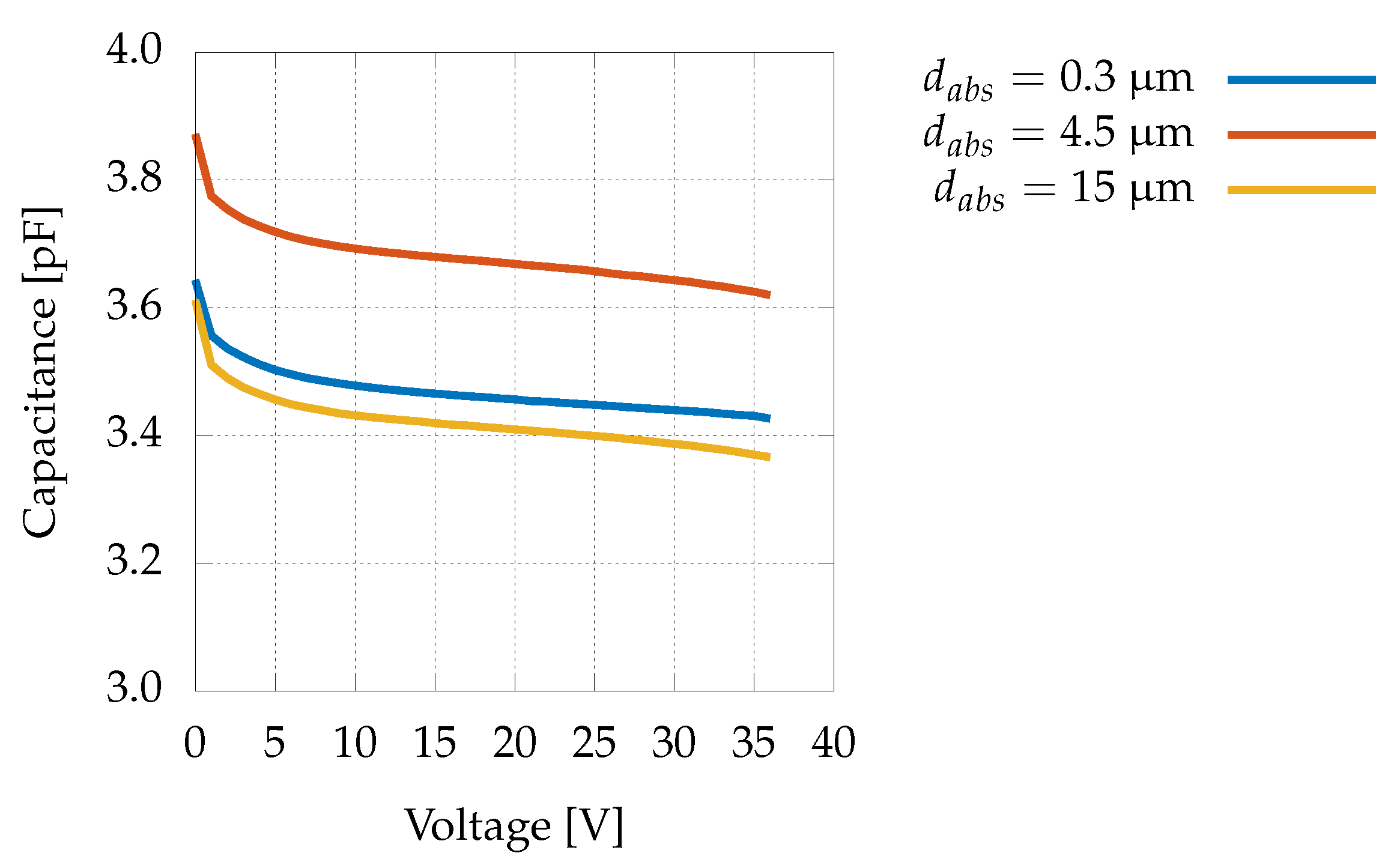
3.1. Capacitance
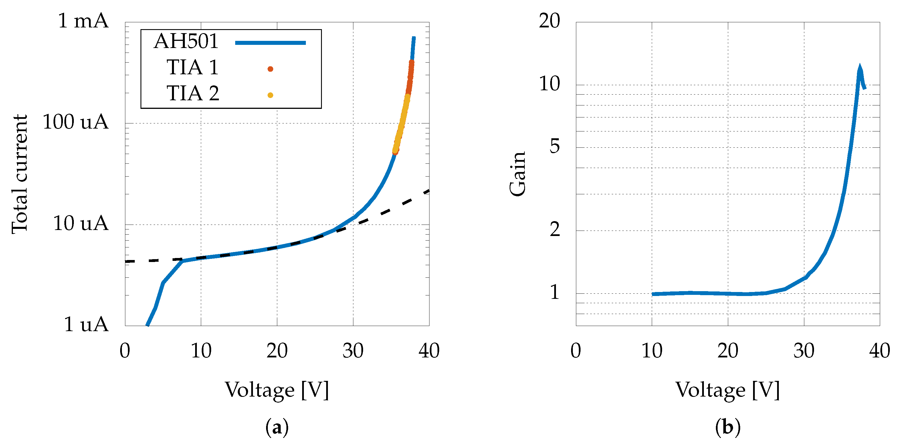
3.2. Gain
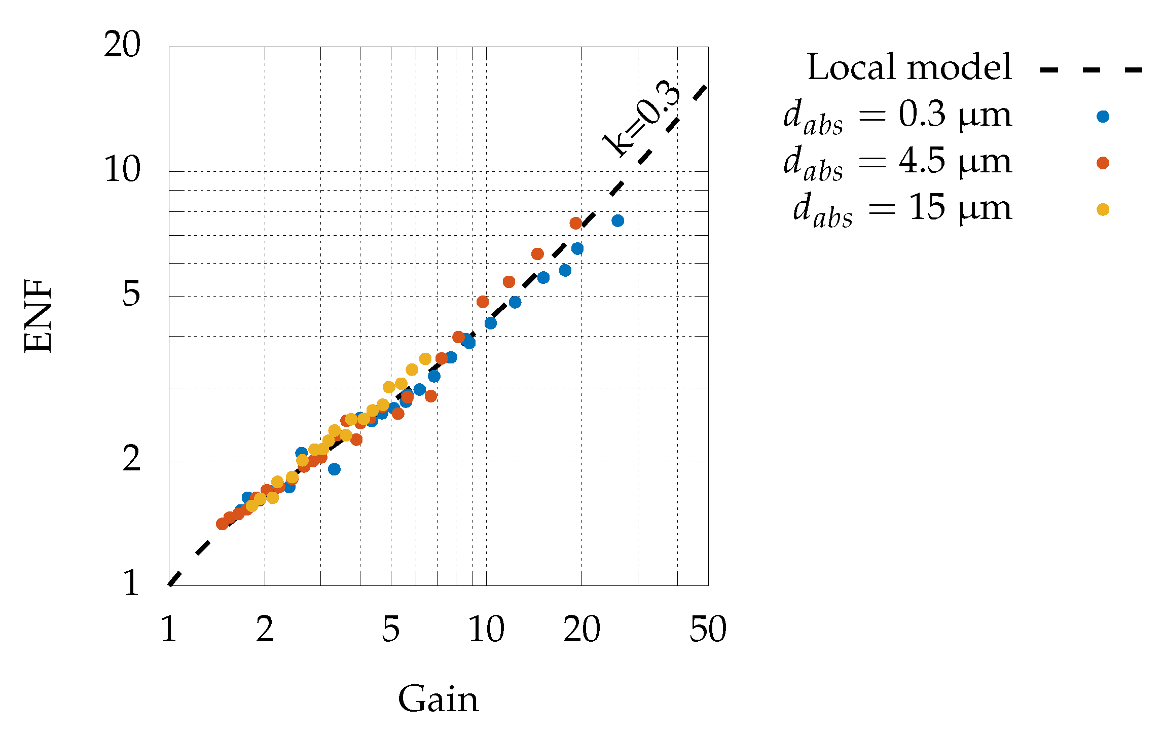
3.3. Excess Noise Factor
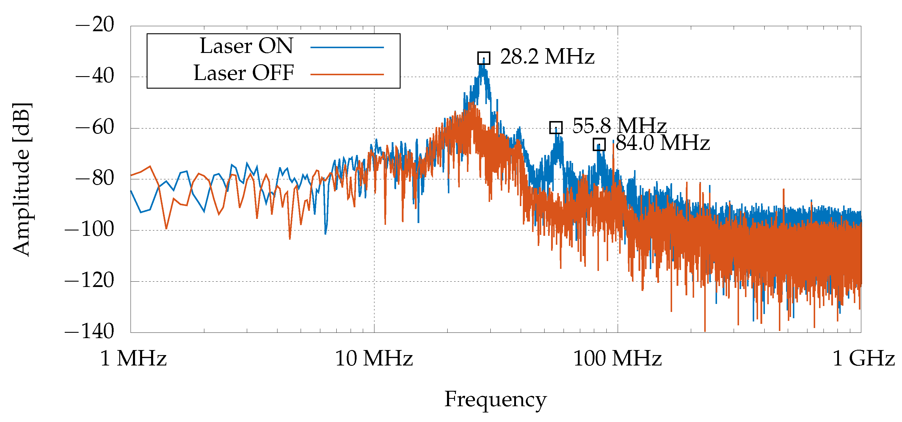
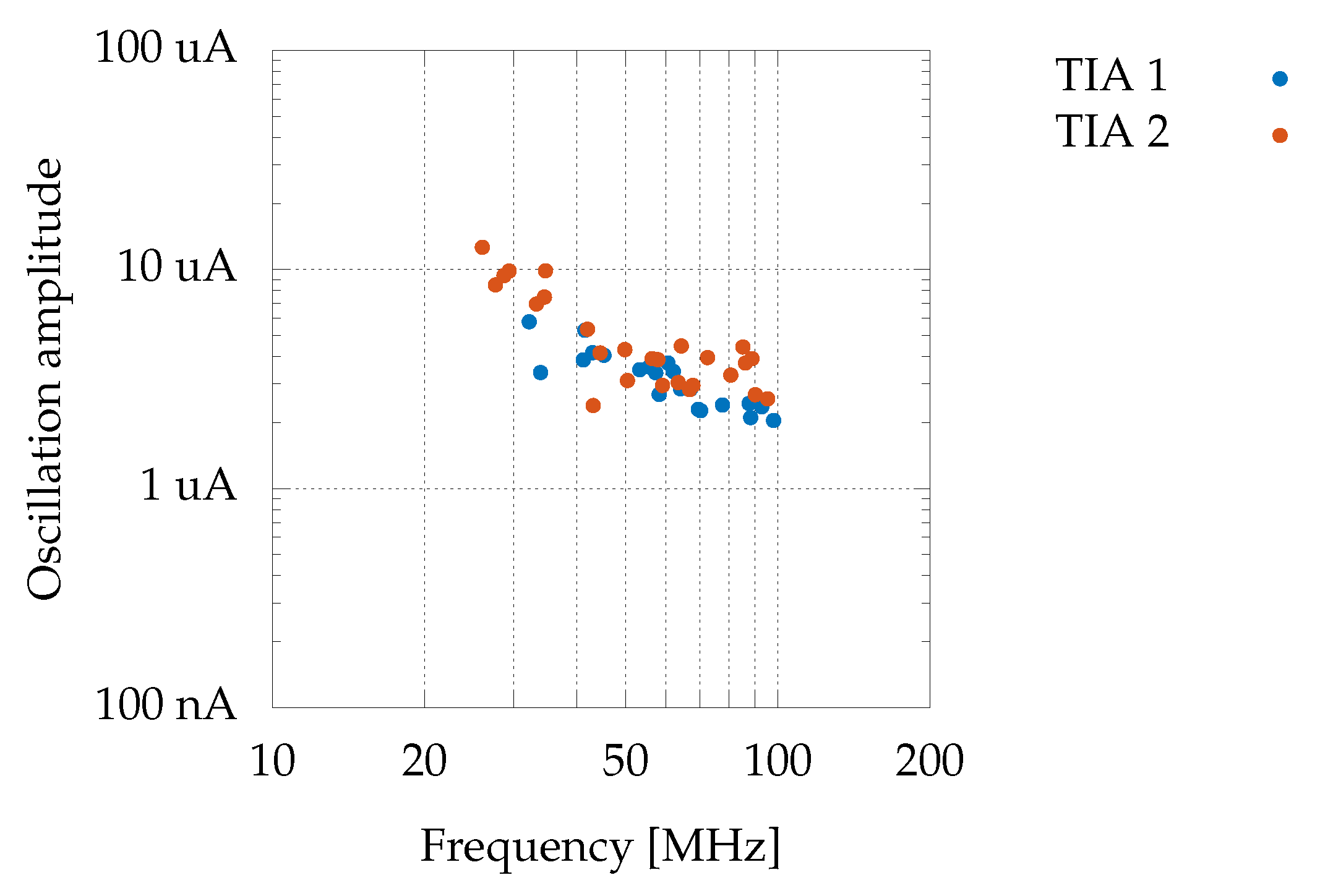
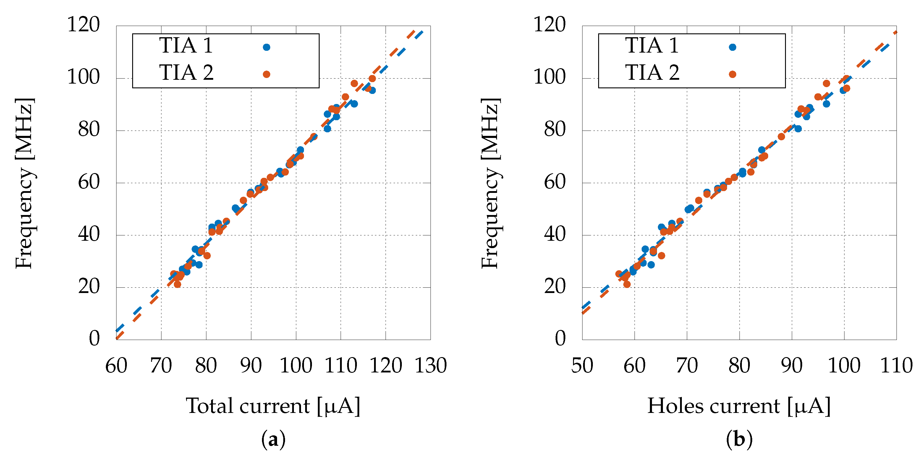
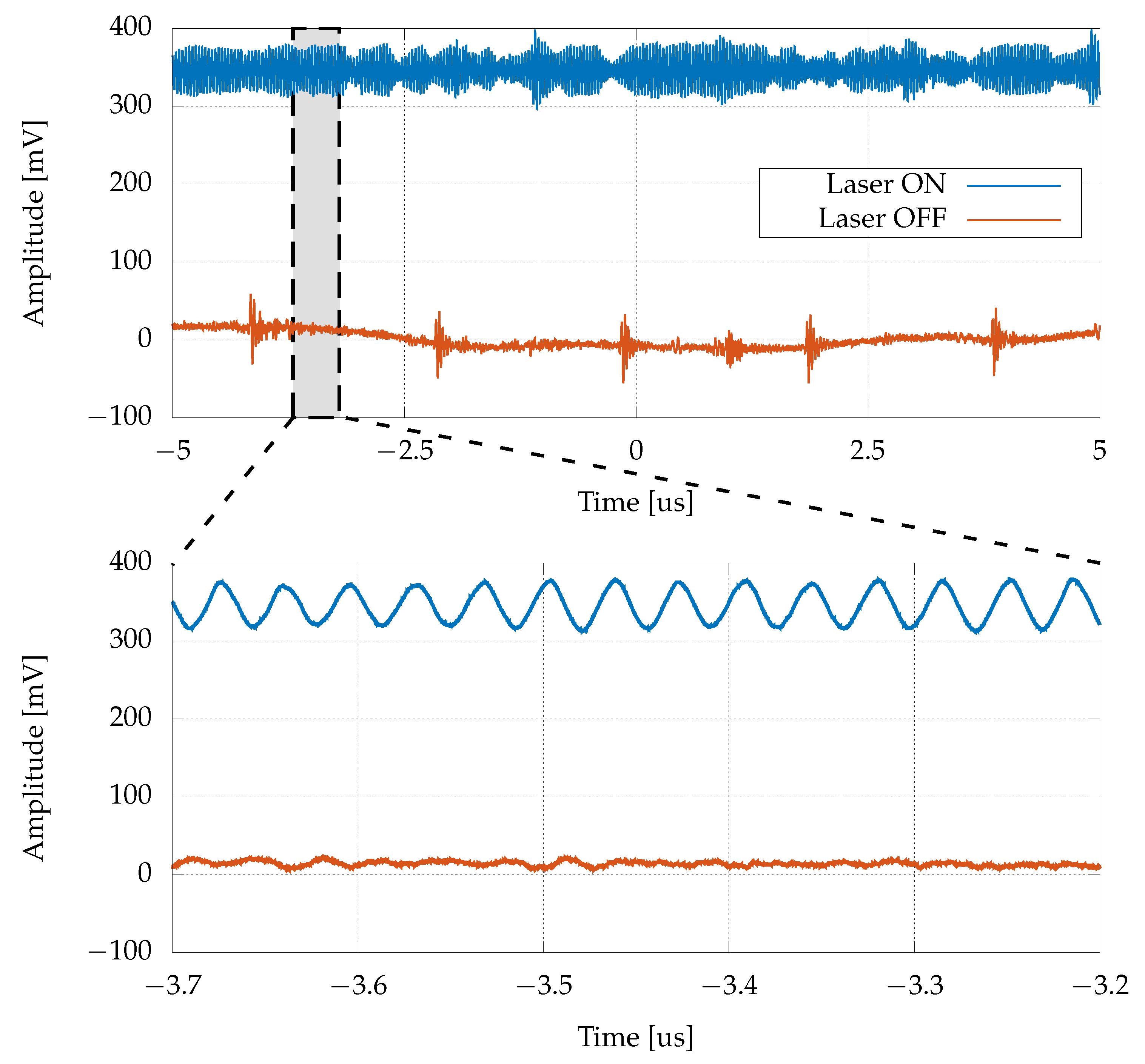
3.4. Oscillations at Fixed Laser Power
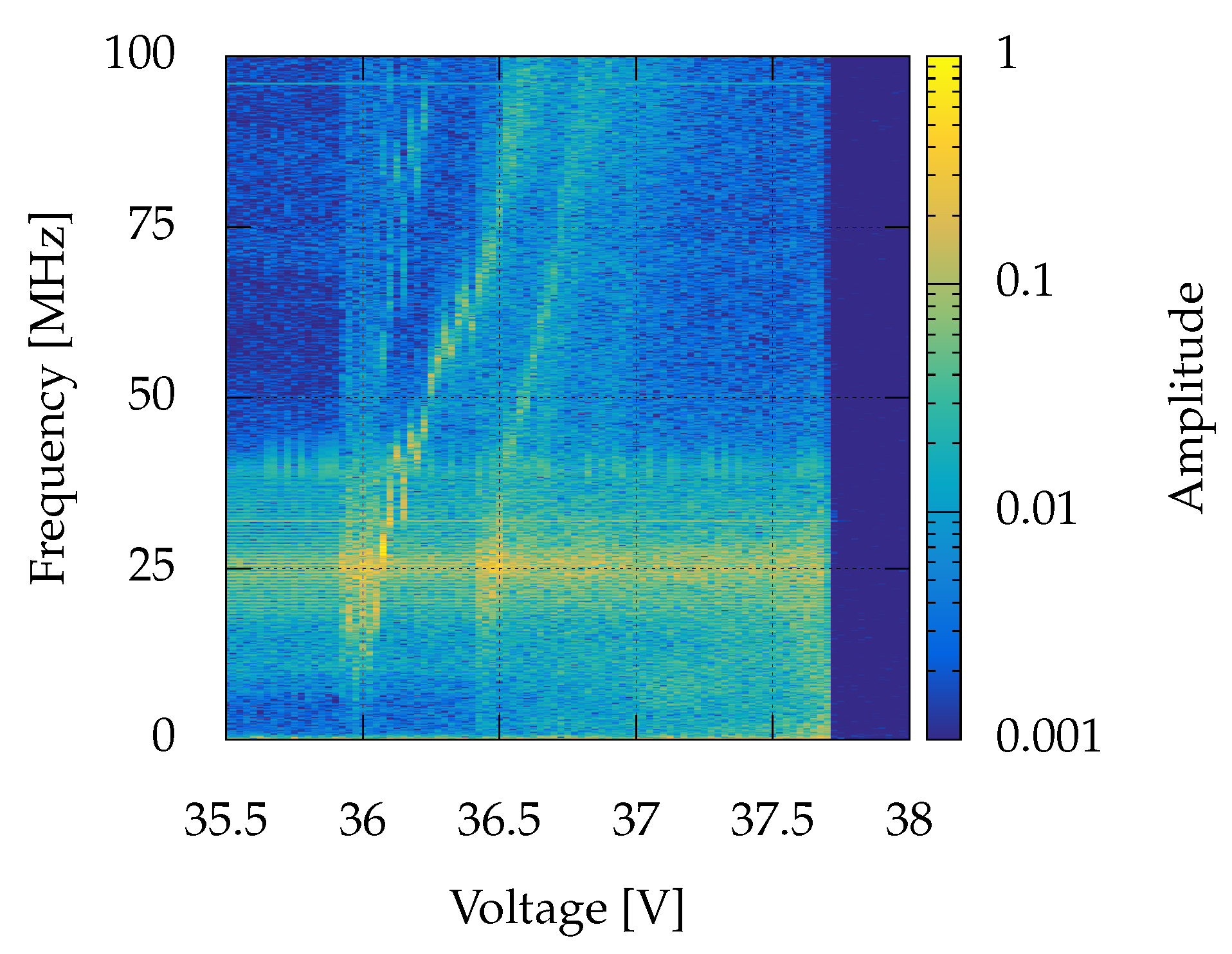
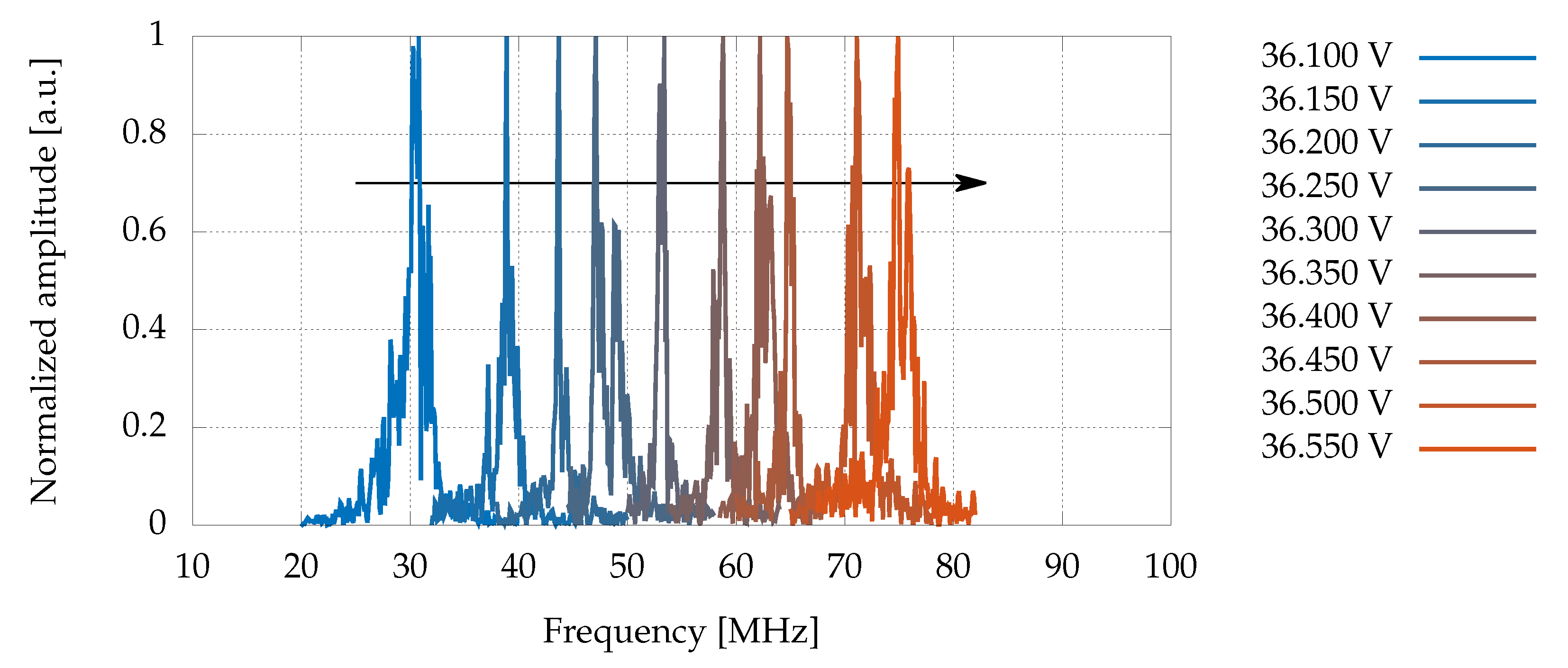
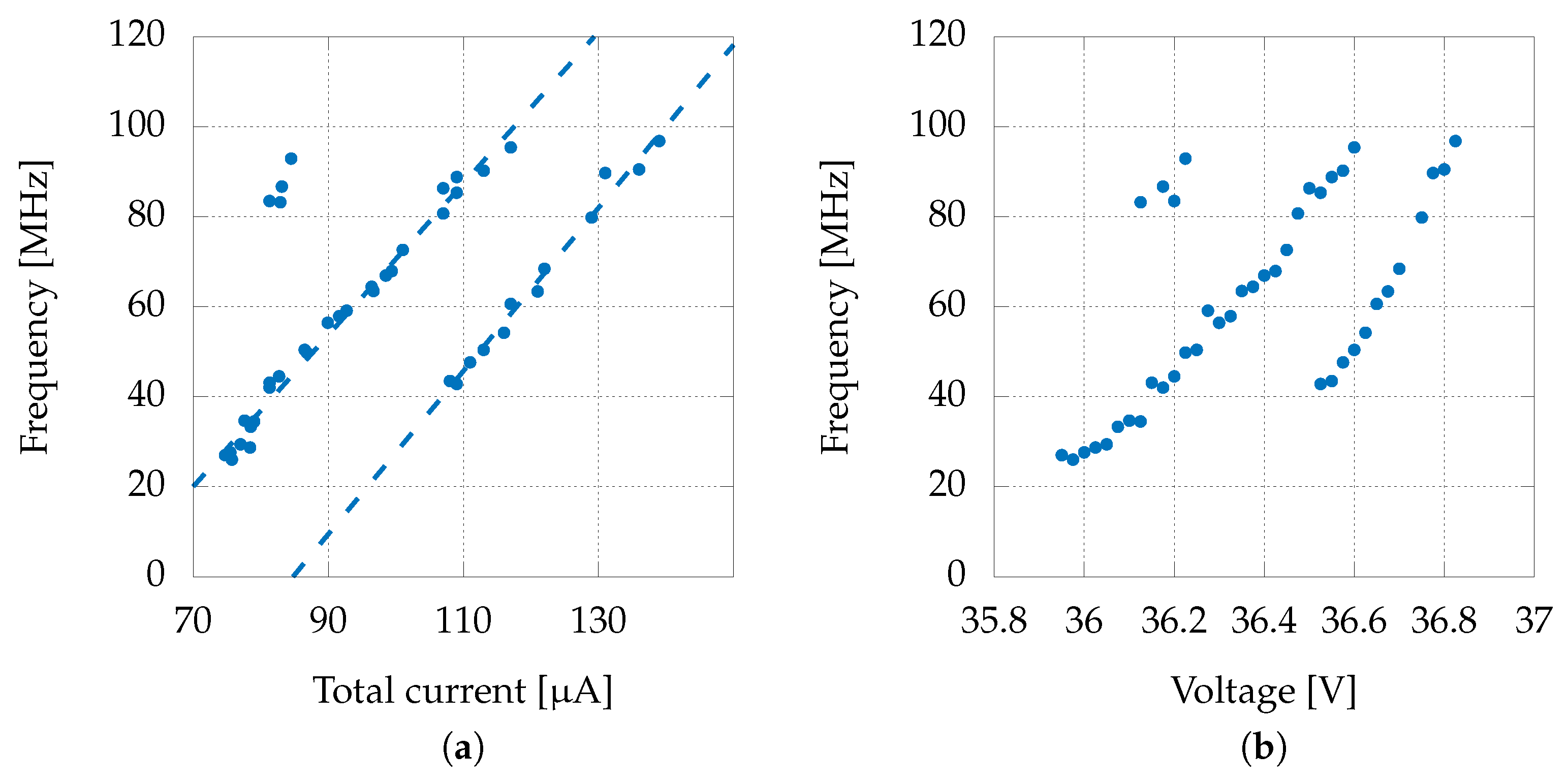
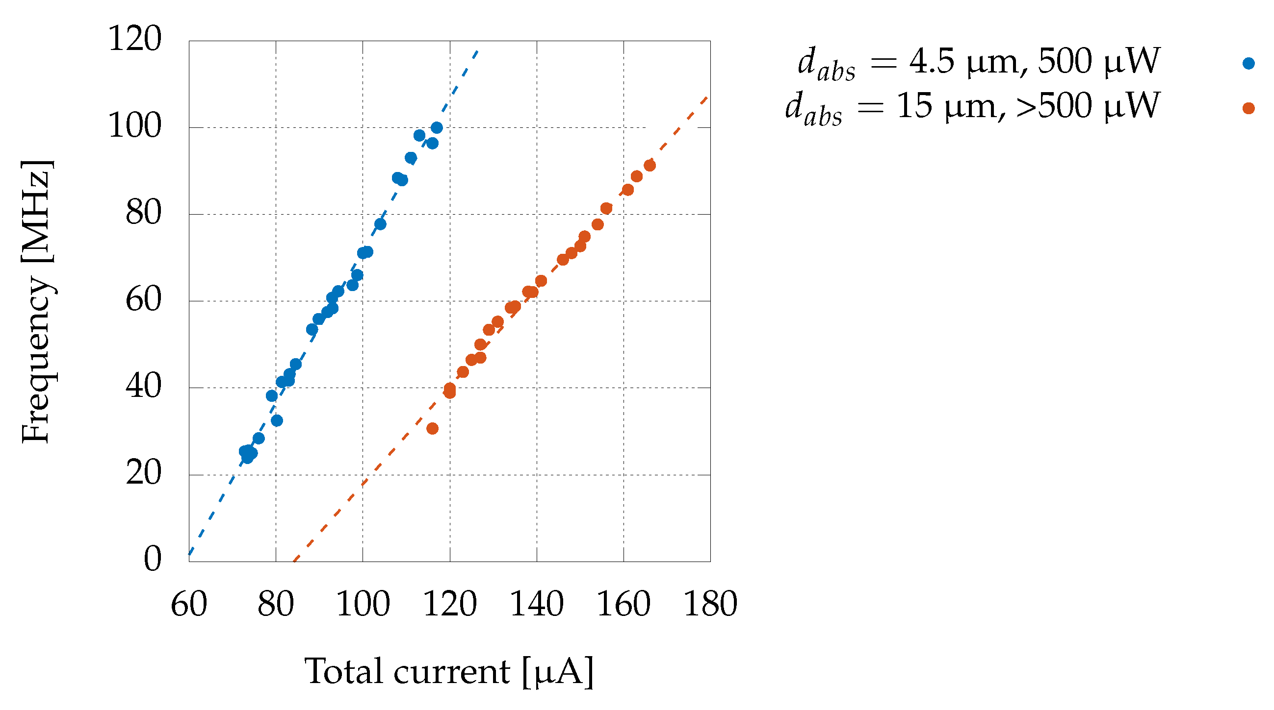
3.5. Oscillations at Fixed Bias
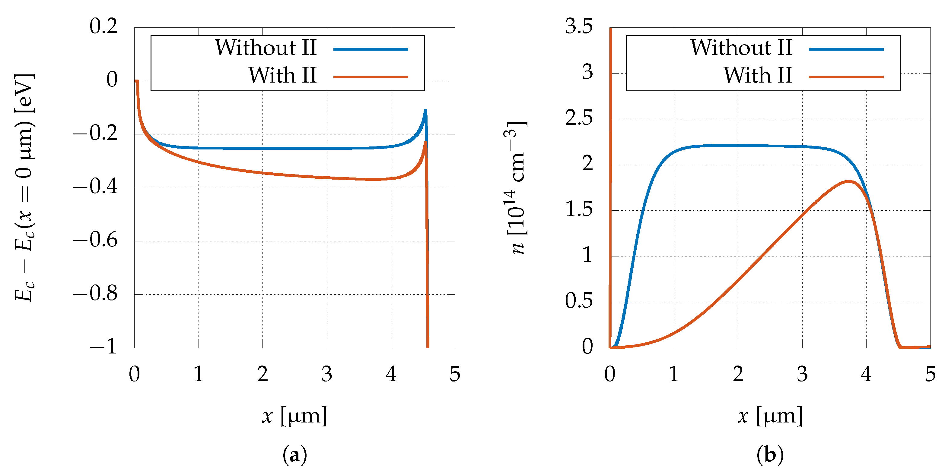
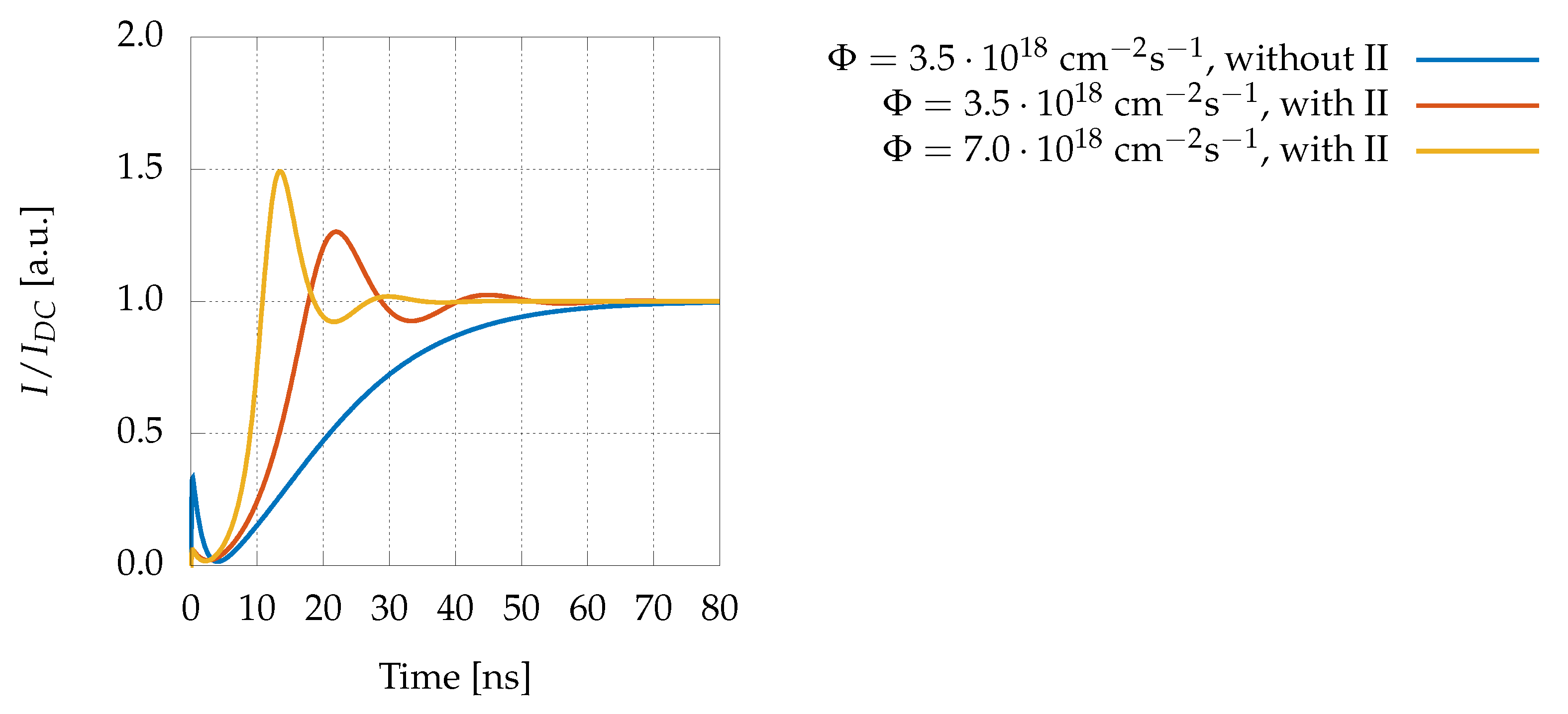
4. Discussion
Author Contributions
Funding
Institutional Review Board Statement
Informed Consent Statement
Data Availability Statement
Acknowledgments
Conflicts of Interest
Abbreviations
| APD | Avalanche Photodiode |
| GaAs | Gallium Arsenide |
| ENF | Excess Noise Factor |
| II | Impact Ionization |
| SAM | Separate Absorption and Multiplication region |
| PSD | Power Spectral Density |
| TIA | Transimpedance Amplifier |
References
- Taguchi, K.; Iwanczyk, J.S. Vision 20/20: Single Photon Counting X-Ray Detectors in Medical Imaging. Med. Phys. 2013, 40, 100901. [Google Scholar] [CrossRef] [PubMed]
- Jaszczak, R.J.; Coleman, R.E.; Lim, C.B. SPECT: Single Photon Emission Computed Tomography. IEEE Trans. Nucl. Sci. 1980, 27, 1137–1153. [Google Scholar] [CrossRef]
- Yun, I. Photodiodes: From Fundamentals to Applications; InTech: Rijeka, Croatia, 2012. [Google Scholar]
- MacLeod, S.J.; See, A.M.; Keane, Z.K.; Scriven, P.; Micolich, A.P.; Aagesen, M.; Lindelof, P.E.; Hamilton, A.R. Radio-Frequency Reflectometry on an Undoped AlGaAs/GaAs Single Electron Transistor. Appl. Phys. Lett. 2014, 104, 012114. [Google Scholar] [CrossRef]
- Teich, M.; Matsuo, K.; Saleh, B. Excess Noise Factors for Conventional and Superlattice Avalanche Photodiodes and Photomultiplier Tubes. IEEE J. Quantum Electron. 1986, 22, 1184–1193. [Google Scholar] [CrossRef]
- Nichetti, C.; Steinhartova, T.; Antonelli, M.; Biasiol, G.; Cautero, G.; Angelis, D.D.; Pilotto, A.; Driussi, F.; Palestri, P.; Selmi, L.; et al. Effects of p Doping on GaAs/AlGaAs SAM-APDs for X-rays Detection. J. Instrum. 2020, 15, C02013. [Google Scholar] [CrossRef]
- Williams, G.M.; Compton, M.; Ramirez, D.A.; Hayat, M.M.; Huntington, A.S. Multi-Gain-Stage InGaAs Avalanche Photodiode With Enhanced Gain and Reduced Excess Noise. IEEE J. Electron Devices Soc. 2013, 1, 54–65. [Google Scholar] [CrossRef]
- Pilotto, A.; Nichetti, C.; Palestri, P.; Selmi, L.; Antonelli, M.; Arfelli, F.; Biasiol, G.; Cautero, G.; Driussi, F.; Esseni, D.; et al. Optimization of GaAs/AlGaAs Staircase Avalanche Photodiodes Accounting for Both Electron and Hole Impact Ionization. Solid-State Electron. 2020, 168, 107728. [Google Scholar] [CrossRef]
- Maeda, M.; Minai, Y.; Tanaka, M. Photoinduced Anomalous Oscillations in Reach-through Avalanche Photodiodes. J. Appl. Phys. 2008, 48, 5324–5327. [Google Scholar] [CrossRef]
- Colja, M.; Cautero, M.; Menk, R.H.; Palestri, P.; Gianoncelli, A.; Antonelli, M.; Biasiol, G.; Dal Zilio, S.; Steinhartova, T.; Nichetti, C.; et al. Synchrotron Radiation Study of Gain, Noise, and Collection Efficiency of GaAs SAM-APDs with Staircase Structure. Sensors 2022, 22, 4598. [Google Scholar] [CrossRef] [PubMed]
- Steinhartova, T.; Nichetti, C.; Antonelli, M.; Cautero, G.; Menk, R.H.; Pilotto, A.; Driussi, F.; Palestri, P.; Selmi, L.; Koshmak, K.; et al. Influence of $\delta$ P-Doping on the Behaviour of GaAs/AlGaAs SAM-APDs for Synchrotron Radiation. J. Instrum. 2017, 12, C11017. [Google Scholar] [CrossRef]
- Alibava Systems Instruments for Detection. Picoammeter AH501B. Available online: https://alibavasystems.com/producto/picoammeter/ (accessed on 20 June 2023).
- Wulles, C.; Rafhay, Q.; Desrues, T.; Kaminski, A.; Theodorou, C. Parasitic Oscillation in the Low-Frequency Noise Characterization of Solar Cells. Solid-State Electron. 2022, 194, 108327. [Google Scholar] [CrossRef]
- McIntyre, R. Multiplication Noise in Uniform Avalanche Diodes. IEEE Trans. Electron Devices 1966, ED-13, 164–168. [Google Scholar] [CrossRef]
- Synopsys Inc. Sentaurus™ Device User Guide (Version L-2016.03); Technical report; Synopsys Inc.: Mountain View, CA, USA, 2013. [Google Scholar]
- Schöll, E. Nonlinear Spatio-Temporal Dynamics and Chaos in Semiconductors; Cambridge University Press: Cambridge, UK, 2001. [Google Scholar]


| TIA | |||
|---|---|---|---|
| 1.0 k | 15 nF | 11 kHz | |
| AH501B 1 | 1.0 M | 15 pF | 11 kHz |
| 1.0 G | <0.5 pF | ≈1 kHz | |
| Custom-made TIA 1 | 5.6 k | 2.5 pF | 11 MHz |
| Custom-made TIA 2 | 12 k | 4.5 pF | 2.9 MHz |
Disclaimer/Publisher’s Note: The statements, opinions and data contained in all publications are solely those of the individual author(s) and contributor(s) and not of MDPI and/or the editor(s). MDPI and/or the editor(s) disclaim responsibility for any injury to people or property resulting from any ideas, methods, instructions or products referred to in the content. |
© 2023 by the authors. Licensee MDPI, Basel, Switzerland. This article is an open access article distributed under the terms and conditions of the Creative Commons Attribution (CC BY) license (https://creativecommons.org/licenses/by/4.0/).
Share and Cite
Colja, M.; Cautero, M.; Arfelli, F.; Bertolo, M.; Biasiol, G.; Dal Zilio, S.; Driussi, F.; Menk, R.H.; Modesti, S.; Palestri, P.; et al. Experimental Characterization of Separate Absorption–Multiplication GaAs Staircase Avalanche Photodiodes under Continuous Laser Light Reveals Periodic Oscillations at High Gains. Photonics 2023, 10, 933. https://doi.org/10.3390/photonics10080933
Colja M, Cautero M, Arfelli F, Bertolo M, Biasiol G, Dal Zilio S, Driussi F, Menk RH, Modesti S, Palestri P, et al. Experimental Characterization of Separate Absorption–Multiplication GaAs Staircase Avalanche Photodiodes under Continuous Laser Light Reveals Periodic Oscillations at High Gains. Photonics. 2023; 10(8):933. https://doi.org/10.3390/photonics10080933
Chicago/Turabian StyleColja, Matija, Marco Cautero, Fulvia Arfelli, Michele Bertolo, Giorgio Biasiol, Simone Dal Zilio, Francesco Driussi, Ralf Hendrik Menk, Silvio Modesti, Pierpaolo Palestri, and et al. 2023. "Experimental Characterization of Separate Absorption–Multiplication GaAs Staircase Avalanche Photodiodes under Continuous Laser Light Reveals Periodic Oscillations at High Gains" Photonics 10, no. 8: 933. https://doi.org/10.3390/photonics10080933
APA StyleColja, M., Cautero, M., Arfelli, F., Bertolo, M., Biasiol, G., Dal Zilio, S., Driussi, F., Menk, R. H., Modesti, S., Palestri, P., Pilotto, A., & Cautero, G. (2023). Experimental Characterization of Separate Absorption–Multiplication GaAs Staircase Avalanche Photodiodes under Continuous Laser Light Reveals Periodic Oscillations at High Gains. Photonics, 10(8), 933. https://doi.org/10.3390/photonics10080933