Abstract
Plasmonic structures based on stacked layers of metal and dielectric materials excel as broadband absorbers because of the nonlinear relationship between the compound materials’ dispersion characteristics and the multilayered structure’s actual performance. In this work, radiation absorption along the plasmonic absorber is studied. Broadband absorptance spectra play an important role in applications such as photovoltaics, detectors, modulators, and emitters. We propose and analyze plasmonic stacked structures that exhibit high broadband absorption. For this purpose, an inverse design approach has been implemented using a conventional genetic algorithm as a global optimizer in conjunction with a pattern search as a local optimizer. The proposed strategy found structures with absorption covering the visible spectrum, maintaining its performance for high incident angles.
1. Introduction
Broadband absorbers with wide-angle operations are intensively studied for their importance in a myriad of applications. They generally are obtained using noble metals to enhance light absorption by exploring plasmon excitation [1,2,3,4], thus allowing maximum energy utilization. The resonant nature of plasmons can impose a restriction on the bandwidth of absorption, and one way to overcome this limitation is the use of complex designs such as metamaterial absorbers [3] or nanoparticles [4], resulting in structures that require complex fabrication processes or have low fabrication error tolerance [4].
In this work, we investigate absorption using multiple metallic and dielectric stacked films, which, in principle, can provide broadband absorption without requiring complex designs based on resonator disks, cubes, or pyramids, thus allowing low fabrication complexity for large-area absorbers. The changes in the light spectrum caused by the phase shift of transmitted electromagnetic fields in metallic-dielectric interfaces can be engineered in a proper way by using combinations of a set of interfaces. This phenomenon has been widely studied, and it has been demonstrated by several structures for solar energy harvesting and color filtering applications [5,6,7,8,9,10,11,12,13].
Arrays of silicon carbide micro pyramids have also exhibited absorption with respect to the direction of propagation in the infrared regime [14]. This singular property finds application in one-way infrared sources and passivecooling systems. Furthermore, most of the broadband absorbers with high absorption are based on metamaterials, which require surface patterning features, including gratings, typically fabricated by complex and costly nanofabrication techniques such as electronbeam lithography. Consequently, they exhibit economical and scalable limitations [15]. Additionally, the absorption mechanism in metamaterial-based absorbers depends on the electric and magnetic resonances produced by resonators with complex geometries, resulting in a limited absorption bandwidth. To increase broadband absorption, several resonators with different resonant frequencies can be combined [15,16], and the complexity of their fabrication processes increases as the number of resonators increases. On the other hand, we considered Fabry–Perot-based cavities absorbers, composed of metal–insulator–metal (MIM) layers that can be used for this purpose, and they can be easily fabricated in large areas by deposition of the materials without patterning micro/nano structures.
In this work, we propose a novel stacked metallic-dielectric layered structure and optimize it using a genetic algorithm (GA) in conjunction with a pattern search (PS), resulting in a broadband absorbance for the visible spectrum. The analyzed multilayer stack is an exciting example to demonstrate the proposed inverse design algorithm’s effectiveness because it is a multi-objective problem with several variables, such as wavelengths, materials, layer thickness, incident angles, and polarization. The usefulness of inverse design techniques for discovering nanophotonic devices for novel applications in situations where the traditional intuition-based procedures fail has been demonstrated in [17,18,19,20].
Here, the geometrical parameters of the thin layers have been optimized to obtain high absorption over a broadband interval of frequencies. The results show that the absorption can be arbitrarily engineered for incident light allowing light manipulation with applications for detection and sensing.
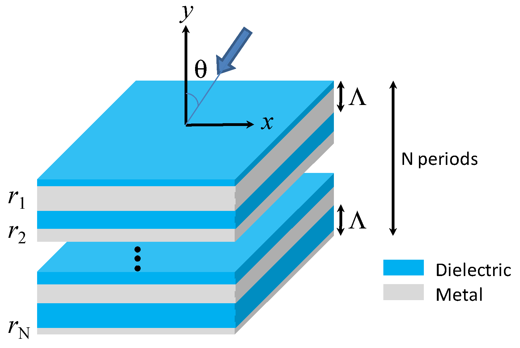
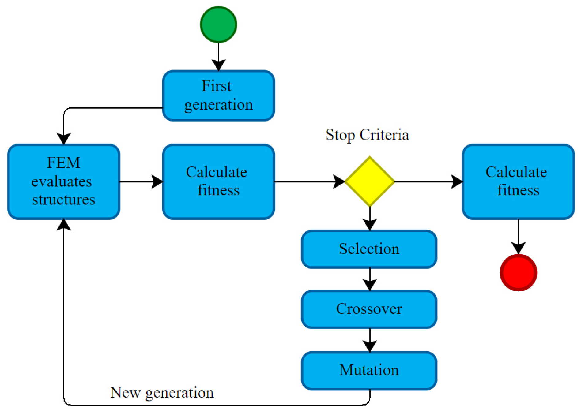
2. Design of the Absorbers
We considered the search space determined by an array of ten different bi-layer cells. Each cell comprises a layer of silica and a layer of metal (nickel, gold, or silver), with a fixed period of 100nm. The fraction of metal (ri) in each cell is a real number parameter to be determined by the implemented search algorithm. In this scenario of such an infinite search space, the chosen optimization method is a suitable technique since it is indifferent to the initial guess. GA is well known for its good performance in multidimensional domains as a global optimizer in electromagnetic design problems [21,22,23,24,25,26].
Resonant cavities of the Fabry–Perot (FP) type composed of metal–dielectric–metal (MDM) have been widely studied. These structures were used to design narrowband absorbers [26,27,28] and tunable optical filters [29,30]. For the development of these resonant structures, it is necessary that the strict condition n = κ is obeyed, where n is the refractive index of the dielectric and κ is the metal extinction coefficient. In our work, the goal is to design multiple resonant cavities to develop a broadband absorber. The schematic of the proposed absorber is shown in Figure 1. The optimization tools are used to find the ideal thicknesses for maximum absorption.
Figure 1.
Schematic of the absorber, which has one tunable parameter (ri). An entire structure is composed of 10 such planar cells.
The dielectric and metal refractive indexes were taken from [29,30], respectively. The penetration depth of the electric field in the metal (δ) can be calculated as the inverse of the propagation constant (k). Using SPP dispersion ratio solutions on a dielectric metal interface, the value of δ can be calculated as [31,32],
where λ is the free-space wavelength of the incident light, εm and εd are the absolute value of permittivity for the metallic and dielectric layers, respectively. The εm module was calculated using the relations:
The behavior of the penetration depth of the field in the visible spectrum for the three metals is shown in Figure 2. In all cases, the penetration depth decreases when the wavelength increases. Silver and gold exhibit greater penetration depth than nickel in the analyzed frequency spectrum.
Figure 2.
Penetration depth (δ) of the used metals.
The absorptance spectrum for each structure was obtained by numerical analysis through a finiteelement method (FEM) approach using the commercial software COMSOL Multiphysics [9,27]. The simulation software receives the geometric and material parameters and returns the absorption, which feeds the GA loop. The average of the absorption has been optimized considering normal incidence (θ = 0), and its value is obtained by
The flowchart of the simulation and the interaction between COMSOL and the GA algorithm is shown in Figure 3.
Figure 3.
GA’s workflow.
As with any other GA algorithm, each iteration involves selecting parents to generate the offspring, which would become the individuals for the next generation. For this purpose, we used the roulette wheel selection. It means that the highestscoring individuals (higher fitness) have more chances of being selected for reproduction. The two selected parents’ genes were combined for each new individual in a single uniformly distributed random point crossover.
The probability of crossover is defined as the probability that crossover will occur; if it does not, the new individual is an identical copy of one of the parents. Each gene of each new individual is then subjected to a probability of mutation, where that given gene is changed randomly in the full range of possible states for that particular position. After the new generation is created, these individuals are simulated and have their fitness evaluated. They are then ranked with the previous generation. The best individuals of this rank are kept for parenting in the next generation.
Since we considered a large number of individuals (50) per generation to increase the probability of obtaining a good number of possible candidates with a high absorption during the optimization process, we adopted the following stop criteria: maximum number of generations = 100 or number of generations without changes in the average absorption = 15. Figure 4 shows the evolution of the average absorption of the best individual as a function of the number of generations when assuming Ag as metallic layers. For this particular case, the stop criterion was the number of generations without changes, and the optimization stopped at generation number 60. Similar behavior has been observed for the other two metals.
Figure 4.
Evolution of the average absorption as a function of the number of generations.
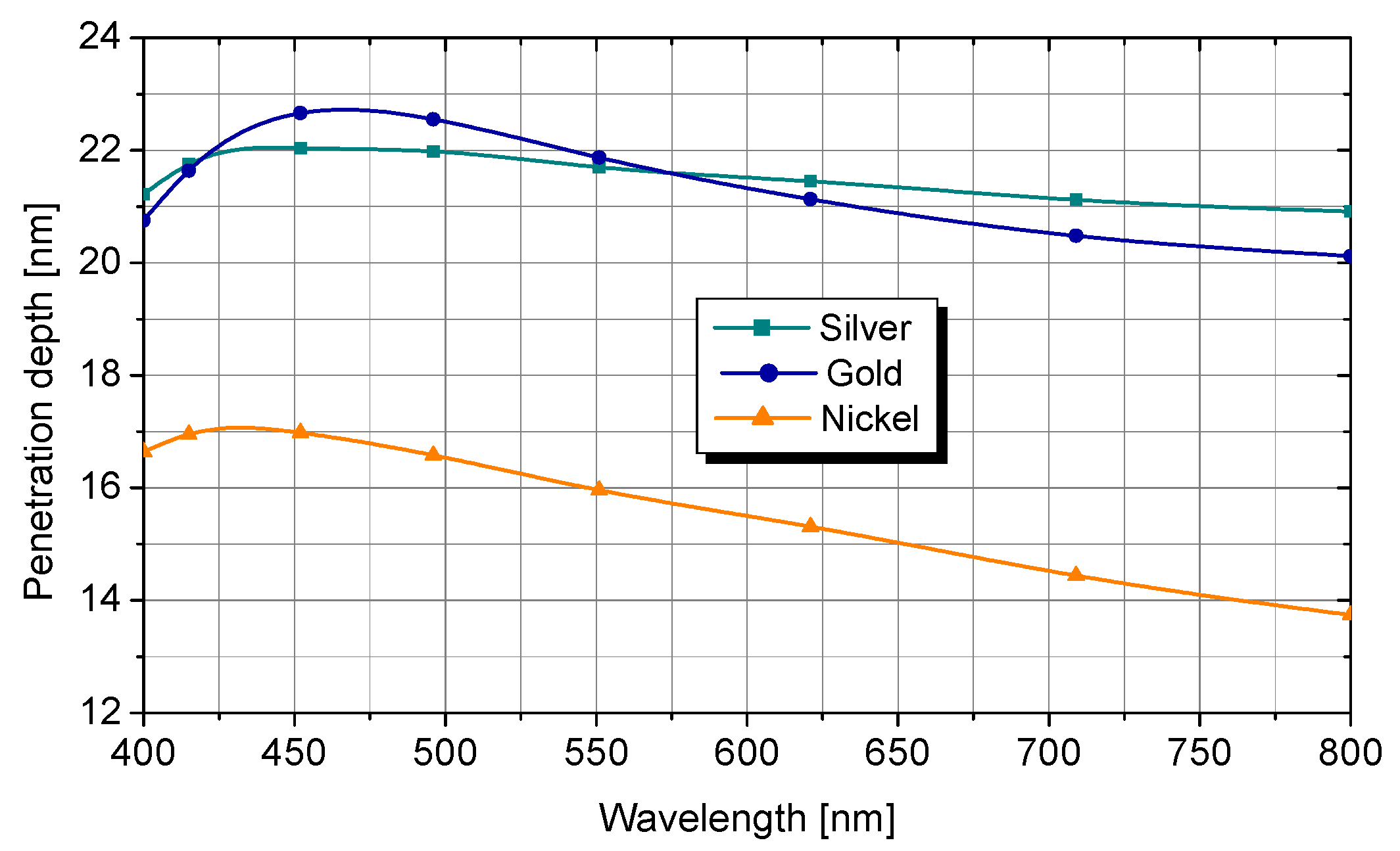
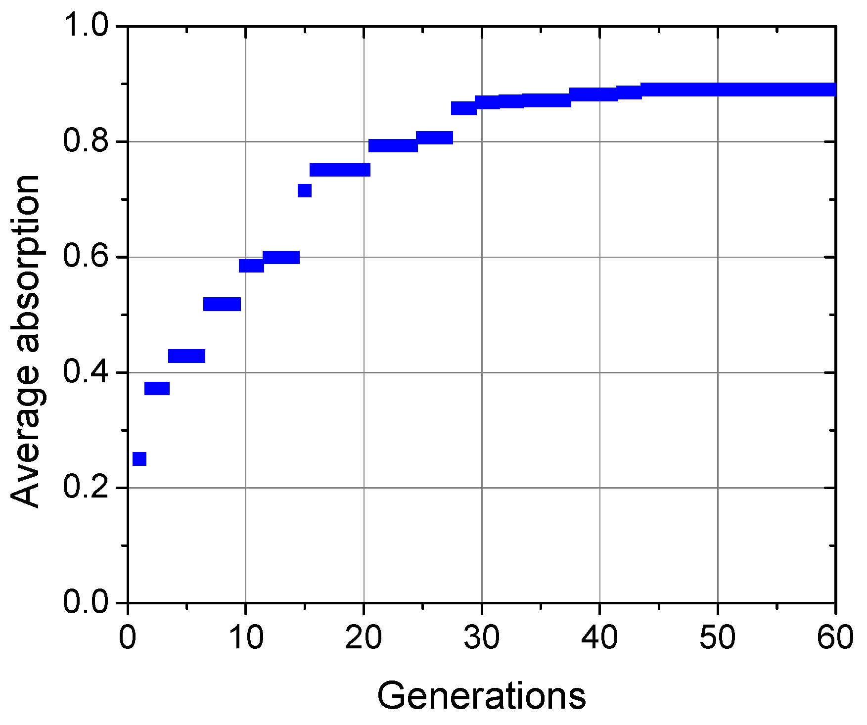
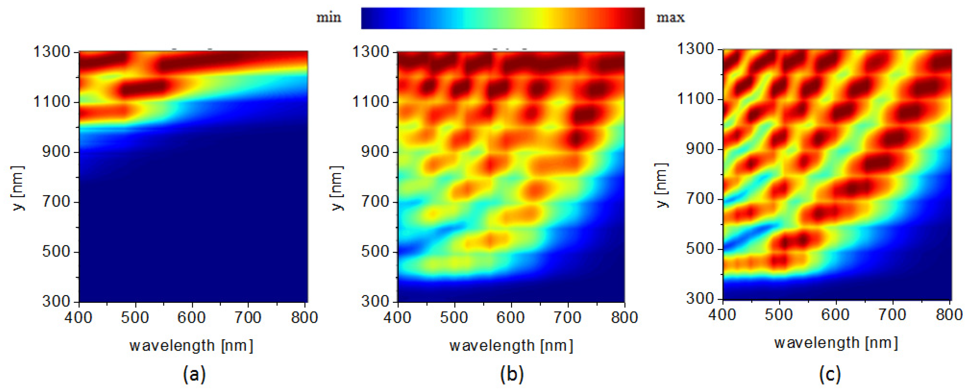
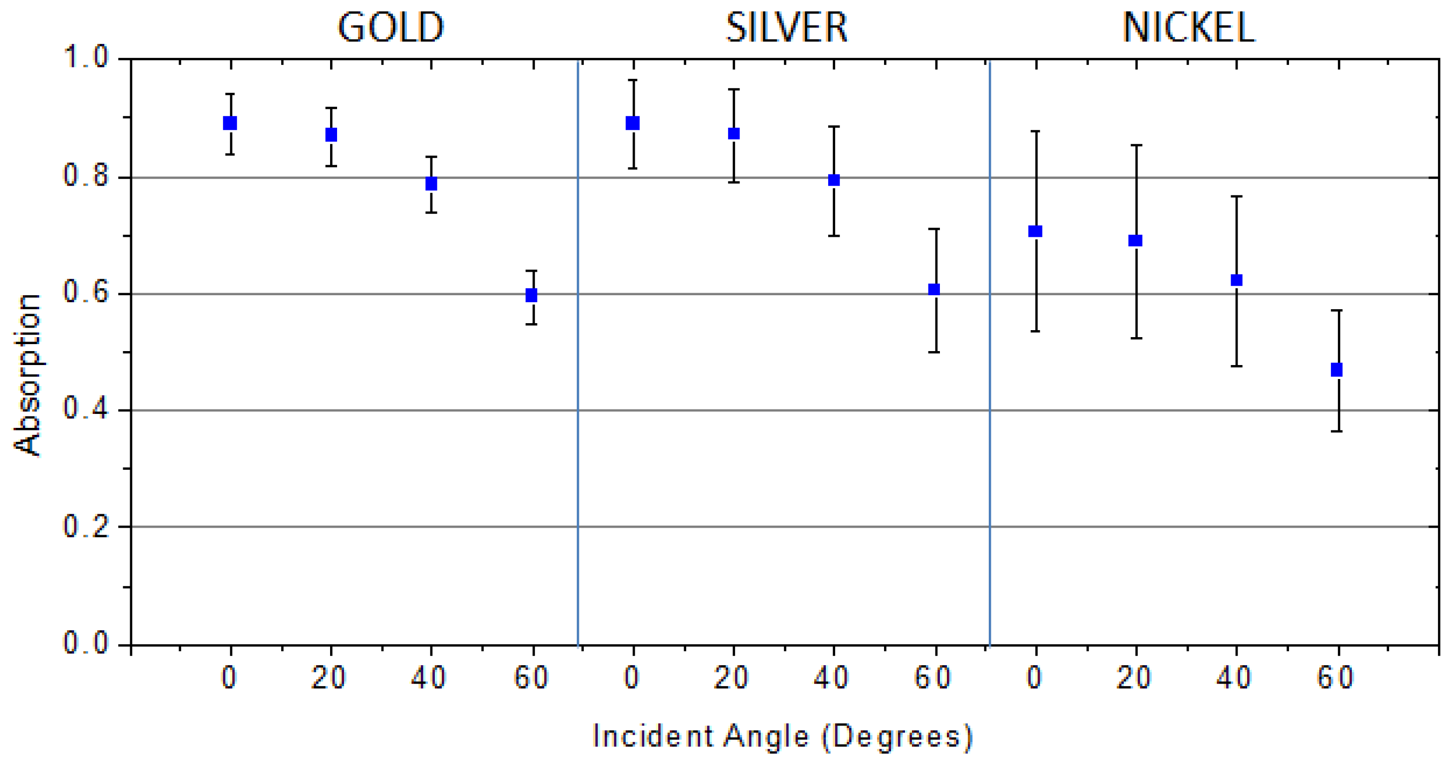
3. Results and Discussion
Figure 5 shows the absorption behavior of the structure composed of SiO2 and metal (Ni, Au, and Ag) for different angles of incidence, downwards, after optimization using GA.
Figure 5.
Absorbance spectra of the stacked layered structure using SiO2 and (a) nickel, (b) gold, and (c) silver. Insets show the proportion of materials distribution.
One can observe in Figure 5a left an absorption above 80% that decreases with the wavelength increasing up to half of the initial value to approximately 40%. Similar behaviors are seen in Figure 5b,c for Au and Ag, respectively. When we analyze the absorption, the structures exhibit the behavior of a broadband absorber with values above 80% in both cases.
It can also observe the normalized H-field distribution inside the optimized stack thicknesses for all the simulated wavelengths in Figure 6.
Figure 6.
Normalized H-field distribution inside the optimized multilayered stack as a function of the wavelength for downward incidence (a) nickel, (b) gold, and (c) silver.
According to Table 1, which shows the thickness of the metals in each pair, and Figure 7, it is possible to observe that for Ag and Au, the thicknesses of the metals are much smaller than the penetration depth, as seen in Figure 2. This fact explains the high absorption, in normal incidence, in the structures composed of Au or Ag; the field can penetrate all pairs except forpair number 10, as seen in Figure 6b and Figure 6c, respectively. For Ni (see Figure 6a), the field can only penetrate up to pair number 3; for all other pairs (4–10), the thickness of the metal is much greater than Ni’s penetration depth, and the field cannot be absorbed in these pairs.
Table 1.
Optimized values of metal thickness in each metal/SiO2.
Figure 7.
Metal thickness as a function of the stack layer position.
The average absorption values and the standard error deviation, as a function of the incident angle and metallic materials, are shown in Figure 8. Values of average absorption higher than 88% can be obtained.
Figure 8.
Average absorption and standard error deviation as a function of the incident angle and metallic materials.
The proposed absorbers in this work exhibit similar average values compared with previously published works [32,33,34,35,36] with the advantage of being a lithography-free fabrication process. In [32], a plasmonic metamaterial absorber composed of nanocomposite of gold and silica percolated over a flexible polymer film exhibited almost perfect absorption at visible frequencies, while in [33], a metamaterial composed of nanopillars of Ni over a Ni substrate attained 96% in the interval of 400nm to 760nm. In [34], an all metallic absorber was presented. It is composed of Au nanoparticles with 97% of absorption and covers the wavelength interval from 320nm to 650nm. In [35], a metasurface absorber on a flexible film was proposed using a simple fabrication process. It consists of a polyimide nanocone substrate coated with gold and tungsten layers, exhibiting over 96% optical absorption in the visible range. In [36], an absorber consisting of two layers of tungsten resonators on a silicon dioxide substrate coated with additional SiO2 materials exhibiting an average absorption of 92% from 400 nm to 2400 nm with stable oblique incident angles up to 45° was reported. All these absorbers need complex and expensive fabrication processes, which are unnecessary in the proposed stacked multilayer absorber.
4. Conclusions
In this work, we demonstrated how to obtain stacked layered metallic-dielectric structures that exhibit high absorption using an automated design based on a genetic algorithm. The proposed device was numerically analyzed by the FEM and demonstrated an average absorption above 88% for the visible band. The proposed lossy stack of materials can achieve near-unity absorption within a broadband interval of frequencies. The stacked thin films presented in this work are free from complex surface patterns and can be fabricated over large areas using conventional vapor deposition or electrochemical methods. The proposed broadband absorber could enhance the optical performance for applications of infrared thermal emitters, imaging and photodetectors, radiative cooling, and solar energy conversion.
Author Contributions
Conceptualization, D.F.R., I.L.G.d.S., and V.F.R.-E.; methodology, D.F.R., I.L.G.d.S., and V.F.R.-E.; software, D.F.R., I.L.G.d.S., and V.F.R.-E.; formal analysis, D.F.R., I.L.G.d.S., V.F.R.-E., and G.N.M.-S.; resources, D.F.R., I.L.G.d.S., V.F.R.-E., and G.N.M.-S.; writing—original draft preparation, D.F.R., I.L.G.d.S., and V.F.R.-E.; writing—review and editing, D.F.R., I.L.G.d.S., V.F.R.-E., and G.N.M.-S.; visualization, D.F.R., I.L.G.d.S., V.F.R.-E., and G.N.M.-S.; funding acquisition, D.F.R., I.L.G.d.S., V.F.R.-E., and G.N.M.-S. All authors have read and agreed to the published version of the manuscript.
Funding
This study was financed in part by the Coordenação de Aperfeiçoamento de Pessoal de Nível Superior—Brasil (CAPES)—Finance Code 001, CNPQ (Process: 309100/2018-6), FAPESP/MCTI/MC Process: 2015/24517-8, UFBA, ICTI-UFBA, IFBA, FAPESB (079/2016).
Institutional Review Board Statement
Not applicable.
Informed Consent Statement
Not applicable.
Data Availability Statement
Data will be made available on request.
Conflicts of Interest
The authors declare no conflict of interest. The funders had no role in the design of the study; in the collection, analyses, or interpretation of data; in the writing of the manuscript; or in the decision to publish the results.
References
- Watts, C.M.; Liu, X.; Padilla, W.J. Metamaterial Electromagnetic Wave Absorbers. Adv. Mater. 2012, 24, OP98–OP120. [Google Scholar] [CrossRef]
- Yu, P.; Besteiro, L.V.; Huang, Y.; Wu, J.; Lu, L.; Tan, H.H.; Jagadish, C.; Wiederrecht, G.P.; Govorov, A.O.; Wang, Z. Broadband Metamaterial Absorbers. Adv. Opt. Mater. 2019, 7, 1800995. [Google Scholar] [CrossRef]
- Ding, F.; Dai, J.; Chen, Y.; Zhu, J.; Jin, Y.; Bozhevolnyi, S.I. Broadband near-infrared metamaterial absorbers utilizing highly lossy metals. Sci. Rep. 2016, 6, 39445. [Google Scholar] [CrossRef] [PubMed]
- Hedayati, M.K.; Javaherirahim, M.; Mozooni, B.; Abdelaziz, R.; Tavassolizadeh, A.; Chakravadhanula, V.S.K.; Zaporojtchenko, V.; Strunkus, T.; Faupel, F.; Elbahri, M. Design of a Perfect Black Absorber at Visible Frequencies Using Plasmonic Metamaterials. Adv. Mater. 2011, 23, 5410–5414. [Google Scholar] [CrossRef] [PubMed]
- Sergeant, N.P.; Pincon, O.; Agrawal, M.; Peumans, P. Design of wide-angle solar-selective absorbers using aperiodic metal-dielectric stacks. Opt. Express 2009, 17, 22800–22812. [Google Scholar] [CrossRef] [PubMed]
- Wang, W.; Cui, Y.; He, Y.; Hao, Y.; Lin, Y.; Tian, X.; Ji, T.; He, S. Efficient multiband absorber based on one-dimensional periodic metal–dielectric photonic crystal with a reflective substrate. Opt. Lett. 2014, 39, 331–334. [Google Scholar] [CrossRef]
- Diem, M.; Koschny, T.; Soukoulis, C.M. Wide-angle perfect absorber/thermal emitter in the terahertz regime. Phys. Rev. B—Condens. Matter Mater. Phys. 2009, 79, 033101. [Google Scholar] [CrossRef]
- Pu, M.; Feng, Q.; Wang, M.; Hu, C.; Huang, C.; Ma, X.; Zhao, Z.; Wang, C.; Luo, X. Ultrathin broadband nearly perfect absorber with symmetrical coherent illumination. Opt. Express 2012, 20, 2246–2254. [Google Scholar] [CrossRef]
- Gomes de Souza, I.L.; Rodriguez-Esquerre, V.F.; Rêgo, D.F. Wide-angle filters based on nanoresonators for the visible spectrum. Appl. Opt. 2018, 57, 6755. [Google Scholar] [CrossRef]
- Zhang, Z.; Yu, Z.; Liang, Y.; Xu, T. Dual-band nearly perfect absorber at visible frequencies. Opt. Mater. Express 2018, 8, 463–468. [Google Scholar] [CrossRef]
- Shu, S.; Zhan, Y.; Lee, C.; Lu, J.; Li, Y.Y. Wide angle and narrow-band asymmetric absorption in visible and near-infrared regime through lossy Bragg stacks. Sci. Rep. 2016, 6, 27061. [Google Scholar] [CrossRef] [PubMed]
- Wang, X.; Díaz-Rubio, A.; Asadchy, V.S.; Ptitcyn, G.; Generalov, A.A.; Ala-Laurinaho, J.; Tretyakov, S.A. Extreme asymmetry in metasurfaces via evanescent fields engineering: Angular-asymmetric absorption. Phys. Rev. Lett. 2018, 121, 256802. [Google Scholar] [CrossRef] [PubMed]
- Butun, S.; Aydin, K. Asymmetric Light Absorption and Reflection in Freestanding Nanostructured Metallic Membranes. ACS Photonics 2015, 2, 1652–1657. [Google Scholar] [CrossRef]
- Devarapu, G.C.R.; Foteinopoulou, S. Broadband Near-Unidirectional Absorption Enabled by Phonon-Polariton Resonances in SiC Micropyramid Arrays. Phys. Rev. Appl. 2017, 7, 034001. [Google Scholar] [CrossRef]
- Kim, J.; Oh, H.; Kang, B.; Hong, J.; Rha, J.J.; Lee, M. Broadband Visible and Near-Infrared Absorbers Implemented with Planar Nanolayered Stacks. ACS Appl. Nano Mater. 2020, 3, 2978–2986. [Google Scholar] [CrossRef]
- Ma, W.; Wen, Y.; Yu, X. Broadband Metamaterial Absorber at Mid-Infrared using Multiplexed Cross Resonators. Opt. Express 2013, 21, 30724–30730. [Google Scholar] [CrossRef]
- Wiecha, P.R.; Petrov, A.Y.; Genevet, P.; Bogdanov, A. Inverse Design of Nanophotonics Devices and Materials. Photonics Nanostructures—Fundam. Appl. 2022, 52, 101084. [Google Scholar] [CrossRef]
- Zheng, Y.; Wu, Z. (Eds.) Intelligent Nanotechnology, Merging Nanoscience and Artificial Intelligence. In Materials Today; Elsevier: Amsterdam, The Netherlands, 2023. [Google Scholar] [CrossRef]
- Li, Z.; Xu, J.; Zhang, L.; Yang, R.; Fu, Q.; Zhang, F.; Fan, Y. Inverse Design of Dual-Band Optically Transparent Metasurface Absorbers with Neural-Adjoint Method. Ann. Phys. 2023, 535, 2300054. [Google Scholar] [CrossRef]
- Malheiros-Silveira, G.N.; Rodríguez-Esquerre, V.F. An Artificial Immune System Model Tightly Coupled to the Inverse Design of Photonic Crystals. IEEE Access 2023, 11, 33442–33454. [Google Scholar] [CrossRef]
- Wiecha, P.R.; Arbouet, A.; Girard, C.; Lecestre, A.; Larrieu, G.; Paillard, V. Evolutionary multi-objective optimization of colour pixels based on dielectric nanoantennas. Nat. Nanotechnol. 2017, 12, 163–169. [Google Scholar] [CrossRef]
- Jafar-Zanjani, S.; Inampudi, S.; Mosallaei, H. Adaptive Genetic Algorithm for Optical Metasurfaces Design. Sci. Rep. 2018, 8, 11040. [Google Scholar] [CrossRef]
- Li, C.-L.; Cheng, Y.-Y. Application of the genetic algorithm for microwave imaging of a layered dielectric object via the regular shape expansion technique. Int. J. Imaging Syst. Technol. 1999, 10, 347–354. [Google Scholar] [CrossRef]
- Johnson, J.M.; Rahmat-Samii, V. Genetic algorithms in engineering electromagnetic. IEEE Antennas Propag. Mag. 1997, 39, 7–21. [Google Scholar] [CrossRef]
- Lin, A.; Phillips, J. Optimization of random diffraction gratings in thin-film solar cells using genetic algorithms. Sol. Energy Mater. Sol. Cells 2008, 92, 1689–1696. [Google Scholar] [CrossRef]
- Shin, H.; Yanik, M.F.; Fan, S.; Zia, R.; Brongersma, M.L. Omnidirectional resonance in a metal–dielectric–metal geometry. Appl.Phys. Lett. 2004, 84, 4421–4423. [Google Scholar] [CrossRef]
- Gomes de Souza, I.L.; Rodriguez-Esquerre, V.F. Design of planar and wideangle resonant color absorbers for applications in the visible spectrum. Sci. Rep. 2019, 9, 7045–7048. [Google Scholar] [CrossRef] [PubMed]
- Mao, K.; Shen, W.; Yang, C.; Fang, X.; Yuan, W.; Zhang, Y.; Liu, X. Angle Insensitive Color Filters in Transmission Covering the Visible Region. Sci. Rep. 2016, 6, 19289. [Google Scholar] [CrossRef] [PubMed]
- Lee, K.T.; Seo, S.; Guo, L.J. High-Color-Purity Subtractive Color Filters with a Wide Viewing Angle Based on Plasmonic Perfect Absorbers. Adv. Optical. Mater. 2015, 3, 347–352. [Google Scholar] [CrossRef]
- Park, C.-S.; Shrestha, V.R.; Lee, S.-S.; Kim, E.-S.; Choi, D.-Y. Omnidirectional color filters capitalizing on a nano-resonator of AgTiO2-Ag integrated with a phase compensating dielectric overlay. Sci. Rep. 2015, 5, 8467. [Google Scholar] [CrossRef]
- Gao, L.; Lemarchand, F.; Lequime, M. Refractive index determination of SiO2 layer in the UV/Vis/NIR range: Spectrophotometric reverse engineering on single and bi-layer designs. J. Europ. Opt. Soc. Rap. Public. 2013, 8, 13010. [Google Scholar] [CrossRef]
- Werner, W.S.M.; Glantschnig, K.; Ambrosch-Draxl, C. Optical constants and inelastic electron-scattering data for 17 elemental metals. J. Phys. Chem. Ref. Data 2009, 38, 1013–1092. [Google Scholar] [CrossRef]
- Hulkkonen, H.; Sah, A.; Niemi, T. All-Metal Broadband Optical Absorbers Based on Block Copolymer Nanolithography. ACS Appl. Mater. Interfaces 2018, 10, 42941–42947. [Google Scholar] [CrossRef]
- Qian, Q.; Yan, Y.; Wang, C. Flexible Metasurface Black Nickel with Stepped Nanopillars. Opt. Lett. 2018, 43, 1231–1234. [Google Scholar] [CrossRef] [PubMed]
- Hou, G.; Wang, Z.; Lu, Z.; Song, H.; Xu, J.; Chen, K. Enhanced Broadband Plasmonic Absorbers with Tunable Light Management on Flexible Tapered Metasurface. ACS Appl. Mater. Interfaces 2020, 12, 56178–56185. [Google Scholar] [CrossRef] [PubMed]
- Musa, A.; Alam, T.; Islam, M.T.; Hakim, M.L.; Rmili, H.; Alshammari, A.S.; Islam, M.S.; Soliman, M.S. Broadband Plasmonic Metamaterial Optical Absorber for the Visible to Near-Infrared Region. Nanomaterials 2023, 13, 626. [Google Scholar] [CrossRef]
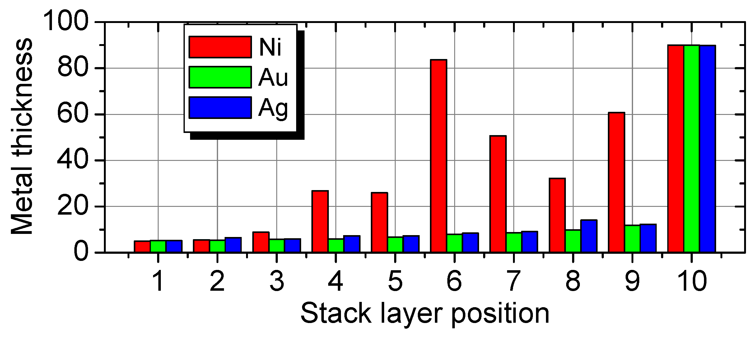
Disclaimer/Publisher’s Note: The statements, opinions and data contained in all publications are solely those of the individual author(s) and contributor(s) and not of MDPI and/or the editor(s). MDPI and/or the editor(s) disclaim responsibility for any injury to people or property resulting from any ideas, methods, instructions or products referred to in the content. |
© 2023 by the authors. Licensee MDPI, Basel, Switzerland. This article is an open access article distributed under the terms and conditions of the Creative Commons Attribution (CC BY) license (https://creativecommons.org/licenses/by/4.0/).