Article

Design of All-Optical Subtractors Utilized with Plasmonic Ring Resonators for Optical Computing

1
College of Electronics and Information Engineering, Southwest University, Chongqing 400715, China
2
School of Computer and Information Science, Chongqing Normal University, Chongqing 401331, China
3
Chongqing Key Laboratory of Nonlinear Circuits and Intelligent Information Processing, Chongqing 400715, China
*
Author to whom correspondence should be addressed.
Photonics 2023, 10(7), 724; https://doi.org/10.3390/photonics10070724
Submission received: 21 May 2023 / Revised: 12 June 2023 / Accepted: 22 June 2023 / Published: 25 June 2023
(This article belongs to the Special Issue Surface Plasmon)

Abstract

:
In this paper, a novel plasmonic all-optical half-subtractor and full-subtractor are designed for optical computing. The structure of plasmonic subtractors consists of a metal–insulator–metal (MIM) waveguide and rectangular ring resonators covered by a graphene layer. Due to the nonlinear optical properties of graphene, the states of the plasmonic resonators can be controlled by the pump intensity of a pump beam focused on the graphene layer. The resonators can work as all-optical switches with an ultra-fast response time to constitute optical logic devices according to the directed logic mechanism. A finite-difference time-domain method is utilized to numerically investigate the transmission of the output signals which represent the results of subtraction operations. Simulation results obtained indicate that the proposed plasmonic devices have the ability to implement half-subtraction and full-subtraction with a small feature size and fast response time, and provide a new concept and method for the design and realization of optical computing devices.

1. Introduction

With the rapid development of machine-learning techniques, especially artificial neural networks (ANNs), the need for high-speed and energy-efficient computing architectures has become more and more urgent [1,2]. However, as Moore’s law is slowing and nearing its end, traditional electronic computing circuits are faced with increasingly difficult challenges, such as the unavoidable physical limits of nano-fabrication technique [3]. Moreover, the time delay of each electronic logic device cascaded to enable computing operations will inevitably accumulate, resulting in degradation of the circuit performance [4]. Therefore, it is urgently required to develop a novel mechanism which can overcome the limitations of traditional electronic systems to enable computing operations.
Owing to the unique properties of photons as opposed to electrons, optical computing, which uses light to carry information and implement logic computing, has advantages, such as large bandwidth, low latency, high speed of signal propagation, and the capability of parallel processing [5,6,7,8,9]. Thus, optical computing is considered to increase the efficiency of information processing beyond traditional electron computing [10]. It has huge potential in various fields, especially those with requirements for high-throughput and on-the-fly data processing, such as ANNs. Optical neural networks (ONNs), which build ANNs with optical computing devices, offer a promising and effective approach to further improve the performance of ANNs [11,12,13]. Optical computing will become an important core technology for the next stage of information processing.
One of the most fundamental and crucial technologies associated with optical computing is optical logic operation [14]. There is a strong and growing interest by researchers to develop optical logic devices with better performance to meet different requirements. Schemes which underpin optical logic operations widely employ the mechanism of directed logic (DL) [15]. In DL, the optical signal is transmitted in the optical network composed of optical switches whose status is controlled by electrical signals. The optical signals output from the ports represent the logical operation results of the electrical input signals [16,17]. Since the electrical signals applied in all optical switches are parallel, change to each switch state can be implemented almost simultaneously such that their operations are independent of each other. Then, thanks to the high transmission speed of photons, the computed results can be propagated in the optical network much faster than by electrons in wires. Moreover, the latency of each switch does not accumulate so that the overall delay of the device is drastically reduced [18,19,20]. The DL mechanism combines the advantages of maneuverability of electrical signals and the high performance of optical signals. It is believed to be the best candidate for the next-generation computer [9,21].
Due to the great significance of DL in optical computing, a lot of work has been carried out on DL in recent years. Firstly, researchers designed and manufactured optical devices to implement directed logic gates, such as AND/NAND, OR/NOR, and XOR/XNOR [22,23,24]. Then, more complex optical devices were proposed to realize computing functions such as full-addition, numeric compare, and matrix-vector multiplication [25,26,27,28,29]. However, such optical devices based on a DL mechanism are almost always realized on a silicon-on-insulator (SOI) platform. While silicon photonics is recognized as a viable technology that could revolutionize traditional electronic information processing, it still suffers from a common problem of optical devices, that is, the diffraction limit. In other words, the implementation of sub-wavelength-scale optical logic devices is still difficult to achieve on silicon photonics [30]. Moreover, electro-optical switching in silicon-based optical logic devices has had negative effects on response time and power consumption [31,32]. Thus, it is critical to develop novel methods to enable optical computing. Surface plasmon polaritons (SPPs), localized surface electromagnetic waves along metal-dielectric interfaces, have the unique capacity to overcome diffraction-based limitations and can enable the control and manipulation of light at the nanoscale [33]. In addition, it has been demonstrated that, with the help of nonlinear materials, such as graphene, plasmonic all-optical switching can be achieved with an ultra-fast response time of picoseconds [34,35,36]. Therefore, plasmonic devices represent an ideal platform to implement ultra-fast logic operations for optical computing at the nanoscale.
Motivated by the aforementioned considerations, a novel all-optical half-subtractor and full-subtractor are proposed in this paper. Plasmonic rectangular ring resonators covered by a graphene layer work as all-optical switches to produce these subtractors according to the DL method. Due to the nonlinear optical properties of graphene, the intensity of a pump beam focused on the graphene layer can control the states of the all-optical switches with low power consumption and fast response time and can function as logic input. The transmission of output signals can represent the results of logical operations. The subtract operations are simulated and verified numerically using the finite-difference time-domain (FDTD) method. These proposed plasmonic devices not only implement subtract operations with a small feature size and fast response time, but also demonstrate effective applications of SPPs in optical computing devices.

2. Architecture and Theory

2.1. All-Optical Switch

As we have described previously, the most critical part of the DL device is the optical switch. In this work, plasmonic rectangular ring resonators covered by graphene act as optical switches. Compared with circular and rectangular resonators, the bending structures in the corners of rectangular ring resonators are beneficial to enhance transmission [37]. Figure 1a is a 2D schematic diagram of the rectangular ring resonators (MRs). w is the width of the waveguides and the ring resonator. a and b are the lengths of the short and long sides, respectively. r represents the radius of the bending structure in the corners. d 1 and d 2 are the distances between the MRs and the waveguides. The insulator in the metal–insulator–metal (MIM) waveguides and the MRs is air, the refractive index of which is n = 1 . Silver is the metal material used due to its low ohmic loss. According to the Drude model [38], the permittivity of silver can be given by:
ε m ( ω ) = ε ω p 2 / ( ω 2 + i ω γ )
Here, ω is the angular frequency of the optical wave, the dielectric constant at infinite frequency is ε = 3.7 , the bulk plasma frequency is ω p = 1.38 × 10 16 Hz , and γ = 2.73 × 10 13 Hz is the electron collision frequency [39]. Based on these parameters, a material model of silver can be built for the simulations.
According to coupled mode theory [40], the transmission of SPPs waves in the rectangular ring resonator can be theoretical analyzed. S + n and S n ( n = 1 , 2 , 3 , 4 ) represent the input and output energy in the waveguides. The propagation direction of the incident wave is from the Input port to the Through port, and the subscript p = ± represents whether the propagation direction of the wave is the same as that of the incident wave. a, which displays the energy amplitudes, can be characterized as:
d a d t = ( j ω n 1 τ o 1 τ e 1 τ e ) a + 1 τ e 1 e j θ S + 1 + 1 τ e 2 e j θ S 2 + 1 τ e 3 e j θ S + 3 + 1 τ e 4 e j θ S 4
ω n is the resonance angular frequency of MR and θ represents the phase of the coupling coefficient. The other parameters in this equation represent the decay rate in MR. For instance, 1 / τ o is the decay rate due to the internal loss in the resonator. 1 / τ e and 1 / τ e are the decay rates due to the escape of power from the resonator into the waveguides. 1 / τ 1 , 3 represents the decay rate as the waves propagate along the direction of the incident wave in the waveguides. Conversely, 1 / τ 2 , 4 is the decay rate of waves that propagate in the opposite direction to the incident wave in the two waveguides. Additionally, according to the principle of energy conservation, the energy conversion equations can be obtained as:
S + 2 = S + 1 e j θ 1 τ e 1 a n
S 1 = S 2 e j θ 1 τ e 2 a n
S 3 = S 4 e j θ 1 τ e 4 a n
S + 4 = S + 3 e j θ 1 τ e 3 a n
Combining the Equations (2) to (6), we can determine the transmission of the SPPs waves at each output port of the MR.
T = S + 2 S + 1 2 = ( 1 1 τ e 1 j ( ω ω n ) + 1 τ o + 1 τ e + 1 τ e ) 2
D = S 3 S + 1 2 = ( 1 τ e 1 τ e 4 j ( ω ω n ) + 1 τ o + 1 τ e + 1 τ e ) 2
A = S + 4 S + 1 2 = ( 1 τ e 1 τ e 3 j ( ω ω n ) + 1 τ o + 1 τ e + 1 τ e ) 2
Among them, the transmission at the Through port (T) and the Drop port (D) is worthy of attention. It can been seen from the above equations that, when the frequency of the incident optical wave ω = ω n , the transmission at the Through port (T) will be minimized. Conversely, the Drop port will have the maximum transmission (D). This is the resonance state of the MR. Based on the above analysis, it is clear that, when the frequency of the incident optical wave is constant, the amount of energy output from each port of the resonator can be controlled by changing the resonance frequency of the MR ( ω n ). In this way, the MR can perform the function of an optical switch. As is well-known, the resonance wavelength of the rectangular ring resonator can be obtained by the resonant condition according to standing wave theory:
m · 2 π = 2 π λ n ( 2 a + 2 b + 2 π r ) R e ( N e f f ) + ϕ
Based on Equation (10), the resonance wavelength λ n is affected by different factors, such as the geometric parameters of the resonator, the refractive index (RI) of the material, etc. Since the structural parameters of the resonator are difficult to change after the device is manufactured, adjustment of the resonance wavelength by changing the RI of the material is currently the most common method used.
In traditional DL devices, control of the RI is usually achieved by the electro-optical effect, the response time of which can no longer meet requirements. Therefore, it is imperative to find a feasible method to control the RI with a faster response time. Recently, utilizing the nonlinear properties of graphene has been demonstrated to be a workable method by researchers. The RI of graphene can be changed by varying the pump intensity of the pump light irradiated on its surface due to its nonlinear optical properties [41,42]. According to the third-order nonlinear optical Kerr effect, the RI of monolayer graphene can be obtained as:
n = n 0 + n 2 I
Here, n 0 and n 2 are the linear and nonlinear RI of graphene, respectively. I represents the pump intensity of the pump light. The giant negative nonlinear RI of graphene has been confirmed in the visible and near-infrared regime using many methods, such as the Z-scan method, the four-wave mixing technique, and the optical Kerr gate experiment [43,44,45,46]. In this work, n 0 = 2.4 and n 2 = 1.2 × 10 7 cm 2 /W based on previous experimental results [45,47]. In the plasmonic device, the field reinforcement caused by plasmonic resonances can induce a nonlinearity enhancement of graphene. A stronger interaction between the plasmonic resonances and graphene can be induced by the coupling between SPPs and the charge carriers of graphene. This process will create an enormous increment in the RI of the ambient dielectric surroundings, which can induce variation in the resonance properties of the plasmonic nanostructures [48]. This has been confirmed by the experimental measurements of Reckinger et al. [49]. Therefore, the resonance wavelength of the plasmonic resonator can be tuned with the help of graphene to perform the function of an optical switch.
Moreover, the response time of a plasmonic device is determined by the nonlinear response time of the nonlinear optical Kerr material [50]. So, in our work, the response time of the proposed plasmonic all-optical switch depends on the nonlinear optical response of graphene. There are two processes for the nonlinear optical response of graphene: first, the electron–hole pairs are excited to achieve another Fermi–-Dirac distribution through photonics thermalization by carrier–carrier intraband scattering and phonon emission; this process takes hundreds of femtoseconds. Then, interband carrier relaxation and hot phonon emission occurs, which takes around one to two picoseconds [46,51]. Therefore, the total nonlinear optical response time of graphene is about 2 ps. This unique characteristic of graphene provides a viable and effective method to develop various optical devices with an ultra-fast response time, such as an all-optical switch. For instance, Zhang et al. proposed a low power and ultra-fast all-optical multi-channel plasmonic switch at telecommunication wavelengths utilizing graphene covered on the cavity [34]. Ono et al. proposed an ultra-fast and energy-efficient all-optical switch with graphene-loaded deep-subwavelength plasmonic waveguides [35]. Wang et al. designed a three-channel all-optical plasmonic switcher whose cavity is covered by graphene; the switcher can realize ultra-fast switching via pump light [52]. Moreover, graphene has also been used to achieve all-optical tunable on-chip plasmon-induced transparency with ultra-fast response time [42,53,54]. All the above studies have demonstrated that an ultra-fast response time can be achieved using the nonlinear properties of graphene in plasmonic devices. The ultra-fast response time of the device proposed in this work is also based on the same mechanism.
Hence, in our proposed plasmonic device, the rectangular ring resonator is covered by a single layer of graphene to work as an all-optical switch whose switch status can be controlled by the pump light. Figure 1b shows a 3D schematic diagram of this plasmonic all-optical switch. The thickness of the silver slab is 100 nm based on previous experimental research and the thickness of the monolayer graphene is assumed to be 0.5 nm [32]. In order to verify the switch functions, it is simulated numerically using the FDTD method. In many studies concerning plasmonic devices with nonlinear optical Kerr materials, researchers have usually paid more attention to change in the plasmonic nanostructure resonance properties induced by variations in RI due to the nonlinear properties of the materials used, such as graphene. Usually, the graphene covering the top of the plasmonic resonators will be treated as an optical nonlinear material filling the resonators during simulations. The experimental results of some studies are in good agreement with the simulated results obtained using this method [31,50,55]. As an approximation, which previous related works have usually adopted, we focus on the resonance properties and transmission situation of the proposed plasmonic resonator when the RI of graphene changes due to its nonlinear optical Kerr effect.
According to Equation (10), the resonance wavelength of a plasmonic rectangular ring resonator is related to the RI of the dielectric material. Based on the analysis above, we know that the resonator is covered by a single layer of graphene, which will cause change in the RI of the dielectric material under different pump intensities. Therefore, the resonance properties of the plasmonic rectangular ring resonator are changed accordingly—intuitively, the resonance wavelength will shift to different values. So when the intensity of the pump light changes, the transmission of the same wavelength optical signal will also change. The proposed plasmonic all-optical switch is realized in this way. Figure 2a shows the simulation results for one kind of proposed all-optical switch. The structural parameters of this plasmonic resonator are as follows: The widths of the bus waveguide and resonators are w = 50 nm. The side lengths a and b are 200 nm and 350 nm. The outer and inner radii of the bending structure in the corners are 100 nm and 50 nm, respectively (r = 75 nm). The coupling distances between the bus waveguides and the resonators d 1 ( 2 ) are both 20 nm. It can been seen from the simulated transmission spectra that, when the intensity of the pump light focused on the graphene layer is 0 MW/cm 2 , the transmission at the Through port of the resonator is 98.21% and that of the Drop port is 0.04% at a wavelength of 850 nm. In this case, 850 nm is not the resonance wavelength of the plasmonic resonator and the plasmonic resonator is in a non-resonance state. So when the SPPs waves with 850 nm pass through the resonator, they will not couple into the resonator and propagate along with the bus waveguide. So, most power will be output from the Through port and no power will be detected at the Drop port. When the intensity of the pump light increases to 10.53 MW/cm 2 , the transmission at the Through and Drop ports changes to 1.55% and 75.01%. This is because the RI of graphene and the dielectric material in the resonator both change, and the resonance wavelength of the plasmonic resonator shifts to 850 nm. When the SPPs waves with 850 nm pass through the resonator, the resonator changes to a resonance state. Most SPPs waves with wavelength 850 nm will couple into the resonator and, finally, output from the Drop port. That is, by varying the pump intensity of the pump light, the switching states of the device are significantly changed, so it can work as an all-optical switch. Based on the computational functions to be achieved, we designed another kind of all-optical switch with alternative structural parameters whose simulated transmission spectra are shown in Figure 2b. In this structure, the widths of the bus waveguide and the resonators are w = 50 nm. The short side length a is 200 nm and the long side length b is 362 nm. The outer and inner radii of the bending structure in the corners are 100 nm and 50 nm (r = 75 nm). The coupling distances d 1 and d 2 are 35 nm and 25 nm, respectively. According to the simulated transmission spectra of the second kind of plasmonic all-optical switch shown in Figure 2b, when the pump intensity increases from 0 MW/cm 2 to 10.53 MW/cm 2 , the transmission at the Through port changes from 98.54% to 42.19%. The transmission at the Drop port increases from 0.09% to 41.75%. The SPPs waves can be output from the Through port and the Drop port of the resonator with similar transmission. In our FDTD simulation, the transmission is defined as a function which returns the amount of power transmitted through the power monitors, normalized to the source power. This is consistent with the definition of transmission in the simulation software we used, Lumerical FDTD Solutions [56].

2.2. Plasmonic Subtractors

After verifying the feasibility of the plasmonic all-optical switches, we designed a plasmonic all-optical half-subtractor according to the DL mechanism. The structure diagram of the proposed half-subtractor is shown in Figure 3. It comprises three MRs covered by a graphene layer which work as all-optical switches. MR 1 and MR 2 are the first kind of all-optical switch whose transmission spectra are shown in Figure 2a. MR 3 is the second kind of all-optical switch whose transmission spectra are shown in Figure 2b. These optical switches are cascaded by MIM waveguides. In particular, a square resonator is introduced at the waveguide crossing to reduce crosstalk [57,58]. There is an input port where the optical wave is coupled into the device. In this plasmonic half-subtractor, the pump light signal focused on the surface of graphene covered on MR 1 represents the minuend A. When its pump intensity is 0 MW/cm 2 , the state of the input signal A is “0”. In contrast, when the pump intensity increases to 10.53 MW/cm 2 , the state of the input signal A is “1”. Similarly, the pump light focused on the surface of graphene covered on MR 2 represents the subtrahend B, and MR 3 is controlled by the pump light, which represents the signal A ¯ . In this way, the minuend A and the subtrahend B are input into this plasmonic half-subtractor by pumping light to control the states of the optical switches. Depending on the state of each optical switch, the SPPs waves can output from port D and B out . When the transmission of the signal output from port D is greater than the threshold value, the difference in half-subtraction is “1”. Otherwise, the difference in half-subtraction is “0”. Similarly, transmission of the signal output from port B out represents the output borrow results of the half-subtraction.
In the same way, we also propose a plasmonic full-subtractor. The structure diagram of the proposed plasmonic full-subtractor is shown in Figure 4. It comprises six MRs which work as all-optical switches. Among them, MR 1 , 2 , 3 , 4 , 6 are the first kind of all-optical switch whose transmission spectra are shown in Figure 2a. MR 5 is the second kind of all-optical switch, which has similar transmission at the Through and Drop ports in a resonance state. The pump light signal focused on the surface of graphene covered on MR 1 represents the minuend A. The pump light focused on the surface of graphene covered on MR 2 represents the previous borrow B in . MR 3 is controlled by the pump light which represents the signal A ¯ . The states of MR 4 , 6 depend on the subtrahend B. The pump light which controls the states of MR 5 represents the signal B ¯ . Thus, the propagation path of SPPs in the device is controlled by the input signal minuend A, subtrahend B, and previous borrow B in . When one of the transmissions at port D 1 , D 2 , or D 3 is greater than the threshold, the difference in full-subtraction is “1”. Otherwise, the difference in full-subtraction is “0”. Similarly, if one of the signals output from port B out 1 or B out 2 has a transmission larger than the threshold, the output borrow result of the full-subtraction is “1”. if the transmission of the signal is smaller than the threshold, the output borrow result of the full-subtraction is “0”.
According to the operating principle of the proposed plasmonic all-optical half-subtractor and full-subtractor, the equivalent logic diagrams are shown in Figure 5a,b, respectively. They can help us theoretically analyze the output results of the proposed plasmonic subtractors and verify their computational functions.

3. Results

In Section 2, the plasmonic all-optical switch, the basis of the proposed plasmonic subtractors, is theoreticallly analyzed using coupled mode theory and numerically verified by the FDTD method. We also briefly introduce the principle and implementation of all-optical subtractors based on plasmonic optical switches. In order to understand the details of the proposed plasmonic devices in implementing subtraction operations, the results of the transmission characteristics and magnetic field distributions are also studied using the FDTD method. The simulation software we used for the numerical study is Lumerical FDTD Solutions. A 2D FDTD method is utilized in this work to study the transmission characteristics of the proposed plasmonic subtractors. It has been reported that 2D FDTD simulation has the same, or very similar, results to 3D simulation in studies of the MIM waveguide plasmonic structure. During the FDTD simulations, the metal material silver is modeled using the Drude model [59]; the parameters of silver are taken from [60]. To ensure convergence of the simulation results, the mesh sizes in the x- and y-directions are chosen to be Δ x = Δ y = 5 nm. The absorbing boundary condition is set to be a perfectly matched layer (PML). The SPPs are excited by the standard mode source in Lumerical FDTD Solutions which injects a fundamental guided mode into the plasmonic waveguide [61], while the standard mode source injects a Gaussian pulse signal [62]. The injection axis is the x-axis and the direction is forward. The source ( P 1 ) is located in the waveguide near the input port, as shown in Figure 3 and Figure 4. The power monitors are located in the waveguide near the output ports, as shown in Figure 3 ( P 2 and P 3 ) and Figure 4 ( P 2 , P 3 , P 4 , P 5 , and P 6 ).

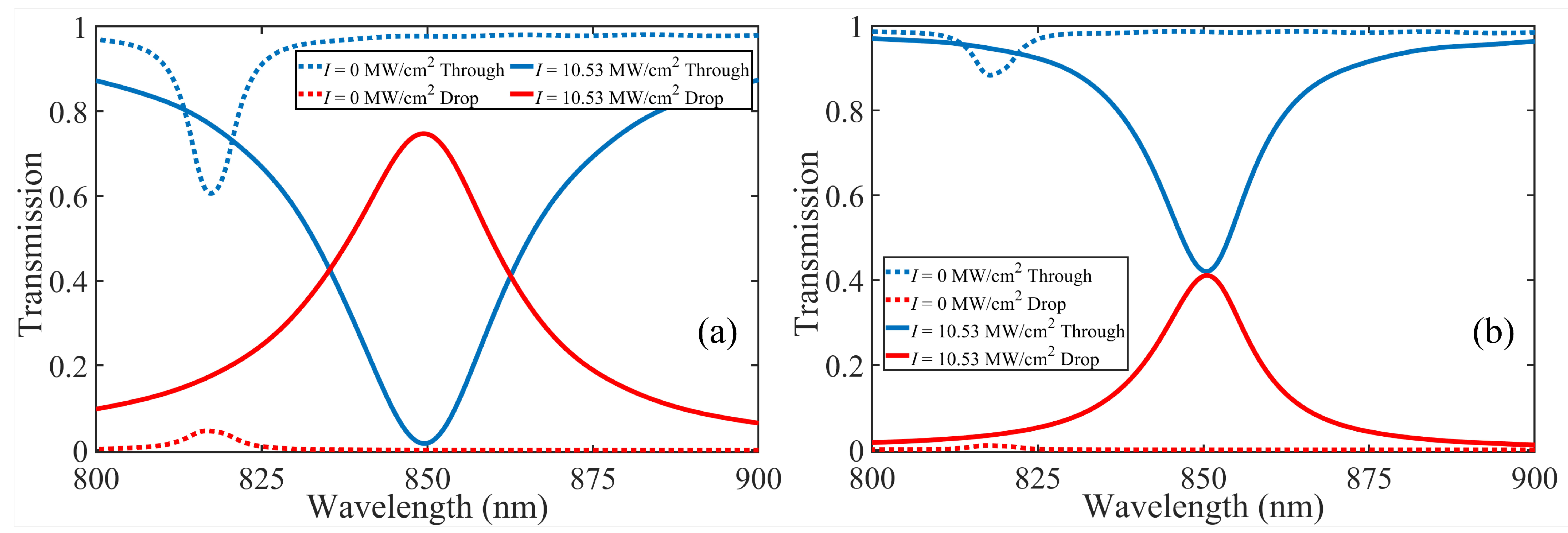
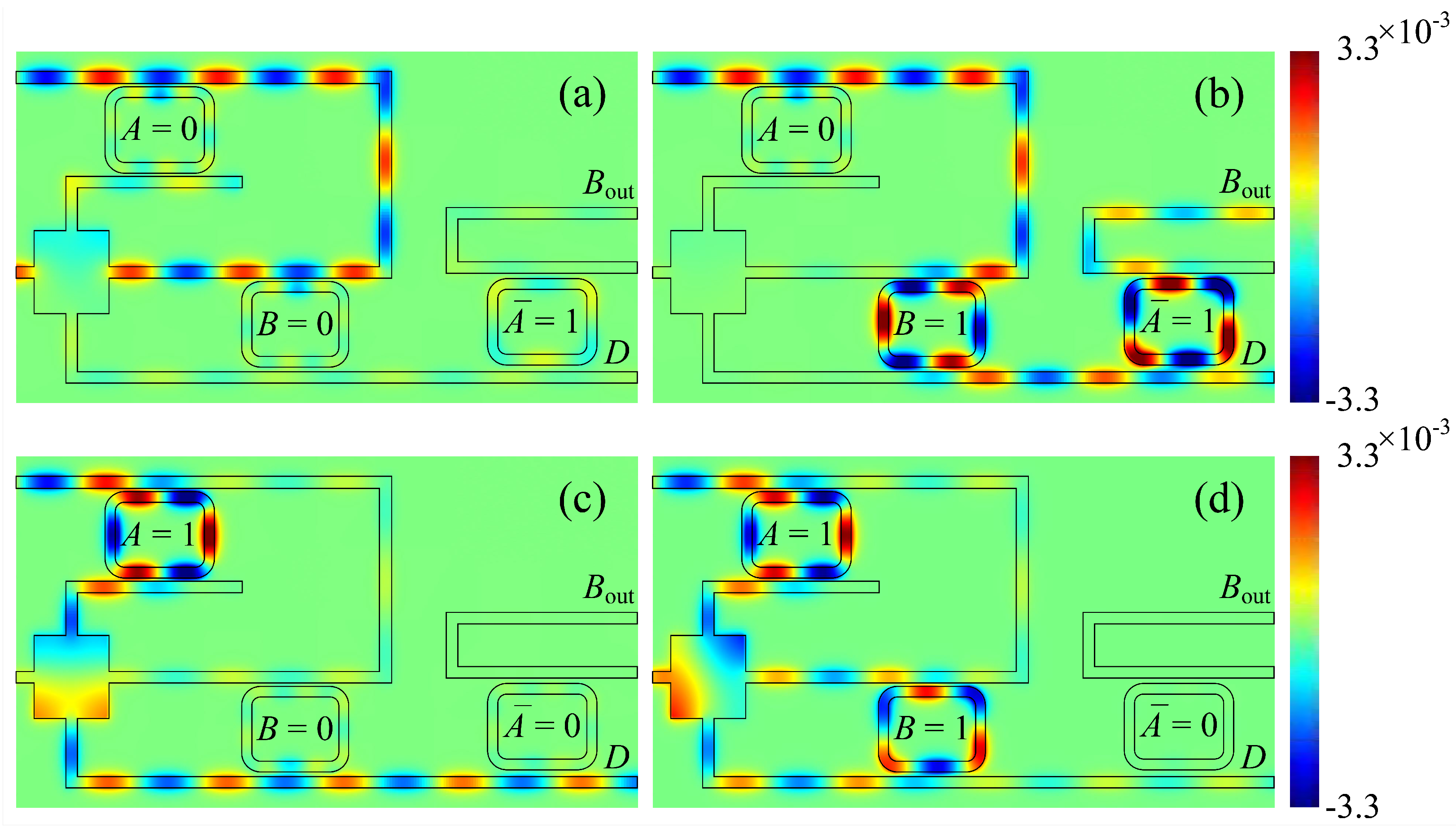
3.1. Simulated Results of the Plasmonic Half-Subtractor

As we have previously described, the minuend A and the subtrahend B are introduced into the proposed plasmonic half-subtractor by the pump intensity of the pump light focused on the surface of graphene covered on the MRs. The resonance wavelengths of all the MRs change according to the signal minuend A and the subtrahend B. This causes switching of the all-optical switch states. When optical waves with wavelength 850 nm are injected into the device from the input port, if the signal minuend A and the subtrahend B are both equal to “0”, the pump intensities of the pump light focused on MR 1 and MR 2 are 0 MW/cm 2 . The propagation paths of the SPPs will not change when they pass through these two MRs. They will directly output from the device along the bus waveguide, with no signal output from ports D and B out . According to the simulated spectra shown in Figure 6a, the transmission detected at ports D and B out is 0.593% and 0.652%. This result is in accordance with the Hz field distribution at 850 nm of the proposed half-subtractor shown in Figure 7a. Therefore, the difference and output borrow results of the half-subtraction for the input state A B = 00 are both “0”.
When the input minuend A is “0” and the subtrahend B is “1”, the pump intensity of the pump light focused on MR 1 remains 0 MW/cm 2 , and the pump intensity, which controls the state of MR 2 , increases to 10.53 MW/cm 2 . So the SPPs wave exits directly from the Through port of MR 1 , and, when it comes to the coupling area of MR 2 , it couples into MR 2 and exits from the Drop port of MR 2 since the resonance conditions of MR 2 are changed with the pump light focused on its graphene layer. Thus, the SPPs waves arrive at the coupling area of MR 3 . Since MR 3 is controlled by the signal A ¯ and A ¯ = 1 , the resonance states of MR 3 are also changed. Moreover, MR 3 is specially designed so that the Through and Drop ports have similar transmission in the resonance state. Therefore, the SPPs waves couple into MR 3 and output from port D and port B out . It can be inferred from the simulated results shown in Figure 6b that the transmission values at port D and port B out are 20.96% and 23.61%, respectively. The values are both larger than the threshold of 10%. This result can also be inferred from the Hz field distribution at 850nm shown in Figure 7b. So the difference and output borrow results of the half-subtraction for the input state A B = 01 are both “1”.
For the situation when the input minuend A is 1 and the subtrahend B is 0, the pump intensities controlling the state of MR 1 , MR 2 , and MR 3 are 10.53 MW/cm 2 , 0 MW/cm 2 , and 0 MW/cm 2 . So the SPPs waves will couple into MR 1 and exit from its Drop port. Then, as the states of MR 2 and MR 3 are non-resonant, most SPPs waves will continue to travel along the bus waveguide and output directly from port D with transmission 56.79%. The transmission at port B out is 0.002%, which means that there is almost no SPPs wave output from the port B out . This coincides with the simulated transmission spectra in Figure 6c and the field distribution in Figure 7c. So the result of half-subtraction for the input state A B = 10 is “10”.
As the input minuend A and the subtrahend B are both equal to “1”, the pump intensities applied to MR 1 and MR 2 are 10.53 MW/cm 2 . These MRs are both switched to the resonant state. Hence, the SPPs waves will couple into the MR 1 , 2 and output from their Drop port. Almost no energy is emitted from ports D and B out . The transmissions detected in ports D and B out are 0.692% and 0.001% according to the simulated transmission spectra shown in Figure 6d. The field distribution in Figure 7d also confirms this result. So the difference and output borrow results of the half-subtraction for the input state A B = 1 are both “0”.
Table 1 shows the transmission at the port D and B out as well as the logical Boolean value it represents for each input state based on the FDTD simulated results. According to Table 1, we can conclude that the proposed plasmonic device can implement the half-subtraction operation.

3.2. Simulated Results of Plasmonic Full-Subtractor

Similar to the working principle of the half-subtractor, the logic input signals of the full-subtractor are also fed into the proposed device in the form of pump intensities. The pump light signal focused on the surface of graphene covered on MR 1 represents the minuend A. MR 2 is controlled by the pump light, which represents the previous borrow B in . MR 3 is controlled by the pump light, which represents the signal A ¯ . The states of MR 4 , 6 both depend on the subtrahend B. The pump light which controls the states of MR 5 represents the signal B ¯ . As long as one of the transmissions at ports D 1 , D 2 , or D 3 is larger than the threshold of 10%, the difference in full-subtraction is “1”. If the transmission detected at port B out 1 or B out 2 is larger than 10%, the output borrow result of the full-subtraction is “1”.
When the input minuend A and the previous borrow B in are both “0”, the pump intensities focused on MR 1 and MR 2 are 0 MW/cm 2 and they are in a non-resonance state. So, the SPPs waves will not couple into MR 1 and MR 2 . They will arrive at the coupling area of MR 4 directly through the bus waveguide. If the subtrahend B is also “0”, the pump intensity which controls the state of MR 4 is 0 MW/cm 2 . The SPPs waves will output from the Through port of MR 4 and no power will be detected at port D 1 and port B out 1 . This coincides with the FDTD simulated results shown in Figure 8a, showing that the transmissions at D 1 and B out 1 are both 0.734%. Meanwhile, the transmissions at all other ports are close to 0, which is less than the threshold 10%. Therefore, the difference and output borrow results of the full-subtraction for the input state A B B in = 000 are both “0”. Moreover, if the subtrahend B is “1”, the pump light focused on the graphene layer of MR 4 is 10.53 MW/cm 2 . So, MR 4 changes to a resonance state and the SPPs waves will couple into MR 4 and output from port D 1 and port B out 1 at a similar transmission due to the splitter structure. The simulated transmission spectrum of the input states A B B in = 010 is shown in Figure 8b. The transmissions at port D 1 and port B out 1 are both 22.87%. So, the difference and output borrow results of the full-subtraction for the input state A B B in = 010 are “11”. The above results can also be obtained from the Hz field distribution at 850 nm shown in Figure 9a,b.
When the input minuend A is “0” and the previous borrow B in is “1”, the pump intensity of the pump light focused on MR 1 remains 0 MW/cm 2 , and the pump intensity which controls the state of MR 2 increases to 10.53 MW/cm 2 . MR 3 also changes to a resonance state since its control signal A ¯ is “1”. Therefore, the SPPs waves will not couple into MR 1 , but couple into MR 2 as well as MR 3 , and eventually arrive at the coupling area of MR 5 . As the subtrahend B is “0”, the pump intensity which controls the state of MR 5 is 10.53 MW/cm 2 since it represents the signal B ¯ . The RI of MR 5 changes under the influence of graphene, which puts it in a resonance state. So the SPPs waves will couple into MR 5 . Since MR 5 is specially designed to have similar transmission at its Though and Drop ports, the SPPs waves output from port D 2 and B out 2 with transmission are 16.75% and 16.23%, respectively, which can be obtained from the simulated transmission spectra shown in Figure 8c and the Hz field distribution shown in Figure 9c. So the difference and output borrow bits of the full-subtraction operation for the input state A B B in = 001 are “11”. As for the situation when the subtrahend B is “1”, MR 5 is in a non-resonance state since its control signal B ¯ = 0 . So, the SPPs waves will all output from the Through port of MR 5 , in other words, port B out 2 of the whole device. Almost no power can be observed at port D 2 . It can be inferred from Figure 8d that transmission at port B out 2 is 38.98%, while the transmission at the other ports has a value close to 0, as the input state A B B in = 011 . Therefore, the difference and output borrow results of the full-subtraction for the input state A B B in = 011 are “01”.
The situation is relatively simple for the input state A B B in = 100 and 110. Firstly, When the SPPs waves passes through the coupling area of MR 1 , it couples into the resonator and mostly outputs from the Drop port since the resonance wavelength of MR 1 changes to 850 nm under the influence of the pump intensity which represents the signal minuend A = 1 . Then, the pump intensities of the signals which control the resonance state of MR 2 and MR 3 are maintained as 0 MW/cm 2 since the previous borrow B in and A ¯ are both equal to “1”. So the SPPs waves will propagate along with the bus waveguide and directly pass through MR 2 as well as MR 3 . If the subtrahend B is “0”, which means the pump intensity applied to MR 6 is 0 MW/cm 2 , the waves will mostly output from port D 3 . According to the simulated transmission spectra of the input state A B B in = 100 , as shown in Figure 8e. The transmission detected at port D 3 is 51.98%, while the other ports have no transmission larger than the threshold of 10%, so the difference and output borrow results of the full-subtraction for the input state A B B in = 100 are “10”. Moreover, if the subtrahend B is “1”, which means the pump intensity applied to MR 6 is 10.53 MW/cm 2 , the SPPs waves will couple into MR 6 and mostly output from the Drop port. In this case, almost no SPPs will output from the ports that represent the result of full-subtraction, such as D 1 , D 2 , D 3 , B out 1 , and B out 2 . This is confirmed by the simulated transmission spectra and Hz field distribution for the input state A B B in = 110 shown in Figure 8f and Figure 9f. Hence, the operation results of the proposed device when the input state is A B B in = 110 are difference bit = 0 and output borrow bit = 0.
Compared with the cases of A B B in = 100 or A B B in = 110 , the SPPs waves will couple into the MR 2 after they output from the Drop port of MR 1 for the input case A B B in = 101 or A B B in = 111 . This is because the pump intensity which controls the state of MR 2 increases to 10.53 MW/cm 2 since the previous borrow B in = 1 . The final results depend on the signal represented by the subtrahend B. If the subtrahend B = 0 , the SPPs waves will pass through MR 4 and output from its Through port. Almost no waves output from the ports represents the operation result. In this situation, the final result of full-subtraction for the input state A B B in = 101 is difference bit = 0 and output borrow bit = 0. If the subtrahend B = 1 , the SPPs waves will couple into MR 4 and output from its Drop port since the state of MR 4 changes to a resonance state. In this case, the final result of full-subtraction for the input state A B B in = 111 can be observed from the transmissions at port D 1 and B out 1 . According to the simulated transmission spectra and the Hz field distribution for the input state A B B in = 111 shown in Figure 8h and Figure 9h, the transmissions detected at D 1 and B out 1 are both 16.11%, which is larger than the threshold of 10%. So, the operation results of the proposed full-subtractor when the input state is A B B in = 111 are difference bit = 1 and output borrow bit = 1.
Table 2 shows the transmission at each port in the operation of the proposed plasmonic full-subtractor based on the the simulated results using the FDTD method. Based on the comparisons between the transmission and the threshold of 10%, the corresponding logic Boolean value can also be obtained from Table 2. As we have mentioned previously, as long as one of the transmissions at ports D 1 , D 2 , or D 3 is larger than 10%, the difference in full-subtraction is “1”. If the transmissions detected at port B out 1 or B out 2 are larger than the threshold, the output borrow result of the full-subtraction is “1”. Based on the above analyses, we can draw the conclusion that the proposed plasmonic device can accurately realize the logic functions of the full-subtractor.

4. Comparisons

A comparison between our work and previous studies about optical computing devices can show more intuitively the differences between them. Therefore, the proposed plasmonic half-subtractor and full-subtractor are compared to previous works about plasmonic logic computing devices, as depicted in Table 3.

5. Conclusions

In conclusion, a novel all-optical half-subtractor and full-subtractor were designed based on plasmonic ring resonators to combine the advantages of all-optical switches and the DL mechanism. Due to the nonlinear optical properties of graphene, the states of the plasmonic resonator can be controlled by applying the pump light whose pump intensity represents the logic input on the covered graphene layer. Hence, the plasmonic ring resonators can work as all-optical switches with ultra-fast response time. Then, according to the DL mechanism in realizing optical logic devices, the plasmonic ring resonators covered by the graphene layer are cascaded with the MIM waveguide to constitute an all-optical half-subtractor and full-subtractor. The numerical simulation results using the FDTD method indicate that these plasmonic devices can accurately realize the operations of half-subtraction and full-subtraction for all input logic states. The proposed plasmonic devices can not only implement subtract operations with a small feature size and ultra-fast response time, but also provide a new concept and method for the design and realization of optical computing devices. They can extend the application scenario of SPPs in the field of optical information processing.

Author Contributions

Conceptualization, Y.Y. and T.S.; methodology, Y.Y.; validation, Y.Y., T.S. and Y.X.; formal analysis, Y.Y. and T.S.; investigation, Y.Y.; resources, Y.X.; data curation, Y.Y., T.S. and Y.X.; writing—original draft preparation, Y.Y.; writing—review and editing, Y.Y. and T.S.; visualization, Y.Y. and T.S.; supervision, Y.X.; project administration, Y.X. and C.L.; funding acquisition, T.S. and Y.X. All authors have read and agreed to the published version of the manuscript.

Funding

This research was funded by the Natural Science Foundation of Chongqing (CSTB2022NSCQ-MSX1200), the Science and Technology Research Program of Chongqing Municipal Education Commission (KJQN202200537), the Innovation Research 2035 Pilot Plan of Southwest University and Fundamental Research Funds for the Central Universities (SWU-XDPY22013), Chongqing Talent Plan (cstc2022ycjh-bgzxm0165), and Chongqing Normal University Ph.D. Start-up Fund (21XLB035).

Institutional Review Board Statement

Not applicable.

Informed Consent Statement

Not applicable.

Data Availability Statement

The data presented in this study are available from the corresponding author upon request.

Conflicts of Interest

The authors declare no conflict of interest.

References

  1. Jordan, M.I.; Mitchell, T.M. Machine learning: Trends, perspectives, and prospects. Science 2015, 349, 255–260. [Google Scholar] [CrossRef]
  2. Zuo, Y.; Li, B.; Zhao, Y.; Jiang, Y.; Chen, Y.-C.; Chen, P.; Jo, G.-B.; Liu, J.; Du, S. All-optical neural network with nonlinear activation functions. Optica 2019, 6, 1132–1137. [Google Scholar] [CrossRef]
  3. Waldrop, M.M. The chips are down for Moore’s law. Nature 2016, 530, 4. [Google Scholar] [CrossRef] [Green Version]
  4. Qiu, C.; Xiao, H.; Wang, L.; Tian, Y. Recent advances in integrated optical directed logic operations for high performance optical computing: A review. Front. Optoelectron. 2022, 15, 1–17. [Google Scholar] [CrossRef] [PubMed]
  5. Dong, W.; Lei, L.; Chen, L.; Yu, Y.; Zhang, X. All-optical 2 × 2-bit multiplier at 40 gb/s based on canonical logic units-based programmable logic array (clus-pla). J. Light. Technol. 2020, 38, 5586–5594. [Google Scholar] [CrossRef]
  6. Touch, J.; Badawy, A.-H.; Sorger, V.J. Optical computing. Nanophotonics 2017, 6, 503–505. [Google Scholar] [CrossRef]
  7. Ying, Z.; Dhar, S.; Zhao, Z.; Feng, C.; Mital, R.; Chung, C.-J.; Pan, D.Z.; Soref, R.A.; Chen, R.T. Electro-optic ripple-carry adder in integrated silicon photonics for optical computing. IEEE J. Sel. Top. Quantum Electron. 2018, 24, 7600310. [Google Scholar] [CrossRef]
  8. Qian, C.; Lin, X.; Lin, X.; Xu, J.; Sun, Y.; Li, E.; Zhang, B.; Chen, H. Performing optical logic operations by a diffractive neural network. Light Sci. Appl. 2020, 9, 59. [Google Scholar] [CrossRef] [Green Version]
  9. Caulfield, H.J.; Dolev, S. Why future supercomputing requires optics. Nat. Photonics 2010, 4, 261–263. [Google Scholar] [CrossRef]
  10. Cheng, Z.; Ríos, C.; Youngblood, N.; Wright, C.D.; Pernice, W.H.P.; Bhaskaran, H. Device-Level photonic memories and logic applications using phase-change materials. Adv. Mater. 2018, 30, 1802435. [Google Scholar] [CrossRef] [Green Version]
  11. Zhang, W.; Huang, C.; Peng, H.-T.; Bilodeau, S.; Jha, A.; Blow, E.; Lima, T.F.D.; Shastri, B.J.; Prucnal, P. Silicon microring synapses enable photonic deep learning beyond 9-bit precision. Optica 2018, 9, 579–584. [Google Scholar] [CrossRef]
  12. Ohno, S.; Tang, R.; Toprasertpong, K.; Takagi, S.; Takenaka, M. Si microring resonator crossbar array for on-chip inference and training of the optical neural network. ACS Photonics 2022, 9, 2614–2622. [Google Scholar] [CrossRef]
  13. Liu, X.; Zhang, D.; Wang, L.; Ma, T.; Liu, Z.; Xiao, J.-J. Parallelized and Cascadable Optical Logic Operations by Few-Layer Diffractive Optical Neural Network. Photonics 2023, 10, 503. [Google Scholar] [CrossRef]
  14. Miller, D.A.B. Are optical transistors the logical next step? Nat. Photonics 2010, 4, 3–5. [Google Scholar] [CrossRef]
  15. Hardy, J.; Shamir, J. Optics inspired logic architecture. Opt. Express 2007, 15, 150–165. [Google Scholar] [CrossRef]
  16. Zhang, F.; Zhang, L.; Yang, L. Directed logic circuits based on silicon microring resonators. Laser Optoelectron. Prog. 2014, 51, 110004. [Google Scholar] [CrossRef] [Green Version]
  17. Qiu, C.; Ye, X.; Soref, R.; Yang, L.; Xu, Q. Demonstration of reconfgurable electro-optical logic with silicon photonic integrated circuits. Opt. Lett. 2012, 37, 3942–3944. [Google Scholar] [CrossRef] [Green Version]
  18. Ying, Z.; Zhao, Z.; Feng, C.; Mital, R.; Dhar, S.; Pan, D.Z.; Soref, R.; Chen, R.T. Automated logic synthesis for electro-optic logic-based integrated optical computing. Opt. Express 2018, 26, 28002–28012. [Google Scholar] [CrossRef]
  19. Ying, Z.; Feng, C.; Zhao, Z.; Soref, R.; Pan, D.Z.; Chen, R.T. Integrated multi-operand electro-optic logic gates for optical computing. Appl. Phys. Lett. 2019, 115, 171104. [Google Scholar] [CrossRef]
  20. Gostimirovic, D.; Ye, W.N. Ultracompact CMOS-compatible optical logic using carrier depletion in microdisk resonators. Sci. Rep. 2017, 7, 12603. [Google Scholar] [CrossRef] [PubMed] [Green Version]
  21. Soref, R.; De Leonardis, F.; Ying, Z.; Passaro, V.M.N.; Chen, R.T. Silicon-based group-IV OEO devices for gain, logic, and wavelength conversion. ACS Photonics 2020, 7, 800–811. [Google Scholar] [CrossRef]
  22. Tian, Y.; Zhang, L.; Ji, R.; Yang, L.; Zhou, P.; Chen, H.; Ding, J.; Zhu, W.; Lu, Y.; Jia, L.; et al. Proof of concept of directed or/nor and and/nand logic circuit consisting of two parallel microring resonators. Opt. Lett. 2011, 36, 1650–1652. [Google Scholar] [CrossRef] [PubMed] [Green Version]
  23. Tian, Y.; Zhang, L.; Xu, Q.; Yang, L. Xor/Xnor directed logic circuit based on coupled-resonator-induced transparency. Laser Photonics Rev. 2013, 7, 109–113. [Google Scholar] [CrossRef]
  24. Feng, C.; Ying, Z.; Zhao, Z.; Mital, R.; Pan, D.Z.; Chen, R.T. Analysis of microresonator-based logic gate for high-speed optical computing in integrated photonics. IEEE J. Sel. Top. Quantum Electron. 2020, 26, 8302208. [Google Scholar] [CrossRef]
  25. Ying, Z.; Wang, Z.; Zhao, Z.; Dhar, S.; Pan, D.Z.; Soref, R.; Chen, R.T. Silicon microdisk-based full adders for optical computing. Opt. Lett. 2018, 43, 983–986. [Google Scholar] [CrossRef]
  26. Law, F.K.; Uddin, M.R.; Hashim, H.; Won, Y.H. Demonstration of photonic micro-ring resonator based digital bit magnitude comparator. Opt. Quantum Electron. 2019, 51, 1–13. [Google Scholar] [CrossRef]
  27. Tian, Y.; Xiao, H.; Wu, X.; Liu, Z.; Meng, Y.; Deng, L.; Guo, X.; Liu, G.; Yang, J. Experimental realization of an optical digital comparator using silicon microring resonators. Nanophotonics 2018, 7, 669–675. [Google Scholar] [CrossRef]
  28. Xu, S.; Wang, J.; Zou, W. Optical Convolutional Neural Network with WDM-Based Optical Patching and Microring Weighting Banks. IEEE Photonics Technol. Lett. 2021, 33, 89–92. [Google Scholar] [CrossRef]
  29. Ma, P.Y.; Tait, A.N.; Lima, T.F.; Huang, C.; Shastri, B.J.; Prucnal, P.R. Photonic independent component analysis using an on-chip microring weight bank. Opt. Express 2020, 28, 1827–1844. [Google Scholar] [CrossRef]
  30. Gramotnev, D.K.; Bozhevolnyi, S.I. Plasmonics beyond the diffraction limit. Nat. Photonics 2010, 4, 83–91. [Google Scholar] [CrossRef]
  31. Yang, X.; Hu, X.; Yang, H.; Gong, Q. Ultracompact all-optical logic gates based on nonlinear plasmonic nanocavities. Nanophotonics 2017, 6, 365–376. [Google Scholar] [CrossRef]
  32. Fu, Y.; Hu, X.; Lu, C.; Yue, S.; Yang, H.; Gong, Q. All-optical logic gates based on nanoscale plasmonic slot waveguides. Nano Lett. 2012, 12, 5784–5790. [Google Scholar] [CrossRef]
  33. Cunningham, S.L.; Maradudin, A.A.; Wallis, R.F. Effect of a charge layer on the surface-plasmon-polariton dispersion curve. Phys. Rev. B 1974, 10, 3342–3355. [Google Scholar] [CrossRef]
  34. Zhang, Z.; Yang, J.; He, X.; Han, Y.; Zhang, J.; Huang, J.; Chen, D.; Xu, S. All-optical multi-channel switching at telecommunication wavelengths based on tunable plasmon-induced transparency. Opt. Commun. 2018, 425, 196–203. [Google Scholar] [CrossRef]
  35. Ono, M.; Hata, M.; Tsunekawa, M.; Nozaki, K.; Sumikura, H.; Chiba, H.; Notomi, M. Ultrafast and energy-efficient all-optical switching with graphene-loaded deep-subwavelength plasmonic waveguides. Nat. Photonics 2020, 14, 37–43. [Google Scholar] [CrossRef] [Green Version]
  36. Abbasi, M.M.; Darbari, S.; Moravvej-Farshi, M.K. Tunable plasmonic force switch based on graphene nano-ring resonator for nanomanipulation. Opt. Express 2019, 27, 26648–26660. [Google Scholar] [CrossRef]
  37. Tian, M.; Lu, P.; Chen, L.; Lv, C.; Liu, D. A subwavelength mim waveguide resonator with an outer portion smooth bend structure. Opt. Commun. 2011, 284, 4078–4081. [Google Scholar] [CrossRef]
  38. Wu, Y. High transmission efciency wavelength division multiplexer based on metal–insulator–metal plasmonic waveguides. J. Light. Technol. 2014, 32, 4844–4848. [Google Scholar]
  39. Chou Chao, C.-T.; Chou Chau, Y.-F. Highly Sensitive Multichannel Fano Resonance-Based Plasmonic Sensor for Refractive Index and Temperature Sensing Application. Photonics 2023, 10, 82. [Google Scholar] [CrossRef]
  40. Kristensen, P.T.; Lasson, J.R.; Heuck, M.; Gregersen, N.; Mørk, J. On the Theory of Coupled Modes in Optical Cavity-Waveguide Structures. J. Light. Technol. 2017, 35, 4247–4259. [Google Scholar] [CrossRef]
  41. Yang, X.; Hu, X.; Chai, Z.; Lu, C.; Yang, H.; Gong, Q. Tunable ultracompact chip-integrated multichannel flter based on plasmon-induced transparencies. Appl. Phys. Lett. 2014, 104, 221114. [Google Scholar] [CrossRef]
  42. Han, X.; Wang, T.; Liu, B.; He, Y.; Zhu, Y. Tunable triple plasmon-induced transparencies in dual t-shaped cavities side-coupled waveguide. IEEE Photonics Technol. Lett. 2016, 28, 347–350. [Google Scholar] [CrossRef]
  43. Geim, A.K.; Novoselov, K.S. The rise of graphene. Nat. Mater. 2007, 6, 183. [Google Scholar] [CrossRef] [PubMed]
  44. Hendry, E.; Hale, P.; Moger, J.; Savchenko, A.; Mikhailov, S. Coherent nonlinear optical response of graphene. Phys. Rev. Lett. 2010, 105, 212–217. [Google Scholar] [CrossRef] [Green Version]
  45. Zhang, H.; Virally, S.; Bao, Q.; Ping, L.K.; Massar, S.; Godbout, N.; Kockaert, P. Z-scan measurement of the nonlinear refractive index of graphene. Opt. Lett. 2012, 37, 1856–1858. [Google Scholar]
  46. Miao, L.; Jiang, Y.; Lu, S.; Shi, B.; Zhao, C.; Zhang, H.; Wen, S. Broadband ultrafast nonlinear optical response of few-layers graphene: Toward the mid-infrared regime. Photonics Res. 2015, 3, 214–219. [Google Scholar] [CrossRef]
  47. Kumar, N.; Kumar, J.; Gerstenkorn, C.; Wang, R.; Chiu, H.; Smirl, A.L.; Zhao, H. Third harmonic generation in graphene and few-layer graphite films. Phys. Rev. B 2013, 87, 121406(R). [Google Scholar] [CrossRef] [Green Version]
  48. Zhu, Y.; Hu, X.; Fu, F.; Yang, H.; Gong, Q. Ultralow-power and ultrafast all-optical tunable plasmon-induced transparency in metamaterials at optical communication range. Sci. Rep. 2013, 3, 2338. [Google Scholar] [CrossRef] [Green Version]
  49. Reckinger, N.; Vlad, A.; Melinte, S.; Colomer, J.-F.; Sarrazin, M. Graphene-coated holey metal flms: Tunable molecular sensing by surface plasmon resonance. Appl. Phys. Lett. 2013, 102, 211108. [Google Scholar] [CrossRef] [Green Version]
  50. Xie, J.; Niu, X.; Hu, X.; Wang, F.; Chai, Z.; Yang, H.; Gong, Q. Ultracompact all-optical full-adder and half-adder based on nonlinear plasmonic nanocavities. Nanophotonics 2017, 6, 1167–1173. [Google Scholar] [CrossRef]
  51. Nikolaenko, A.E.; Papasimakis, N.; Atmatzakis, E.; Luo, Z.; Shen, Z.X.; Angelis, F.; Boden, S.A.; Fabrizio, E.D.; Zheludev, N.I. Nonlinear graphene metamaterial. Appl. Phys. Lett. 2012, 100, 181109. [Google Scholar] [CrossRef] [Green Version]
  52. Wang, G.; Wu, T.; Shao, Y.; Jia, Y.; Gao, Y.; Gao, Y. Ultrafast and low-power multichannel all-optical switcher based on multilayer graphene. Appl. Opt. 2023, 62, 500–505. [Google Scholar] [CrossRef] [PubMed]
  53. Zhu, Y.; Hu, X.; Yang, H.; Gong, Q. On-chip plasmon-induced transparency based on plasmonic coupled nanocavities. Sci. Rep. 2014, 4, 3752. [Google Scholar] [CrossRef] [Green Version]
  54. Zhang, T.; Dai, J.; Dai, Y.; Fan, Y.; Han, X.; Li, J.; Yin, F.; Zhou, Y.; Xu, K. Dynamically tunable plasmon induced absorption in graphene-assisted metal odielectric grating. Opt. Express 2017, 25, 26221–26233. [Google Scholar] [CrossRef] [PubMed]
  55. Chai, Z.; Hu, X.; Zhu, Y.; Sun, S.; Yang, H.; Gong, Q. Ultracompact chip-integrated electromagnetically induced transparency in a single plasmonic composite nanocavity. Adv. Opt. Mater. 2014, 2, 320–325. [Google Scholar] [CrossRef]
  56. Transmission—Script Command. Available online: https://optics.ansys.com/hc/en-us/articles/360034405354-transmission-Script-command (accessed on 9 June 2023).
  57. Ye, Y.; Xie, Y.; Song, T.; Guan, N.; Lv, M.; Li, C. Integrated plasmonic full adder based on cascaded rectangular ring resonators for optical computing. Opt. Laser Technol. 2022, 156, 108479. [Google Scholar] [CrossRef]
  58. Lee, T.-W.; Lee, D.E.; Lee, Y.J.; Kwon, S.-H. Low cross-talk, deep subwavelength plasmonic metal/insulator/metal waveguide intersections with broadband tunability. Photonics Res. 2016, 4, 272–276. [Google Scholar] [CrossRef] [Green Version]
  59. Gugger, H.; Jurich, M.; Swalen, J.D.; Sievers, A.J. Observation of an index-of-refraction-induced change in the Drude parameters of Ag films. Phys. Rev. B. 1986, 34, 1322–1324. [Google Scholar] [CrossRef]
  60. Johnson, P.B.; Christy, R.W. Optical constants of the noble metals. Phys. Rev. B. 1972, 6, 4370–4379. [Google Scholar] [CrossRef]
  61. Mode Source—Simulation Object. Available online: https://optics.ansys.com/hc/en-us/articles/360034902153-Mode-source-Simulation-object (accessed on 8 June 2023).
  62. Dutta, S.; Zografos, O.; Gurunarayanan, S.; Radu, I.; Soree, B.; Catthoor, F.; Naeemi, A. Proposal for nanoscale cascaded plasmonic majority gates for non-Boolean computation. Sci. Rep. 2017, 7, 17866. [Google Scholar] [CrossRef] [Green Version]
  63. Lu, C.; Hu, X.; Yang, H.; Gong, Q. Chip-integrated ultrawide-band all-optical logic comparator in plasmonic circuits. Sci. Rep. 2014, 4, 3869. [Google Scholar] [CrossRef] [PubMed] [Green Version]
  64. Birr, T.; Zywietz, U.; Chhantyal, P.; Chichkov, B.N.; Reinhardt, C. Ultrafast surface plasmon-polariton logic gates and half-adder. Opt. Express 2015, 23, 31755–31766. [Google Scholar] [CrossRef] [PubMed]
  65. Kumar, S.; Singh, L.; Raghuwanshi, S.K. Design of plasmonic half-adder and half-subtractor circuits employing nonlinear effect in Mach–Zehnder interferometer. J. Comput. Electron. 2017, 16, 139–147. [Google Scholar] [CrossRef]
  66. Swarnakar, S.; Basha, S.C.A.; Azmathullah, S.; Prabhu, N.A.; Madhu, G.; Kumar, S. Improved design of all-optical half-adder and half-subtractor circuits using MIM plasmonic waveguides for optical networks. Opt. Quantum Electron. 2023, 55, 94. [Google Scholar] [CrossRef]
Figure 1. (a) 2D schematic diagram of the plasmonic rectangular ring resonator. (b) 3D schematic diagram of the plasmonic rectangular ring resonator covered by a graphene layer which works as an all-optical switch.
Photonics 10 00724 g001
Figure 2. (a) Transmission spectra of rectangular ring resonator covered by a layer of graphene for pump intensities I = 0 MW/cm 2 and I = 10.53 MW/cm 2 . (b) Transmission spectra of specially designed rectangular ring resonator covered by a layer of graphene for pump intensities I = 0 MW/cm 2 and I = 10.53 MW/cm 2 .
Photonics 10 00724 g002
Figure 3. 2D schematic diagram of the proposed plasmonic half-subtractor.
Photonics 10 00724 g003
Figure 4. 2D schematic diagram of the proposed plasmonic full-subtractor.
Photonics 10 00724 g004
Figure 5. (a) Equivalent logic diagram of the proposed plasmonic half-subtractor. (b) Equivalent logic diagram of the proposed plasmonic full-subtractor.
Photonics 10 00724 g005
Figure 6. Transmission spectra detected at port D and port B out of plasmonic half-subtractor for different input states: (a) A B = 00 . (b) A B = 01 . (c) A B = 10 . (d) A B = 11 .
Photonics 10 00724 g006
Figure 7. Hz field distribution of plasmonic half−subtractor at wavelength 850 nm for different input states: (a) A B = 00 . (b) A B = 01 . (c) A B = 10 . (d) A B = 11 .
Photonics 10 00724 g007
Figure 8. Transmission spectra detected at port D 1 , D 2 , D 3 , B out 1 and B out 2 of the plasmonic full-subtractor for different input states: (a) A B B in = 000 . (b) A B B in = 010 . (c) A B B in = 001 . (d) A B B in = 011 . (e) A B B in = 100 . (f) A B B in = 110 . (g) A B B in = 101 . (h) A B B in = 111 .
Photonics 10 00724 g008
Figure 9. Hz field distribution of the plasmonic full−subtractor at wavelength 850 nm for different input states: (a) A B B in = 000 . (b) A B B in = 010 . (c) A B B in = 001 . (d) A B B in = 011 . (e) A B B in = 100 . (f) A B B in = 110 . (g) A B B in = 101 . (h) A B B in = 111 .
Photonics 10 00724 g009
Table 1. Transmission and Boolean values at each port of the proposed half-subtractor for all input states.
Input StateTransmission at
Port D
Transmission at
Port B out
DifferenceOutput Borrow
A B = 00 0.593% (0)0.652% (0)00
A B = 01 20.96% (1)23.61% (1)11
A B = 10 56.79% (1)0.002% (0)10
A B = 11 0.692% (0)0.001% (0)00
Table 2. Transmission and Boolean values at each port of the proposed full-subtractor for all input states.
Input StateTransmission
at Port D1
Transmission
at Port D2
Transmission
at Port D3
Transmission
at Port Bout1
Transmission
at Port Bout2
DifferenceOutput Borrow
A B B in = 000 0.734% (0)0.069% (0)0.007% (0)0.734% (0)0.002% (0)00
A B B in = 010 22.87% (1)0.000% (0)0.000% (0)22.87% (1)0.429% (0)11
A B B in = 001 0.013% (0)16.75% (1)0.716% (0)0.013% (0)16.23% (1)11
A B B in = 011 0.531% (0)0.011% (0)0.022% (0)0.531% (0)38.98% (1)01
A B B in = 100 0.007% (0)0.139% (0)51.98% (1)0.007% (0)0.457% (0)10
A B B in = 110 0.143% (0)0.000% (0)0.175% (0)0.143% (0)0.553% (0)00
A B B in = 101 0.049% (0)0.006% (0)0.409% (0)0.049% (0)0.019% (0)00
A B B in = 111 16.11% (1)0.000% (0)0.075% (0)16.11% (1)0.069% (0)11
Table 3. Comparison between our proposed plasmonic subtractor and previous plasmonic optical computing devices.
WorksComputing FunctionsSimulation MethodMaterialsProposed StructureFootprintOperating WavelengthPerformance Measured
Ref. [50]Half-adder Full-adderFEM-2DGoldNonlinear Plasmonic NanocavitiesLess than 15 μ m × 15 μ m750 nmTransmission
Ref. [63]Comparator One-BitFEM-2DGoldMZI Based on MIM WaveguidesLess than 10 μ m × 10 μ m1000 nmIntensity and Contrast Ratio
Ref. [64]Half-adderFEM-2DGoldDielectric Crossed Plasmonic Waveguides10 μ m × 28 μ m800 nmIntensity
Ref. [65]Half-adder Half-subtractorFinite-difference Time-domainNot givenMZI Based on Plasmonic MIM Waveguides75 μ m × 8 μ m1550 nmOutput Optical Power
Ref. [66]Half-adder Half-subtractorFinite-difference Time-domainSilicon OxynitrideY-shaped Power Combiners Based on Plasmonic MIM Waveguides11 μ m × 6 μ m1550 nmIntensity
This workHalf-subtractorFinite-difference Time-domainSilverCascaded Plasmonic Rectangular Ring Resonator3.2 μ m × 1.6 μ m850 nmTransmission
This workFull-subtractorFinite-difference Time-domainSilverCascaded Plasmonic Rectangular Ring Resonator3.2 μ m × 1.6 μ m850 nmTransmission
Disclaimer/Publisher’s Note: The statements, opinions and data contained in all publications are solely those of the individual author(s) and contributor(s) and not of MDPI and/or the editor(s). MDPI and/or the editor(s) disclaim responsibility for any injury to people or property resulting from any ideas, methods, instructions or products referred to in the content.

