Review

Advanced Numerical Methods for Graphene Simulation with Equivalent Boundary Conditions: A Review

1
The Institute of Electromagnetics and Acoustics, Xiamen University, Xiamen 361005, China
2
The Fujian Provincial Key Laboratory of Electromagnetic Wave Science and Detection Technology, Xiamen University, Xiamen 361005, China
*
Author to whom correspondence should be addressed.
Photonics 2023, 10(7), 712; https://doi.org/10.3390/photonics10070712
Submission received: 30 April 2023 / Revised: 18 June 2023 / Accepted: 19 June 2023 / Published: 22 June 2023
(This article belongs to the Special Issue Recent Trends in Computational Photonics)

Abstract

:
Since the discovery of graphene, due to its excellent optical, thermal, mechanical and electrical properties, it has a broad application prospect in energy, materials, biomedicine, electromagnetism and other fields. A great quantity of researches on the physical mechanism of graphene has been applied to engineering in electromagnetism and optics. To study the properties of graphene, different kinds of numerical methods such as the mixed finite element method (Mixed FEM), the mixed spectral element method (Mixed SEM), Method of Auxiliary Sources (MAS), discontinuous Galerkin time-domain method (DGTD) and interior penalty discontinuous Galerkin time domain (IPDG) have been developed for simulating the electromagnetic field effects of graphene and equivalent boundary conditions such as impedance transmission boundary condition (ITBC), surface current boundary condition (SCBC), impedance matrix boundary condition (IMBC) and surface impedance boundary condition (SIBC) have been employed to replace graphene in the computational domain. In this work, the numerical methods with equivalent boundary conditions are reviewed, and some examples are provided to illustrate their applicability.

1. Introduction

Graphene [1,2,3,4,5] is an allotropy of 3-D crystal graphite, a true two-dimensional material composed of a single layer of carbon atoms. Due to its unique electrical, electromagnetic, and optical characteristics, it has attracted widespread attention, leading to the design of many new systems and equipment [6,7,8]. In 2010, Novoselov and Heim [1] won the Nobel Prize for their research and observation of graphene properties. Graphene exhibits semi metallic properties and has a strong bipolar electric field effect. And graphene has been shown to possess electrical properties similar to semiconductors (although with a zero band gap) [9,10,11,12]. Due to its excellent properties, many methods have been developed to fabricate graphene, such as micromechanical cleavage technique [13], chemical vapor deposition [14], solvent exfoliation [15,16], solvothermal method [17], etc. The development of preparation technology has made it easy to separate high-quality graphene, triggering a research boom in the 2-D material family. In fact, the optical properties generated by the unique electronic band structure of graphene are considered attractive features in the design of nanophotons and optoelectronic components [18,19,20]. Graphene has a strong interaction with electromagnetic fields, and its response to light is nonlinear, manifested by plasmonic characteristics. Graphene-based plasmonic can not only limit the electromagnetic field to a smaller transverse propagation range, but also modulate it over a wide frequency range through gating and chemical doping [21,22,23,24].
In the past few years, in addition to the physical research on graphene and graphene-based devices, another important topic has been the numerical simulation of graphene. Kubo formula puts forward the expression of graphene conductivity, which is a function formed by physical parameters such as wavelength, chemical potential and temperature [25,26,27,28]. A surface conductivity model is also proposed to describe graphene as an isotropic infinitesimal sheet. Although the model provides problematic results for some tests, the electromagnetic simulation of specific graphene devices still remains a challenge when it comes to practical graphene problems. Fortunately, with the development of computational electromagnetics, many efficient and accurate numerical methods have been proposed to analyze the electromagnetic response of graphene related devices. Among them, the most popular methods are the finite difference time domain method (FDTD), finite element method (FEM), DGTD and spectral element method (SEM) [29,30,31,32,33,34,35,36]. The numerical approaches of processing graphene include: (a) Taking graphene as a zero-thickness sheet [37,38,39]; (b) Graphene is regarded as a thin plate with finite thickness, and its surface conductivity is converted into a volumetric dielectric constant [40]. Due to the easy realization of (b), some published papers and commercial software model graphene as a thin sheet with limited thickness [41,42,43]. However, direct discretization of graphene thin plates results in extremely fine grids and a large number of unknowns. Especially in time-domain simulation, extremely small time steps are required to ensure stability, which consumes an enormous amount of CPU time and memory costs. Therefore, equivalent boundary conditions are preferred methods used to eliminate thin plates in the computational domain, which include impedance transmission boundary condition (ITBC) [44,45], surface current boundary condition (SCBC) [46], impedance matrix boundary condition (IMBC) [47] and surface impedance boundary condition (SIBC) [48,49]. These numerical methods and equivalent boundary conditions have been proved that can greatly improve the design and manufacturing speed.
In this review, we focus on the electromagnetic simulation of graphene, and select several numerical cases to show their serviceability in practical engineering applications.

2. Advanced Numerical Methods

With the development of computer performance and new efficient and accurate algorithms, electromagnetic numerical methods have become more applicable and efficient. In order to analyze the electromagnetic field interaction related to graphene and the shielding effect of graphene, several different numerical methods are used, including Mixed FEM, Mixed SEM, MAS, DGTD and IPDG, and equivalent boundary conditions such as ITBC, SCBC, IMBC and SIBC are introduced. Regardless of the boundaries used by these methods, a mathematical model is required to describe the conductivity of graphene. The following subsection depicts the mathematical model employed in this review.

2.1. Mathematical Model

The numerical methods listed above are commonly used to simulate graphene as a thin sheet with a conductivity that is both complex and dependent on frequency. The graphene surface conductivity is usually expressed using the Kubo formula [50,51,52]:
σ g = j e 2 ( ω j 2 Γ ) π ħ 2 [ 0 ε f d ( ε ) f d ( ε ) ( ω j 2 Γ ) 2 4 ( ε ħ ) 2 d ε + 1 ( ω j 2 Γ ) 2 0 ε ( f d ( ε ) ε f d ( ε ) ε ) d ε ]
where ε is the electron charge, ω is the radian frequent, Γ is the phenomenological scattering rate, ħ is the reduced Planck constant and e is the energy state. f d = ( e ( ε μ c ) / k B T + 1 ) 1 is the Fermi-Dirac distribution, where μ c is the chemical potential or Fermi level, T is the temperature and k B is the Boltzman constant. Equations (1) contains both intraband and interband contributions that is expressed as σ g = σ intra ( ω , μ c , Γ , T ) + σ i n t e r ( ω , μ c , Γ , T ) , where:
σ intra ( ω , μ c , Γ , T ) = 2 j e 2 T ħ 2 π ( ω j Γ ) ln 2 cos h ( μ c 2 T )
σ inter ( ω , μ c , Γ , T ) = e 2 4 ħ 1 2 + 1 π arctan ( ħ ω 2 μ c 2 T ) + j 2 π ln ( ħ ω + 2 μ c ) 2 ( ħ ω 2 μ c ) 2 + ( 2 T ) 2
The interband conductivity, which is smaller than the intraband conductivity, is in the order of magnitude of e 2 / ħ . The dielectric constant of graphene is determined by ε ^ = 1 j σ g / ( ε 0 ω τ ) . The electrons and holes close to the band edges “blocke” interband transitions at lower frequencies (i.e., in the THz range). Graphene exhibits the characteristics of a conductive film, and a straight forward Drude model is used to describe its conductivity (primarily caused by in-band contributions). The electrons and holes close to the band edges “blocke” interband transitions at lower frequencies

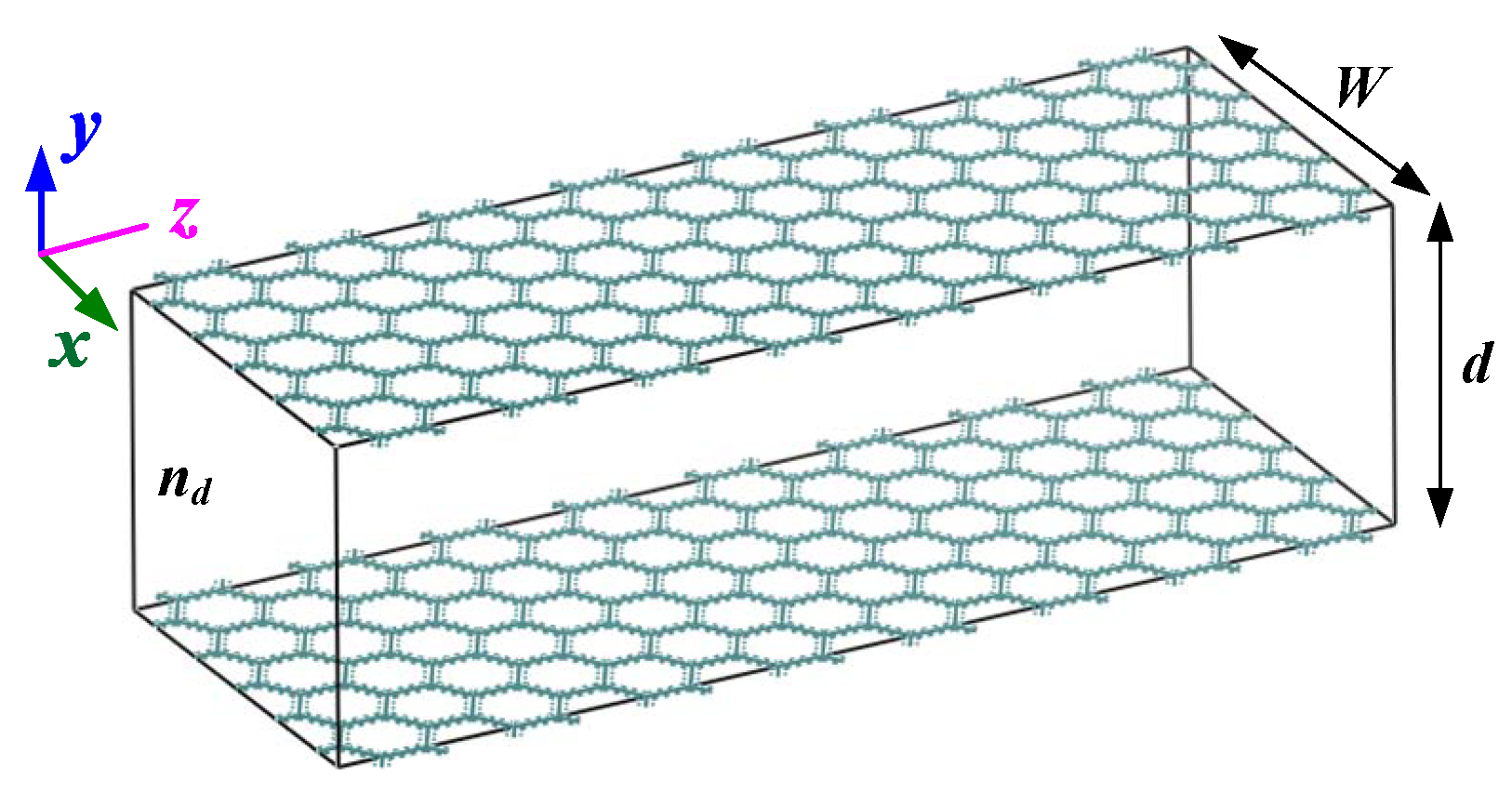
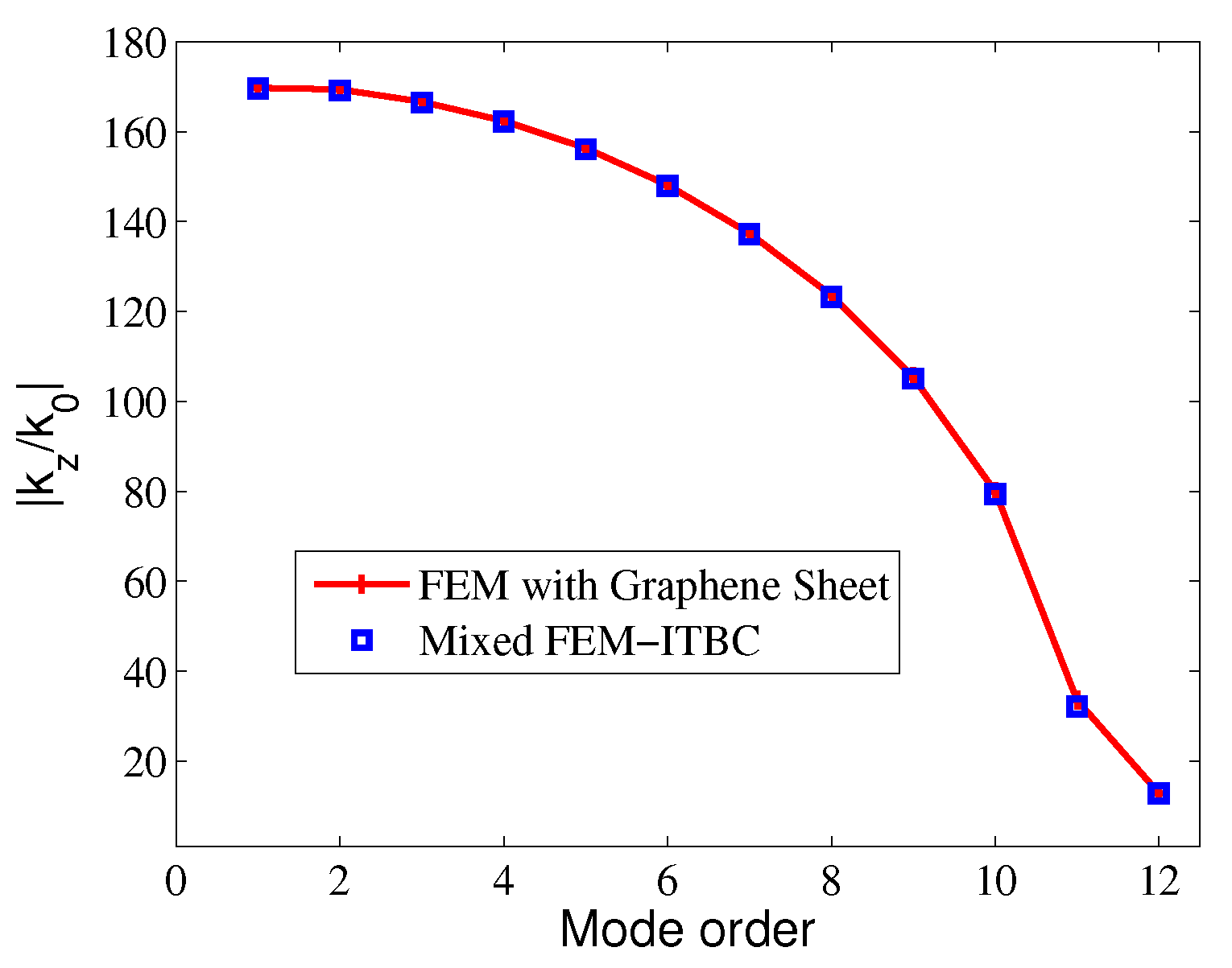
2.2. Mixed Finite Element Method

With the increasing complexity of microwave and optical waveguide structures, it is difficult to effectively conduct modal analysis of waveguide problem, which seriously delays the subsequent adjustment of geometric and material parameters in waveguide design. Scholars have developed different numerical methods to solve this problem, among which the FEM is a successful representative. The mathematical theory of the FEM was completed by Feng Kang and others scholars. Compared with the FDTD, the FEM utilizes unstructured meshes to discretize the computational domain, which is convenient for solving problems in complex calculation regions. However, the traditional FEM based on scalar node basis functions inevitably generate spurious modes with non-zero eigenvalues. The FEM based on vector basis functions is a reliable solution, where there are no non-zero spurious solutions for solving Maxwell problems, but it generates zero spurious solutions (also known as DC spurious modes) [53]. All modes can be suppressed by a mixed FEM based on a new weak form.
The mixed FEM is a powerful technique that not only maintains the flexibility of accurately modeling complex geometries shapes with finite elements, but also suppresses all spurious modes with new weak forms [54,55,56]. It applies systematic and rigorous mathematical techniques to the solution of equations and boundary conditions and uses meshes (for example, triangle and quadrilateral elements) to discrete the computational domain involving geometrically complex structures that have potentially heterogeneous material properties. The medium in a waveguide structure is a two-dimensional variable with a transverse anisotropic tensor, and its longitudinal component is constant where the electromagnetic field is a three-dimensional function (assumed to be in the z-direction). Thus, the electric field in an arbitrary cross section is described as e ( x , y ) e j k z z . This results in the expression of the vectorial Helmholtz equation and Gauss’ law is written as:
t × μ r z 1 t × e t + j k z z ^ × μ r t 1 z ^ ×   t e z k z 2 z ^ × μ r t 1 z ^ × e t k 0 2 ε r t e t = 0 t × μ r t 1 ( z ^ × t e z + j k z z ^ × e t ) + k 0 2 ε r t e z z ^ = 0 t · ε r t e t j k z ε r z e z = 0
where μ r = diag ( μ r t , μ r z ) and ε r = diag ( ε r t , ε r z ) are the magnetic permeability and relative dielectric permittivity tensors with the transversely anisotropic medium μ r t and ε r t , respectively. k 0 is the wavenumber in vacuum.

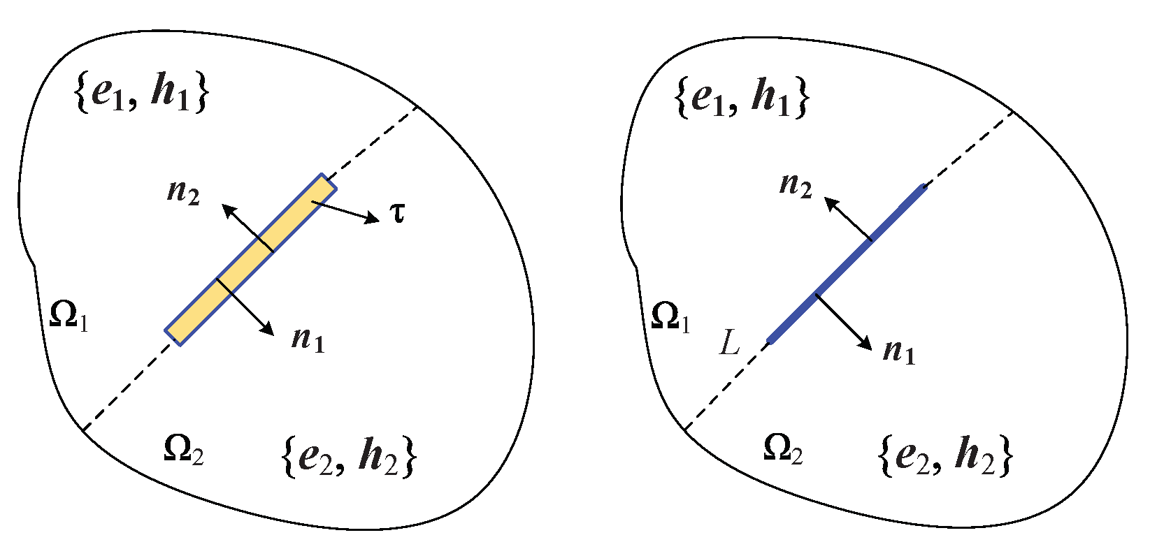
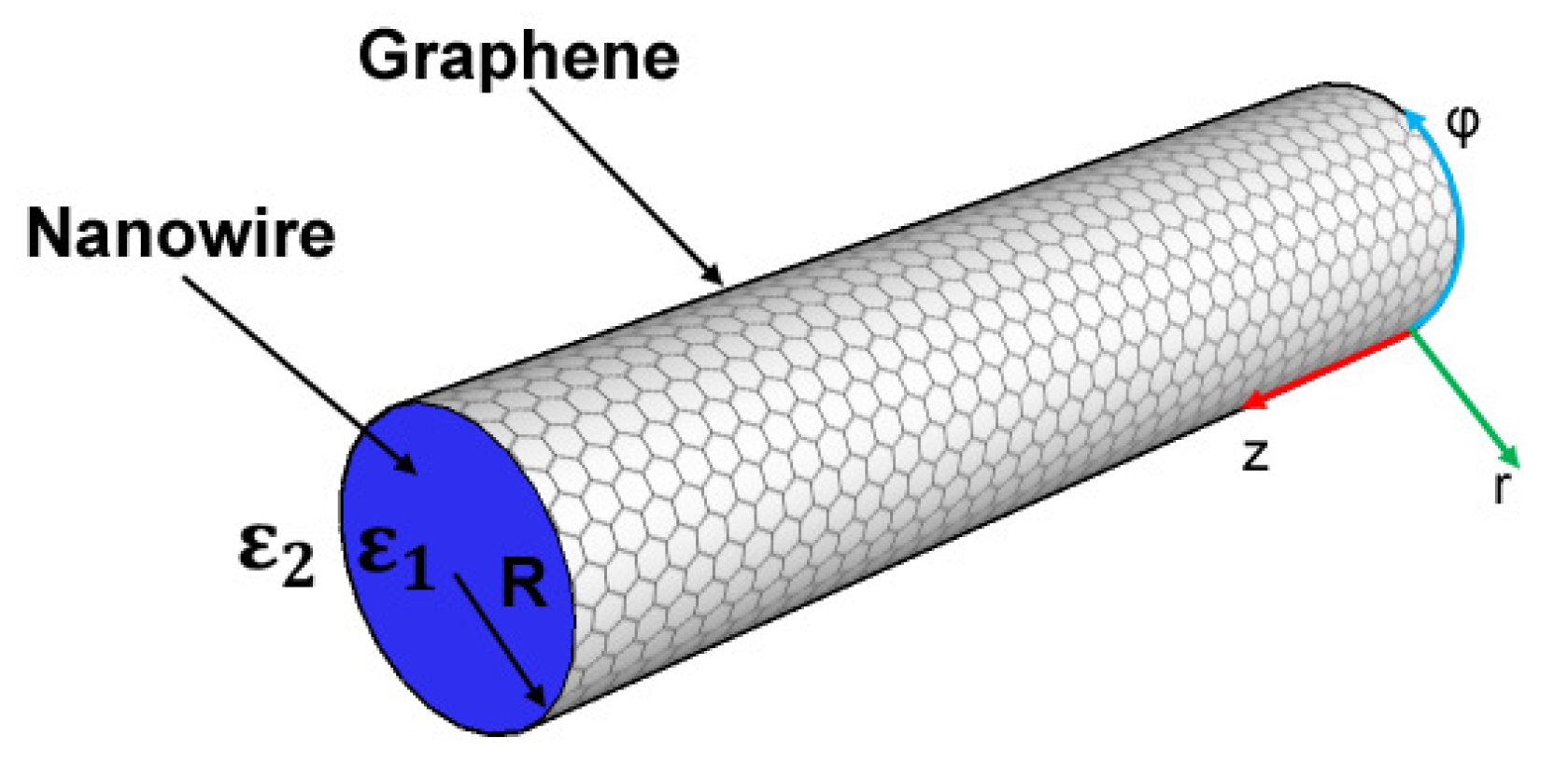
2.2.1. Impedance Transmission Boundary Condition

In the traditional FEM, due to its simplicity and feasibility, the graphene is assumed to be a layer of finite-thickness with a specific volumetric conductivity [57]. However, a graphene sheet having finite thicknesses results in exceedingly small meshes and a substantial number of unknowns when it is directly discretized. Therefore, to ensure numerical accuracy, a large amount of CPU time and memory costs are required. The impedance boundary condition (IBC) is an useful way for eliminating thin plates from the computational field, such as impedance network boundary condition (INBC), impedance transmission boundary condition (ITBC) and surface impedance boundary condition (SIBC). By using two-port network equations to describe the field inside the conductive sheet, INBC is effectively implemented in both FDTD and FEM. Meanwhile, Leontovich proposed a hypothetical SIBC for thin plates that the thickness is less than or equal to the skin depth. However, when the frequency of graphene reaches the terahertz band, the thickness of graphene is much lower than the skin depth. Therefore, ITBC is a better fit method to describe the interdependent tangential electromagnetic field on each side of graphene surface [58]. In order to clearly describe the implementation of ITBC, Figure 1 uses two triangular elements that share ITBC to illustrate.
The prerequisite for employing ITBC is that the wavelength and skin depth δ are larger than the conducting sheet’s thickness τ . As shown in Figure 2, it can be observed that using line segments to represent thin conductive sheets with finite thickness in a 2-D waveguide cross-section model [57]. The condition for using ITBC is that the wavelength and the skin depth δ are greater than the conducting sheet’s thickness τ , while avoiding sharp edges and angles. At this dot, the electromagnetic field is transmitted on either side of a sheet. Meanwhile, considering the interdependence of electromagnetic fields above and below the thin film, ITBC uses transmission line theory to represent the relationship between tangential electromagnetic fields above and below the line segment L:
n 1 × h 1 n 2 × h 2 = Y 11 Y 12 Y 12 Y 11 n 1 × n 1 × e 1 n 2 × n 2 × e 2
Graphene nanoribbon sandwich waveguide [59] is considered which placed in vacuum background, with two identical graphene ribbons on both sides and a dielectric strip with a refractive index of n d = 1.4 in the middle as shown in Figure 3 [57]. In the model, the graphene is an isotropic medium which thickness is 0.5 nm and Γ = 0.1 meV, μ c = 0.5 eV, and T = 300 K. The computational domain of 20 µm × 20 µm yields 11,212 elements, including 81,011 unknowns. Figure 4 shows the calculation results k z / k 0 for the first twelve modes. We clearly see that the solutions of mixed FEM-ITBC and FEM have good consistency. In addition to the accuracy of the mixed FEM-ITBC, Table 1 also shows that the mixed FEM-ITBC incurs lower memory costs and requires less CPU time than the traditional FEM.

2.2.2. Surface Current Boundary Condition

The previous ITBC is only applicable to model isotropic media. The modeling thin layers of anisotropic media requires the use of SCBC. In the right figure of Figure 2, one-dimensional lines are used to replace thin conductive sheets with finite thickness. When graphene thin layers are equivalent to zero thickness [39,60], fine mesh generation is avoided. SCBC is expressed as:
n × ( h 2 h 1 ) = J s = σ s e
where e is the electric field, σ s is the surface conductivity of the nanomaterial sheet which is anisotropic media. n = n 1 = n 2 is the unit normal vector from Ω 1 to region 2. h 1 , h 2 are the magnetic fields of Ω 1 and Ω 2 , respectively.
Figure 5 shows a graphene-coated dielectric nanowire waveguide (GNW), with an inner layer of dielectric nanowires and an outer layer covered with graphene sheet. The nanowire with a radius of R = 100 nm has a relative permittivity of ε r 1 = 3 and the external region has a relative permittivity of ε r 2 = 1 . The surface conductivity s of graphene σ s is calculated using Kubo’s formula with μ c = 0.5 eV, T = 300 K, and τ = 200 ns. A PML which thickness is 0.5 µm is utilized to truncate the open GNW structure. The length and width of the calculation area are both 5 µm. Through comparing the results calculated by the mixed FEM-SCBC method with the analysis results [61], the field distributions of the first three propagation modes (m0, m1, m2), propagation lengths L = 1 / [ 2 Im ( k z ) ] , and the dispersion relations as a function of frequency is investigated. The proposed method has been proven to be accurate, as presented in Figure 6a,b, with maximum relative errors of 0.4% and 0.15%, respectively. The field distributions of the modes (m0, m1, m2) in Figure 6c are also in well-alignment with the field distribution of the analytical method. Furthermore, Table 2 demonstrates that the mixed FEM-SCBC is a more valuable option to studying the propagation characteristics of plasmonic waveguides which is based on graphene, as it requires only 91,997 DoFs and avoids the demand for a dense mesh around the graphene. In contrast, the traditional FEM requires 384,737 DoFs to discretize thin graphene sheets with a thickness of 0.5 nm. In summary, this method offers both effectiveness and computational efficiency for the analysis of graphene-based plasmonic waveguides. The results in [62] show that the experimental results are in good agreement with the numerical results, which proves the effectiveness of the numerical method of replacing graphene with SCBC.

2.3. Mixed Spectral Element Method with SCBC

The SEM which combines spectral method with FEM extended by Patera. Due to its unique basis function construction method and node arrangement, it achieves higher accuracy than the FEM, and consumes less memory costs and computational time. For solving Stokes equations in fluid mechanics, Patera took the lead in introducing spectral methods into calculations, resulting in better numerical accuracy and convergence compared to traditional methods [64]. Since then, the SEM has been widely used in numerical calculations simulation in the field of fluids. Later, pseudospectral method was proposed by Chebyshev, and Liu incorporated the pseudospectral method into the FEM [65]. The SEM has become a new and efficient tool for electromagnetic numerical computation.
The mixed SEM possesses both spectral accuracy and the capability to eliminate zero spurious eigenvalues [66]. The combination of SCBC and mixed SEM is utilized to analyze the modes of graphene based pasmonic waveguides due to their enormous potential in eigenvalue solver. This method employs a new variational formulation to suppress zero spurious modes by introducing Gauss’ law to the vectorial Helmholtz equation. Additionally, an equivalent SCBC is used in the computational domain to replace the nanoscale graphene sheets.
A tunable multilayer nanoring waveguide consisting of six layers of graphene and seven layers of dielectric is firstly considered. The graphene and dielectric layers are alternately distributed [67]. Figure 7 depicts the cross-section and three-dimensional structure of the waveguide. The innermost ring radius is 140 nm, and the total ring radius is 210 nm. The innermost and outermost layers have a thickness of 10 nm, while the rest layers and graphene sheets are 9.5 nm and 0.5 nm thick, respectively. The dielectric layer has a relative permittivity of 2.1. In this situation, the environment temperature is T = 300 , τ = 0.5 ps and μ c = 0.5 eV. The relative dielectric constant of graphene is expressed as ε r = 2.5 j σ s / ( ε 0 ω d ) [40], where d represents the thickness of graphene.
The multilayer nanoring open waveguide is truncated using a PML with 100 nm thickness, and the entire computational domain size was 1.2 µm × 1.2 µm. To obtain accurate simulation results for the graphene sheets, traditional FEM requires a dense finite element mesh with 127,620 triangular elements, yielding 893,421 unknowns. Instead, the mixed SEM-SCBC method substitutes SCBC for graphene sheets in the computational domain. As a result, only 1449 quadrilateral elements are produced across the entire domain, and only 17,528 of them are unknown. Figure 8a displays the extremely fine meshes of graphene sheet, where at least one element is discretized in the graphene sheet, while Figure 8b displays the quadrilateral elements that result from SCBC, which are relatively coarse. It is evident that using SCBC instead of graphene sheet significantly decrease on the number of elements and degrees of freedom (DOFs) required for numerical calculations.
The mixed SEM-SCBC is employed to simulate the numerical dispersion relationship of graphene waveguides. Figure 9 shows the relationship between the real part of the effective refractive index (Real( N eff ) , N eff = k z / k 0 ) and the operating frequency. When m = 0 is a fixed, the real part of the effective refractive index varies with n, with mode ( 0 , 1 ) being the lowest among modes ( 0 , n ) . The propagation lengths, represented by L p = λ 0 / 4 π [ Im ( N eff ) ] in Figure 10, are calculated based on the operating frequency. It can be observed that higher order modes experience more losses compared to lower order modes, which is in line with the characteristics of propagation modes. In this figure, the numerical results of traditional FEM are presented by –, – –, and · lines. The proposed mixed SEM-SCBC method has great consistency with the traditional FEM with graphene sheet, but with significantly lower CPU time and memory costs (only 3% and 2%, respectively), as shown in Table 3. These results demonstrate that the mixed SEM-SCBC can enhance computing speed and save computer resources.

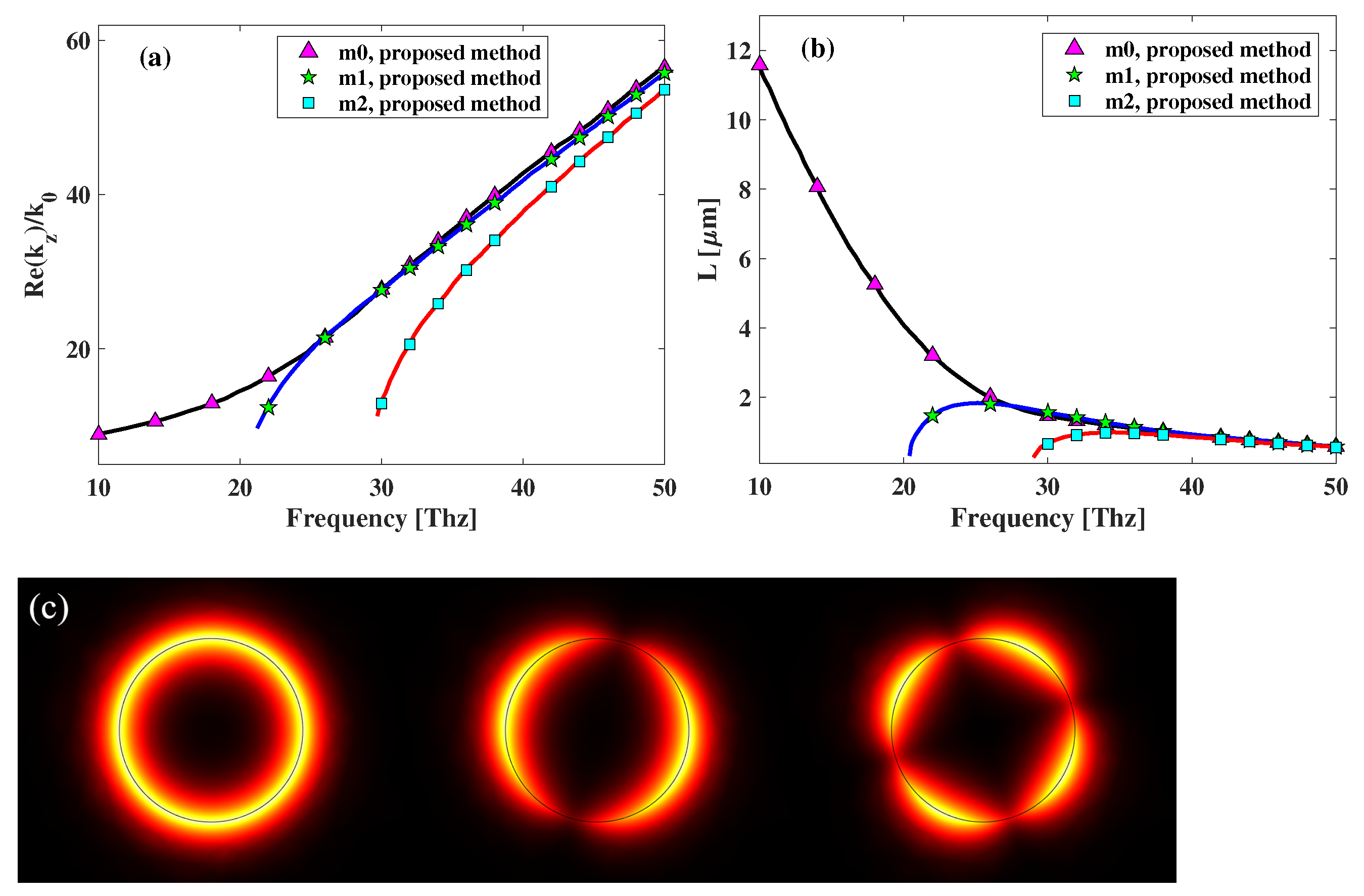
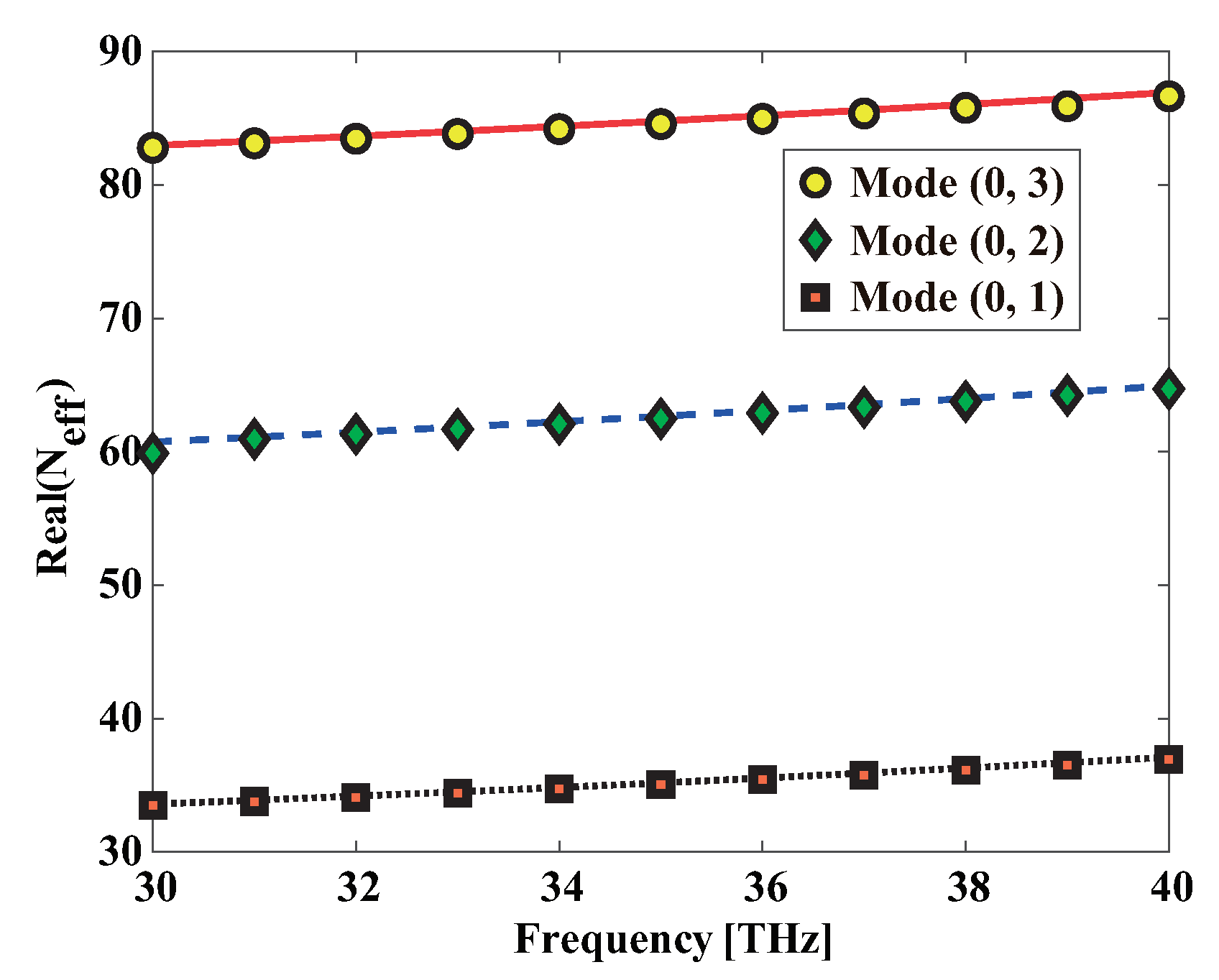
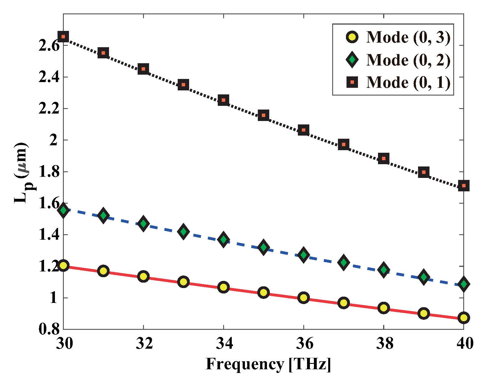
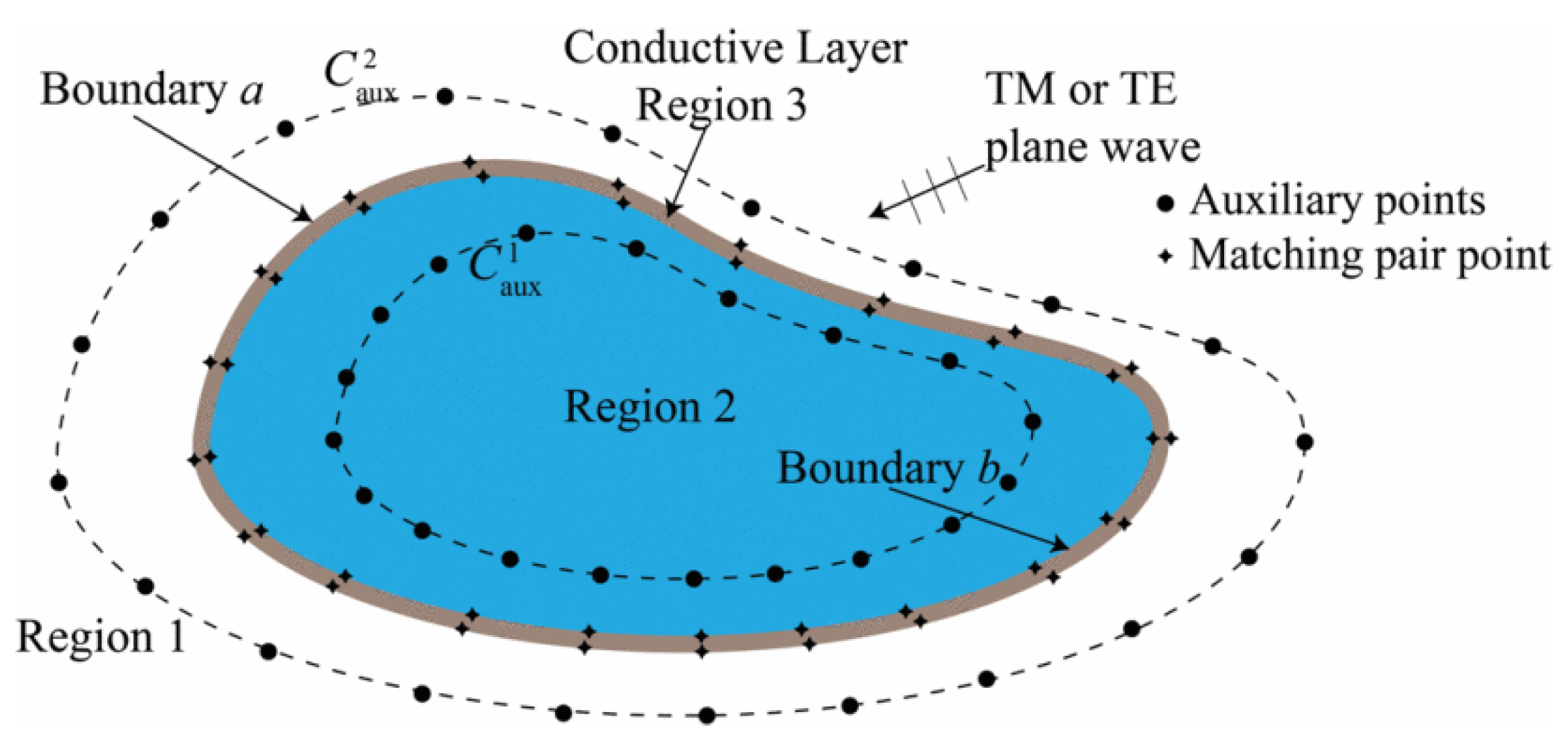
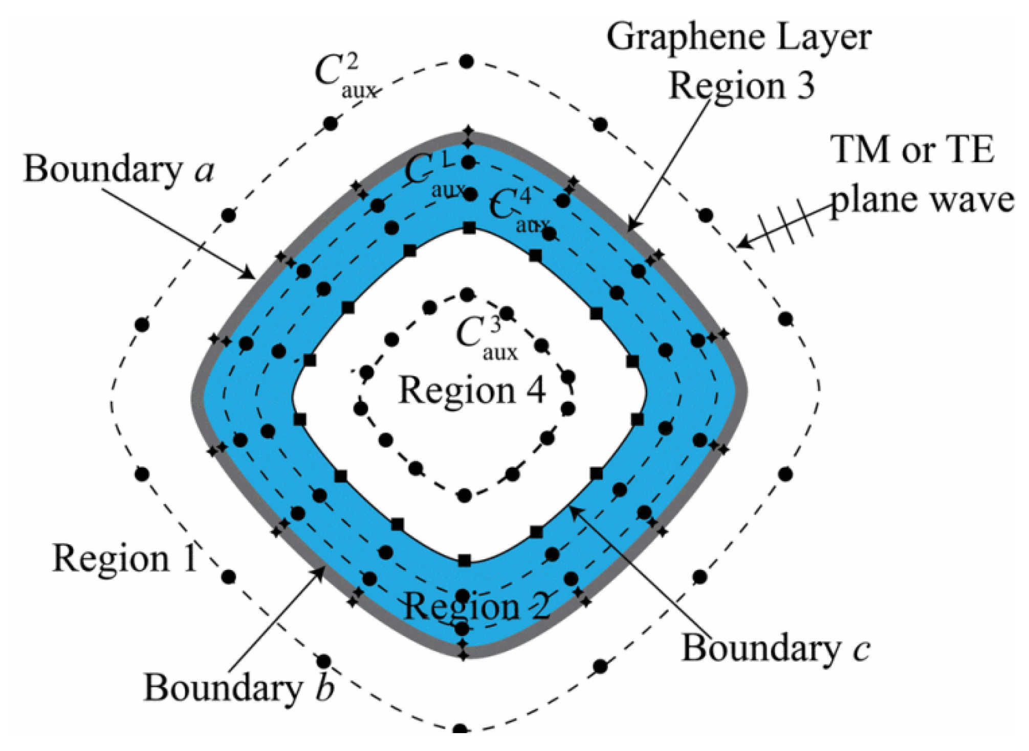
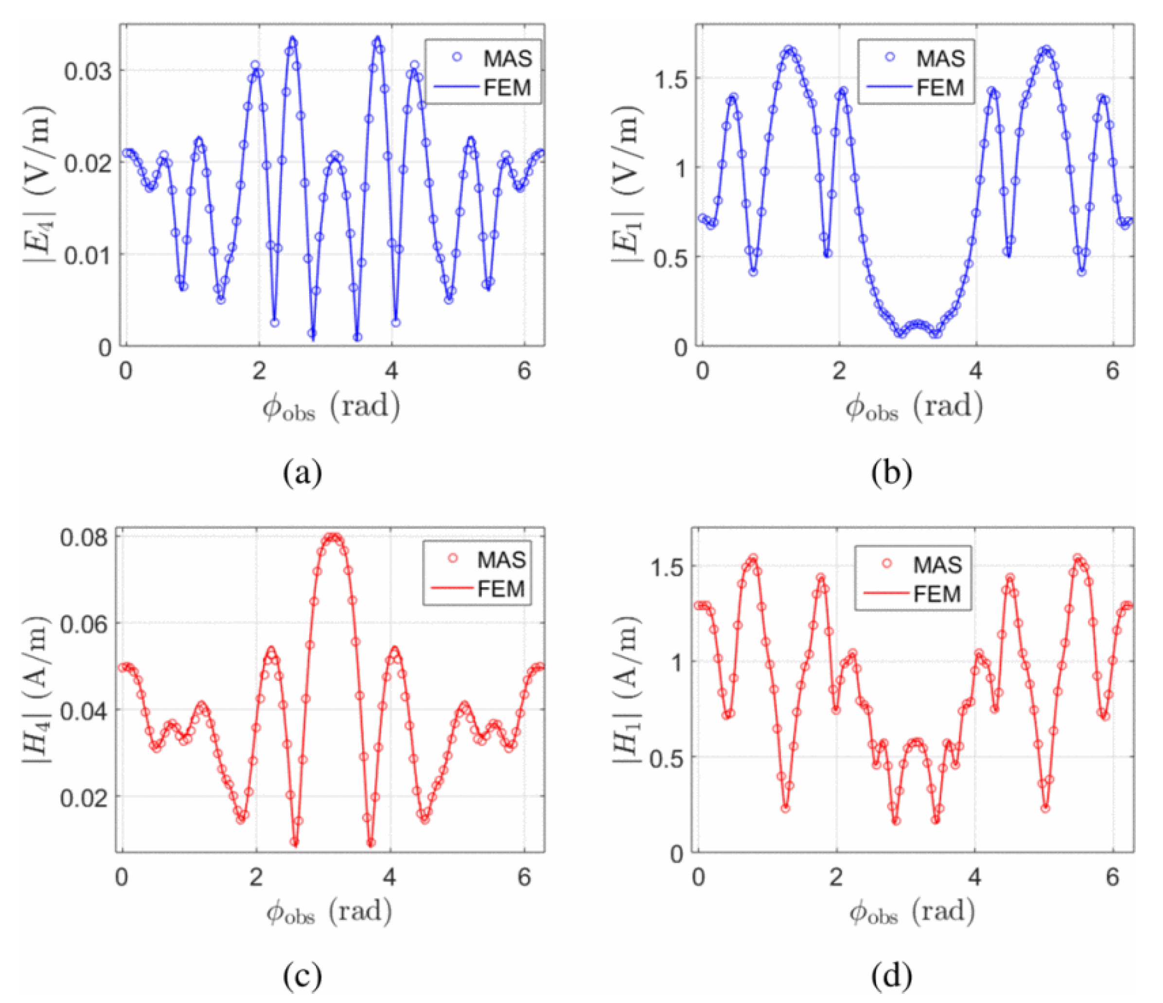
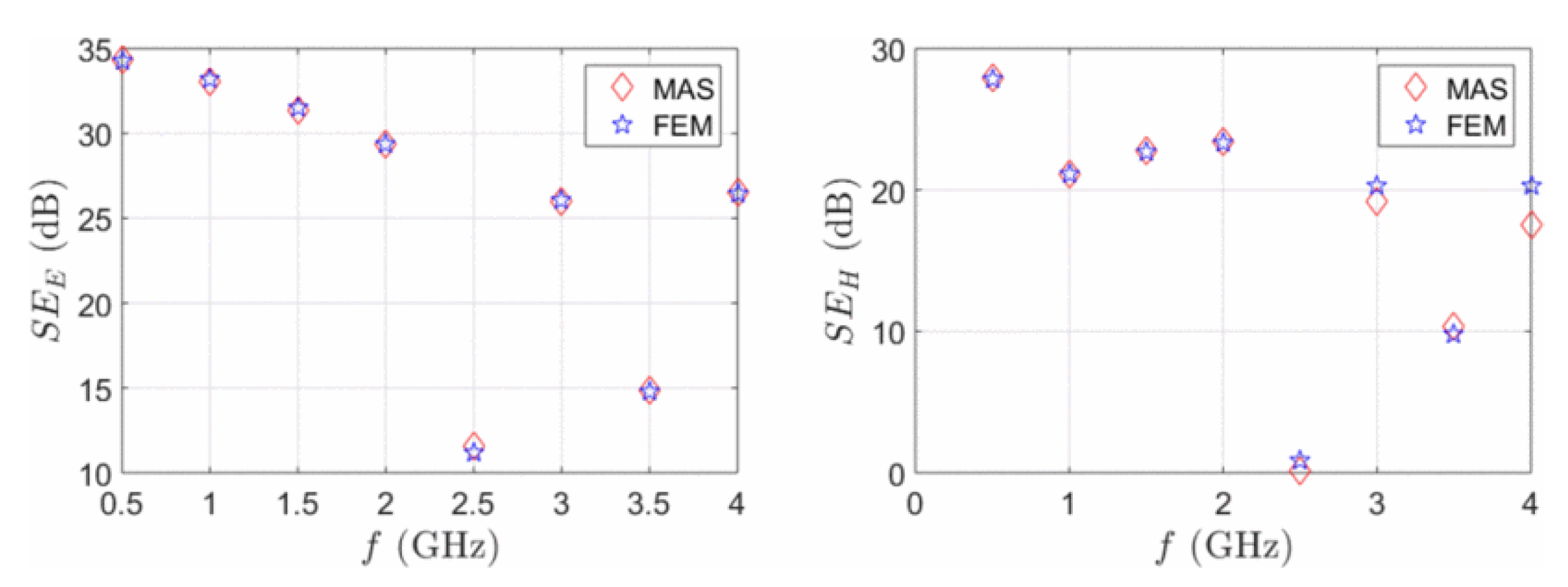
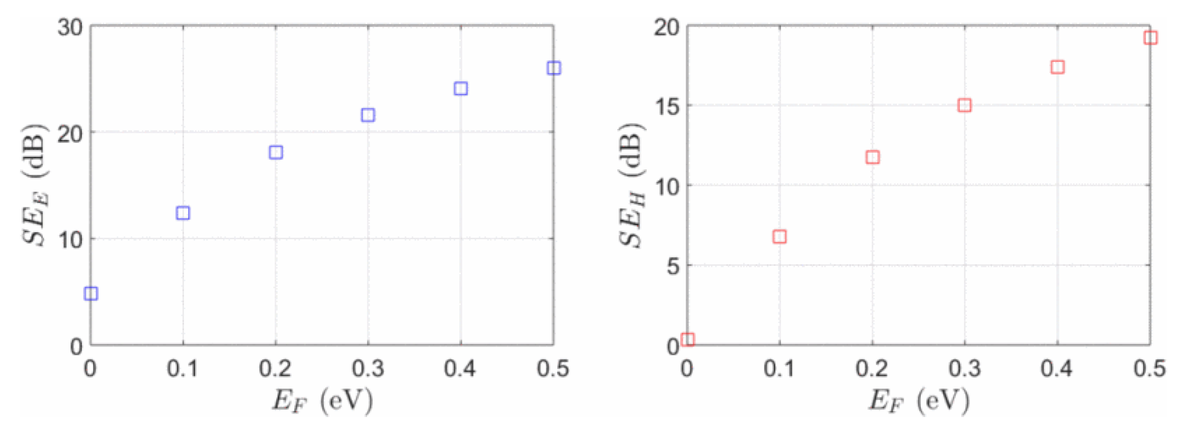
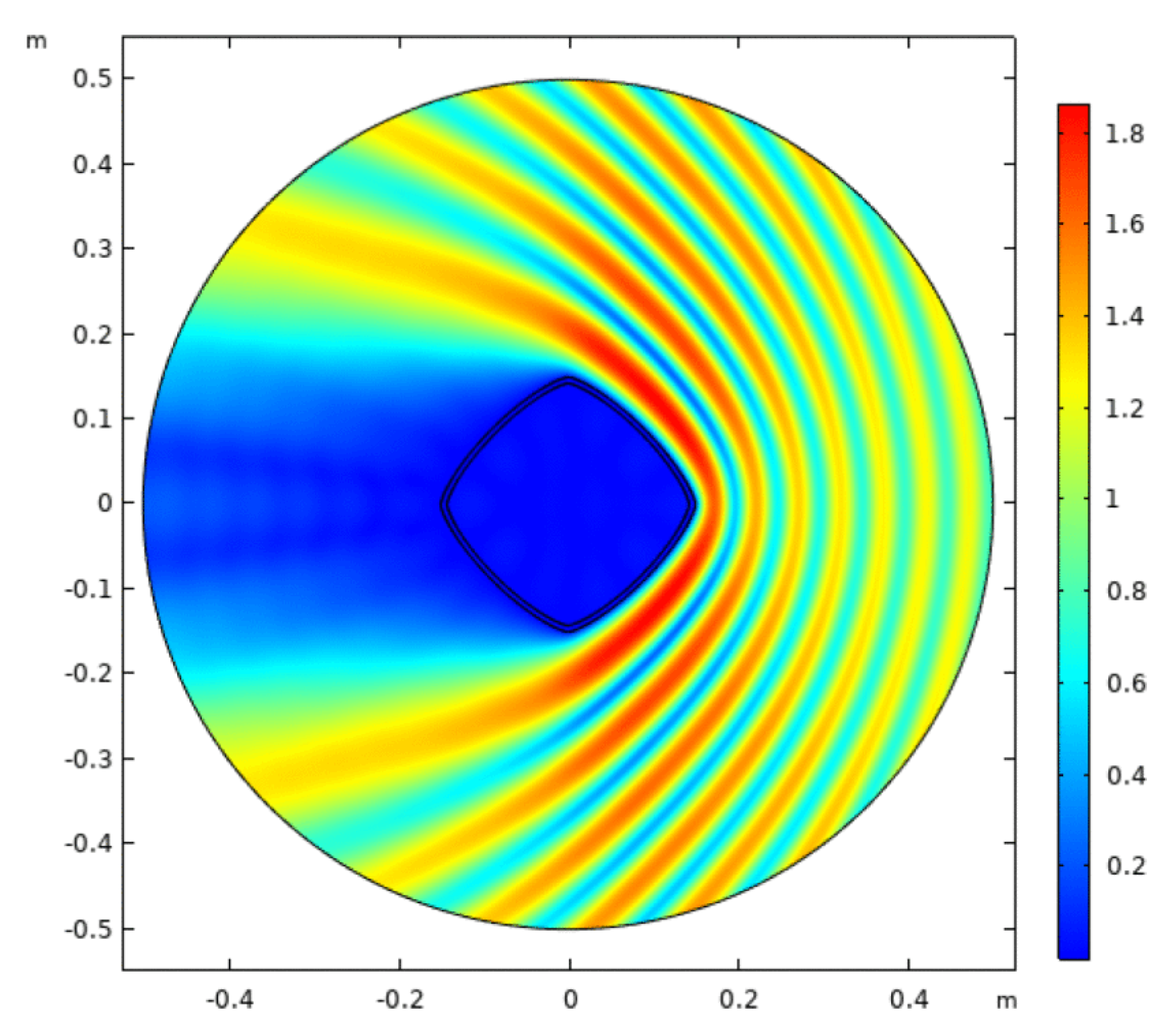
2.4. The Method of Auxiliary Sources with IMBC

The electromagnetic waves are incident on a conductive layer that separates the layered medium in a normal shielding configuration. The conductive layer can block the incident field and act as an electromagnetic shield. The planar, cylindrical, and spherical interfaces are the most common layered media models used to demonstrate electromagnetic shielding. However, for the high conductivity of interior materials, the conventional MAS [69,70] approach yields divergent results. In Figure 11, if the standard MAS described in [71,72] is used to calculate the shielding effect, a convergent field cannot be obtained within the highly conductive layer. Therefor, a modified version of MAS was proposed in [73] to improve by associating the field at each point of boundary a with the electric field at the corresponding point of boundary b. This effect can be achieved by replacing the conductive layer with the IMBC. The shielding effectiveness of a single layer of graphene covering a cylindrical structure can be calculated using this modified method.
By superposing the fields emitted by N 1 and N 2 filaments set on the auxiliary surfaces C a u x 1 and C a u x 2 , it is possible to replicate the internal field in region 2 and the scattering field in region 1. The N 1 and N 2 filaments, which radiate in the dielectric-filled unbounded space of regions 1 and 2, respectively, and carry unknown currents I 1 l ( K 1 l ) , l = 0 , , N 1 1 and I 2 l ( K 2 l ) , l = 0 , , N 2 1 , respectively. The field of the l-th source produced in region m ( m = 1 , 2 ) is expressed as:
E m l ( x , y ) = z ^ k m Z m 4 I m l H 0 ( 2 ) ( k m ρ m l )
H m l ( x , y ) = k m 4 i I m l x ^ ( y m l y ) + y ^ ( x x m l ) ρ m l × H 1 ( 2 ) ( k m ρ m l )
for the TM z case, and
H m l ( x , y ) = z ^ k m 4 Z m K m l H 0 ( 2 ) ( k m ρ m l )
E m l ( x , y ) = k m 4 i K m l x ^ ( y m l y ) + y ^ ( x x m l ) ρ m l × H 1 ( 2 ) ( k m ρ m l )
for TE z polarization, where ( x m l , y m l ) denotes filament coordinates in region m, ρ m l denotes the separation between the observation point ( x , y ) and the l-th filament in region m, I m l and K m l denote the current and magnetic current amplitudes of the l-th filament in region m, k m = ω μ m / ε m and Z m = μ m / ε m denote the wave number and impedance of region m, respectively.
Then, the 2-D-IMBC approach is applied to M matching pairs. This is done to associate the fields at specific points on boundary a with the fields at corresponding points on boundary b.
n ^ a × ( n ^ a × E a ) n ^ b × ( n ^ b × E b ) = Z S r b r a Z t r r a r b Z t r Z S n ^ a × H a n ^ b × H b
where Z t r = i Z 3 csc ( k 3 ) and Z s = i Z 3 cot ( k 3 ) are the transfer and surface impedance, k 3 and Z 3 denote the wavenumber and characteristic impedances of the conductive layer, the curvature radii on boundaries a and bare r a and r b , respectively. The appendix of [75] shows that n ^ a = n ^ = n ^ b and r a = + r b for uniformly thick conductive layers.
Figure 12 studies a multi-layer cylindrical medium with a circular square cross-section. Wherein region 3 is a graphene monolayer, region 2 is a silicon dioxide (SiO2) layer, air is filled in both regions 1 and 4; thus, ε 1 = ε 4 = ε 0 and ε 2 = 3.9 ε 0 . The surface conductivity of graphene with E F = 0.5 eV, τ = 6.582 ps, T = 300 K and = 0.5 nm is utilized. Boundary b has collocation points with the following coordinates:
x b = 15 sgn ( cos θ ) | cos θ | 3 2 y b = 15 sgn ( sin θ ) | sin θ | 3 2
A TMz or TEz plane wave incident the computational domain. There are four sets of auxiliary sources N 1 = N 2 = N 3 = N 4 = 110 , each placed on coordinate sources ( x a _ 1 , y a _ 1 ) = 0.8 ( x b , y b ) , ( x a _ 2 , y a _ 2 ) = 2 ( x b , y b ) , ( x a _ 3 , y a _ 3 ) = 0.8 ( x c , y c ) and ( x a _ 4 , y a _ 4 ) = 1.2 ( x c , y c ) of C a u x 1 , C a u x 2 , C a u x 3 , and C a u x 4 . Applying the boundary condition Equation (10) to a and b on the M = 110 matching pair. The norm of the fields in regions 1 and 4 with ( x o _ 1 , y o _ 1 ) = 2 ( x b , y b ) and ( x o _ 2 , y o _ 2 ) = 0.6 ( x c , y c ) are described in Figure 13. It is also shown that the modified MAS in good agreement with the finite element calculation results of COMSOL. The relationship between the shielding effect with E F = 0.5 and f, and the relationship between the shielding effect with f = 3 GHz and E F are presented in Figure 14 and Figure 15, respectively. The modified MAS not only matches the finite element calculation results, but also has advantages in memory usage. The shielding effect is shown in Figure 16.

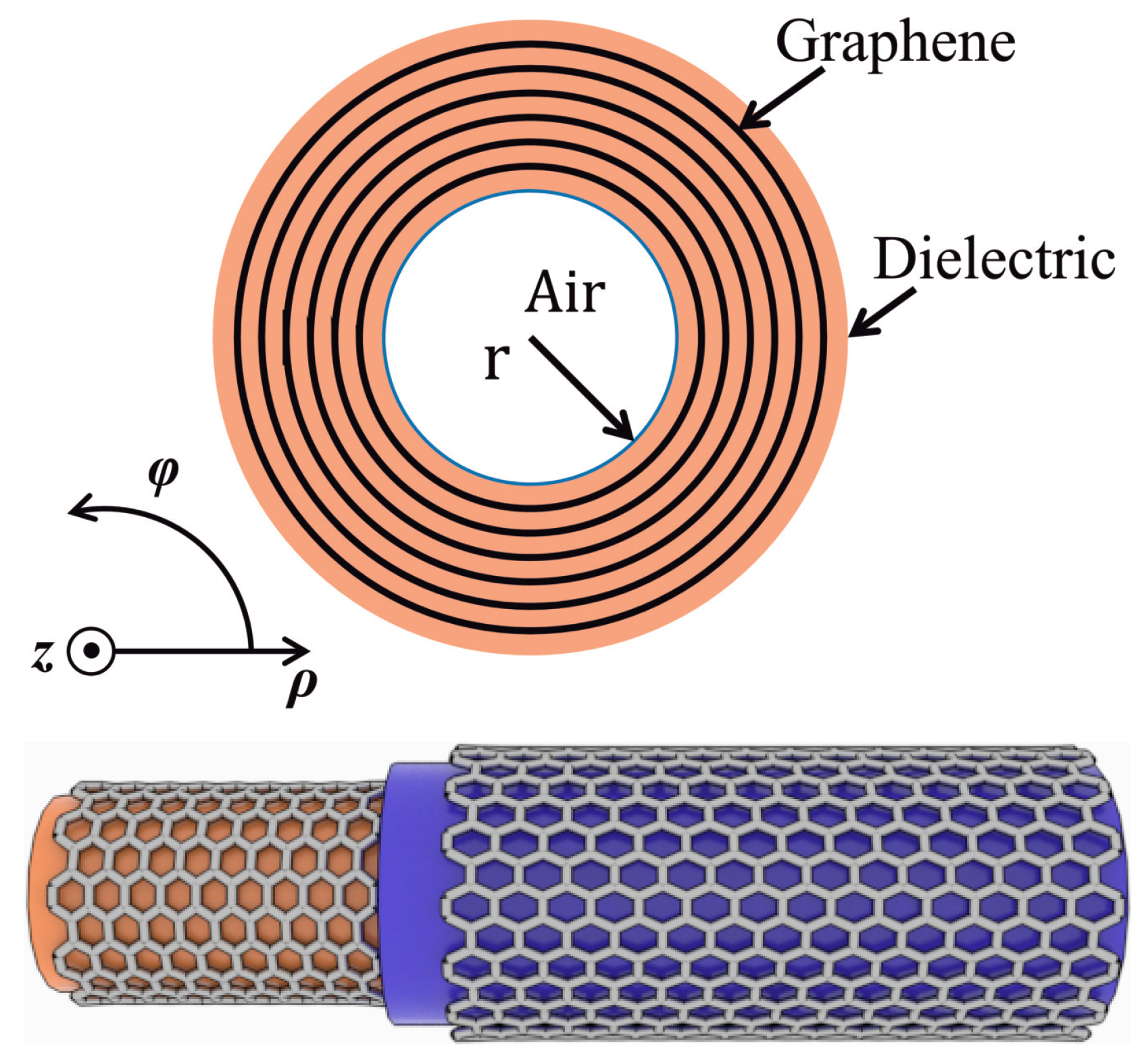
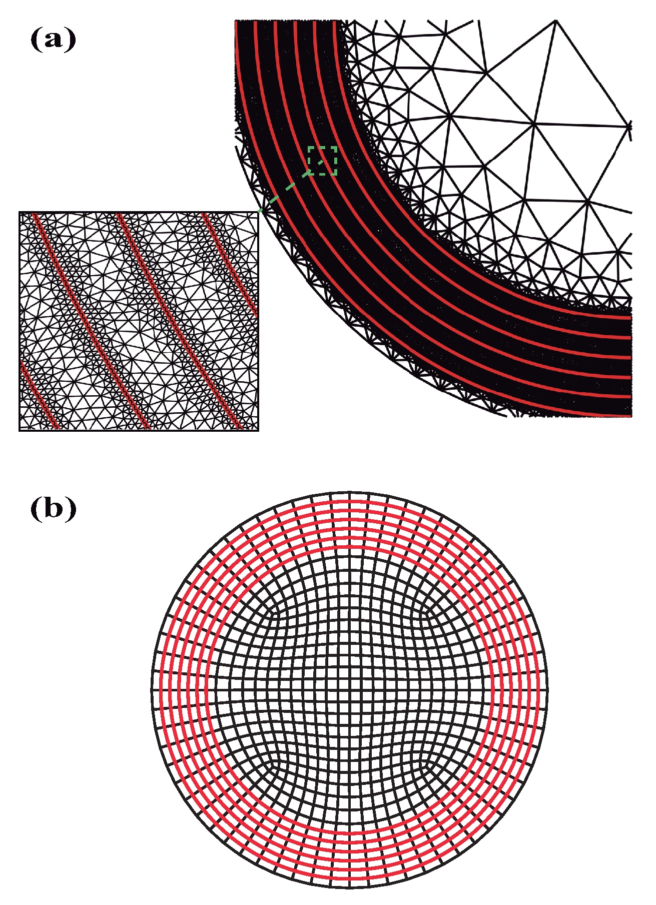
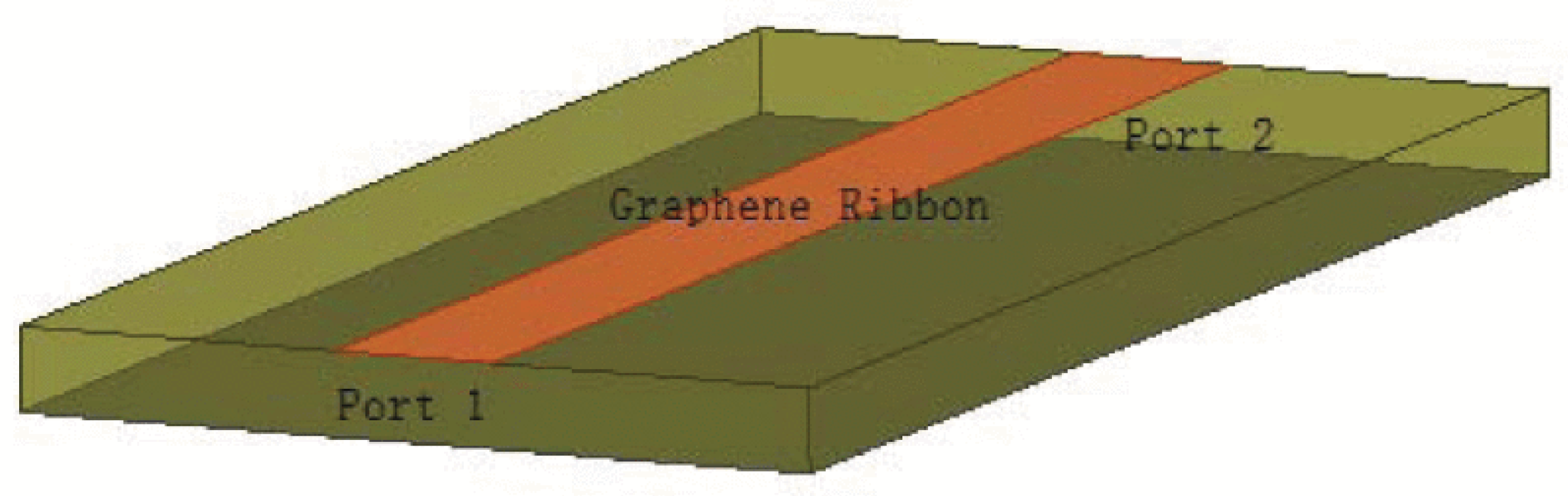
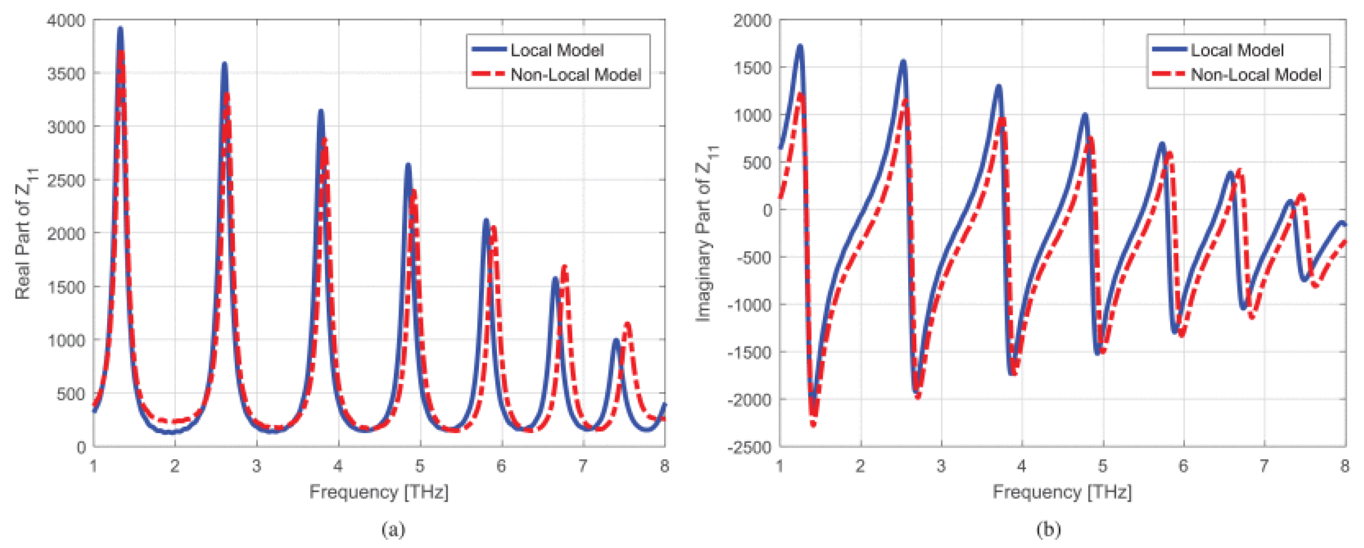
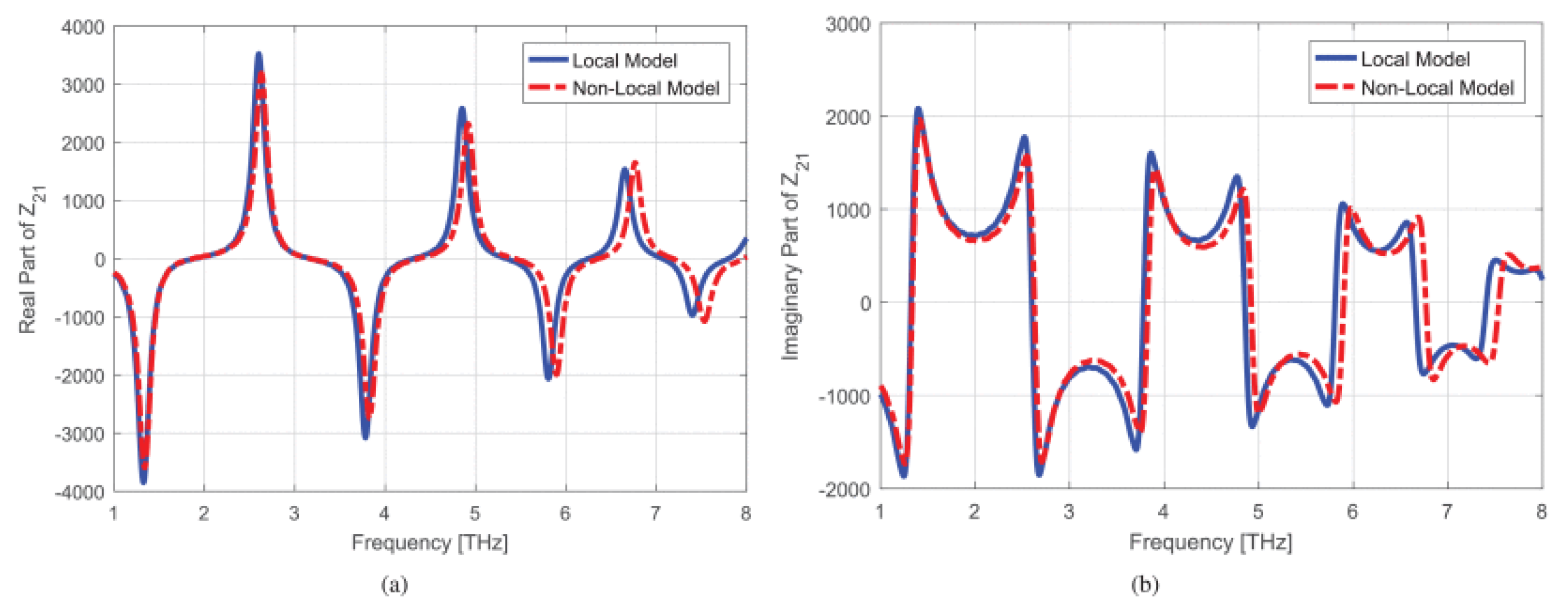
2.5. Discontinuous Galerkin Time-Domain Method with SIBC

The DGTD method is a versatile approach for solving differential equations in numerous fields such as computational science, engineering, and physics. It incorporates the advantages of the finite volume method (FVM) [76,77] and the FEM, enabling mesh discretization of the computational domain. The spatial DGTD operations, like FVM, are localized, and the global mass matrix is transformed and divided into a block diagonal mass matrix. The inversion and storage of the mass matrix block [78] are performed before initiating time marching. This makes the solver of DGTD very compact, especially when using explicit integration methods. These characteristics make DGTD an excellent method for simulating multi-scale electromagnetic fields in two-dimensional materials.
Since the jumping depth of graphene is much greater than the thickness of the graphene layer, the SIBC is utilized to replace the graphene layer, which is expressed as:
n ^ × ( E 2 E 1 ) = 0 σ g 1 · [ n ^ × ( H 2 H 1 ) ] = σ g 1 · J = E
where E 1 and E 2 indicate the total electric field intensity on each side of the graphene layer, respectively. H 1 and H 2 represent the total magnetic field intensity on each side of the graphene layer, respectively. n ^ indicates the unit normal vector above the graphene layer, pointing outwards from the plane. J is the induced polarization current density in the graphene layer and E represents the intensity of the electric field. Due to the assumption that σ g is usually independent of the spectral wavenumber, only spatially localizatied model needs to be considered. However, when the graphene ribbon is in the nanometer scale, the electromagnetic field is related to the field at current position and the role of the field in surrounding environment, therefor σ g is the spatially dispersive, i.e., the nonlocal conductivity [28,79]. The nonlocal conductivity of graphene nanoribbon needs to be considered, which is shown in [80].
A graphene nano-ribbon transmission line is simulated and the electromagnetic field interaction on graphene nano-ribbon (GNR) located on silicon substrate is analyzed. As is shown in Figure 17, the GNR dimension is 0.3 µm × 3 µm × 0.05 µm. Port 1 is the current source, and both non-local and local conductivity models are simulated. Time-voltage is recorded at ports 1 and 2 of the nanobelt transmission line in two simulation models (see Figure 18). Figure 19 and Figure 20 show the relationship between Z 11 and Z 21 with frequency. Results in the time domain differ significantly from those in the frequency domain, especially in the high-end terahertz band which indicate the importance of the nonlocal conductivity of graphene.

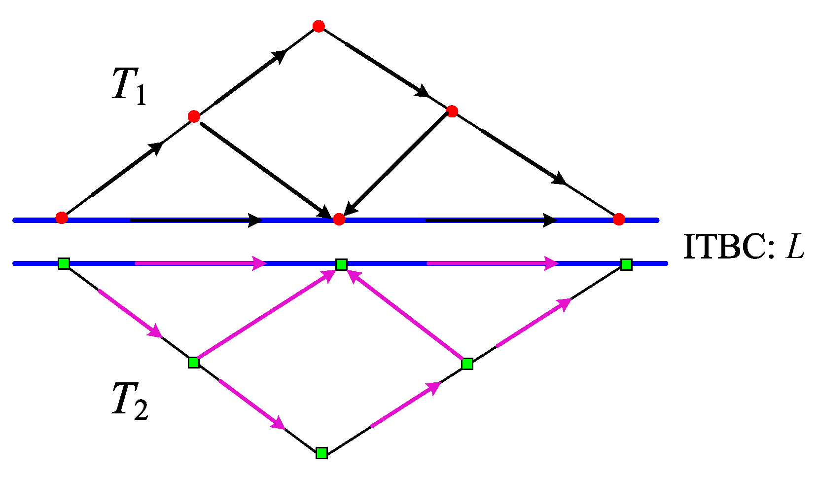
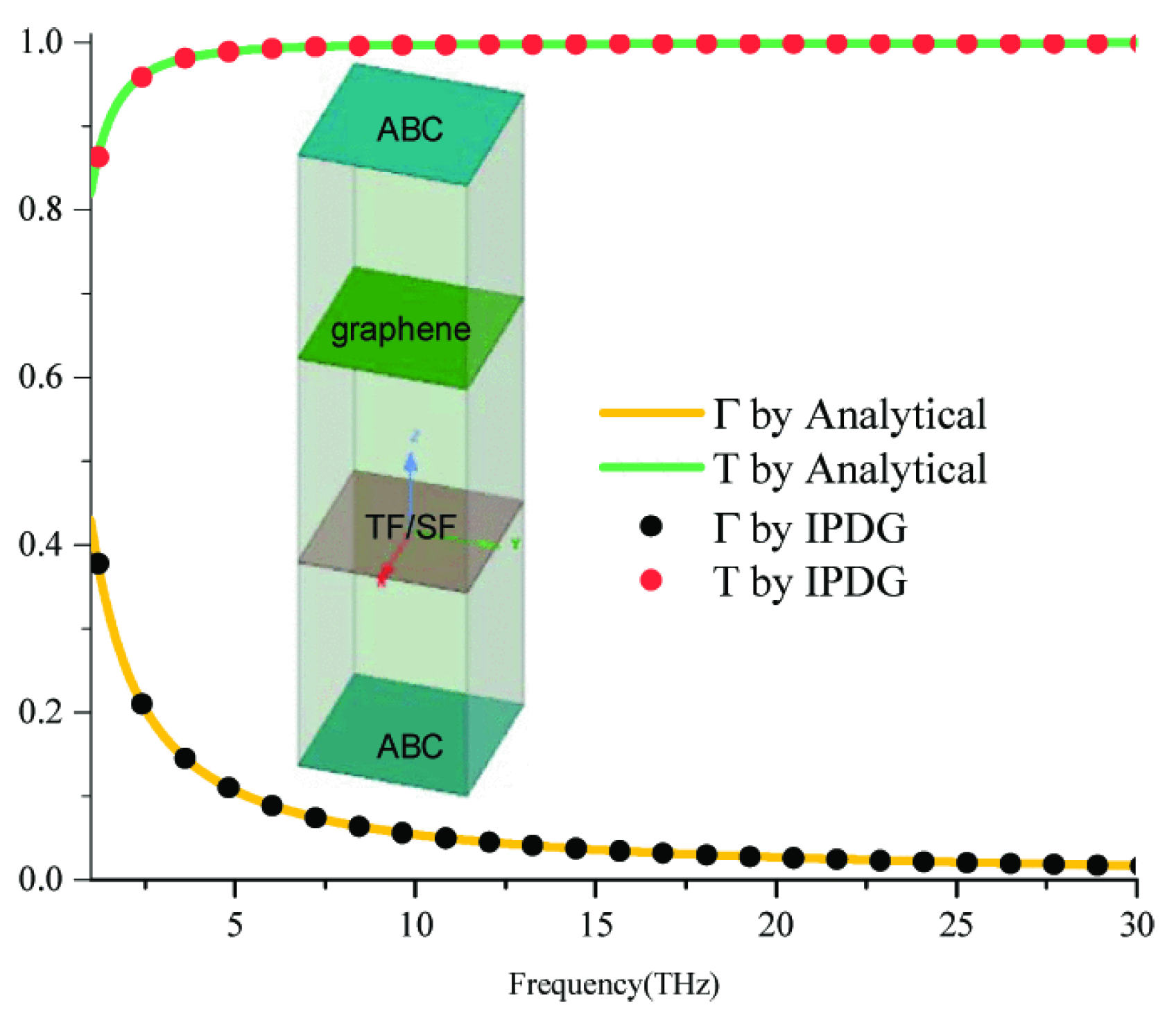
2.6. Interior Penalty Discontinuous Galerkin-Time Domain Method with ITBC

The IPDG, a DG method, is also a good method for solving electromagnetic problems, including modeling graphene as an infinitely thin impedance surface using ITBC [81], which minimizes memory usage and computation time.
Equation (1) expresses the surface conductivity as a frequency-domain expression, which is difficult to solve in time domain. To overcome this, the vector-fitting technique [82] is employed to approximate σ g as the sum of partial fractions of the extreme residual pairs, either in the form of real or complex conjugate, on the frequency band. Equation (1) is modified as:
σ g = l = 1 N σ l = l = 1 N r l j ω p l
where N is the total number of poles and p l and r l are residuals and poles, respectively. Assuming a computational domain Grammar which has boundary Γ b . The entire computational domain is discretized into multiple non-overlapping tetrahedrons, with Γ i n t e r i o r representing all inner surfaces and Γ I T B C representing the inner surfaces attached to the graphene surface. The enhanced IPDG method using ITBC is reformulated as:
Ω ε 2 E ˜ t 2 · N i d r + Ω μ 1 × E ˜ · × N i d r Γ I T B C J S · N i d S Γ i n t e r i o r E ˜ * E ˜ · μ 1 × N i T d S Γ i n t e r i o r ( μ 1 × E ˜ ) * · N i T d S + Γ i n t e r i o r E ˜ * E ˜ T · μ 1 × N i d S + Γ i n t e r i o r ( μ 1 × E ˜ ) * T · N i d S + Γ b n × ( μ 1 × E ˜ ) * · N i d S + Γ b n × ( E ˜ * E ˜ ) · μ 1 × N i d S = 0
where n indicates the unit vector, which points towards the graphene sheet. E ˜ = t 1 E is expanded with vector basis function N i . · T represents tangential jump, · represents the average value on the face f of an element, and the superscript “*” represents numerical flux.
Assuming an infinite graphene sheet, the x direction boundary is taken as PEC while PMC is considered as the boundary in the y direction. The truncated boundary is a first-order ABC in the z direction. The entire domain size is 10.5 µm ×   2.5 µm ×   2.5 µm, and a plane wave source is created using total/scattered field boundary conditions. Unfolding unknown fields using full two vector basis functions, with a time step size of t is 5 e 17 s. The graphene parameter μ c is estimated to be 0.15 eV. Figure 21 shows that IPDG is in good agreement with the analytical solutions.

3. Conclusions

In the past decade, due to its excellent optical properties, thermal, mechanical and electrical, widespread attention has been attracted on graphene, papers on the physical mechanisms and applications of graphene in various fields have been constantly updated. In this work, we reviewed some of the most commonly used algorithms for simulating graphene in the CEM field. The mixed FEM-ITBC and mixed FEM-SCBC and mixed SEM-SCBC are employed to solve the graphene-based plasmonic waveguide problem. The improved auxiliary source method with IMBC is used to calculate the shielding effect, which obtains a convergence field in a high conductive layer; The DGTD method with SIBC is also an effective method for exploring the spatial dispersion characteristics of graphene. The IPDG-ITBC to model graphene, saving memory and usage time. All these equivalent boundary conditions have been proposed and significantly saved computational time and memory costs. With all of these performances and improvements, we anticipate that equivalent boundary conditions are promising techniques to simulate electromagnetic response of graphene.

Author Contributions

Conceptualization, N.L. and Y.G.; methodology, N.L. and Y.G.; software, N.L. and Y.G.; investigation, N.L. and Y.G.; resources, N.L. and Y.G.; writing—original draft preparation, Y.G.; writing—review and editing, N.L. and Y.G.; visualization, N.L. and Y.G.; supervision, N.L. and Y.G.; project administration, N.L. All authors have read and agreed to the published version of the manuscript.

Funding

The work was supported by National Natural Science Foundation of China under Grant (62271429); Opening Project of Science and Technology on Reliability Physics and Application Technology of Electronic Component Laboratory under Grant (ZHD202107-008(135)).

Institutional Review Board Statement

Not applicable.

Informed Consent Statement

Not applicable.

Data Availability Statement

The data represented in this study are available on request from the corresponding author.

Conflicts of Interest

The authors declare no conflict of interest.

Abbreviations

Mixed FEMMixed Finite Element Method
Mixed SEMMixed Spectral Element Method
MASMethod of Auxiliary Sources
DGTDDiscontinuous Galerkin Time-domain
IPDGInterior Penalty Discontinuous Galerkin
ITBCImpedance Transmission Boundary Condition
SCBCSurface Current Boundary Condition
IMBCImpedance Matrix Boundary Condition
SIBCSurface Impedance Boundary Condition

References

  1. Novoselov, K.S.; Geim, A.K.; Morozov, S.V.; Jiang, D.E.; Zhang, Y.; Dubonos, S.V.; Grigorieva, I.V.; Firsov, A.A. Electric field effect in atomically thin carbon films. Science 2004, 306, 666–669. [Google Scholar] [CrossRef] [Green Version]
  2. Novoselov, K.S.; Fal’ ko, V.I.; Colombo, L.; Gellert, P.R.; Schwab, M.G.; Kim, K. A roadmap for graphene. Nature 2012, 490, 192–200. [Google Scholar] [CrossRef] [PubMed]
  3. Geim, A.K.; Novoselov, K.S. The rise of graphene. Nat. Mater. 2007, 6, 183–191. [Google Scholar] [CrossRef] [PubMed]
  4. Lai, R.; Shi, P.; Yi, Z.; Li, H.; Yi, Y. Triple-Band Surface Plasmon Resonance Metamaterial Absorber Based on Open-Ended Prohibited Sign Type Monolayer Graphene. Micromachines 2023, 14, 953. [Google Scholar] [CrossRef]
  5. Tang, B.; Jia, Z.; Huang, L.; Su, J.; Jiang, C. Polarization-Controlled Dynamically Tunable Electromagnetically Induced Transparency-Like Effect Based on Graphene Metasurfaces. IEEE J. Sel. Top. Quantum Electron. 2021, 27, 4700406. [Google Scholar] [CrossRef]
  6. Neto, A.C.; Guinea, F.; Peres, N.M.; Novoselov, K.S.; Geim, A.K. The electronic properties of graphene. Rev. Mod. Phys. 2009, 81, 109. [Google Scholar] [CrossRef] [Green Version]
  7. Bonaccorso, F.; Sun, Z.; Hasan, T.; Ferrari, A.C. Graphene photonics and optoelectronics. Nat. Photonics 2010, 4, 611–622. [Google Scholar] [CrossRef] [Green Version]
  8. Blake, P.; Brimicombe, P.D.; Nair, R.R.; Booth, T.J.; Jiang, D.; Schedin, F.; Ponomarenko, L.A.; Morozov, S.V.; Gleeson, H.F.; Hill, E.W.; et al. Graphene-based liquid crystal device. Nano Lett. 2008, 8, 1704–1708. [Google Scholar] [CrossRef] [Green Version]
  9. Meric, I.; Han, M.Y.; Young, A.F.; Ozyilmaz, B.; Kim, P.; Shepard, K.L. Current saturation in zero-bandgap, top-gated graphene field-effect transistors. Nat. Nanotechnol. 2008, 3, 654–659. [Google Scholar] [CrossRef]
  10. Shih, C.J.; Wang, Q.H.; Son, Y.; Jin, Z.; Blankschtein, D.; Strano, M.S. Tuning on–off current ratio and field-effect mobility in a MoS2–graphene heterostructure via Schottky barrier modulation. ACS Nano 2014, 8, 5790–5798. [Google Scholar] [CrossRef]
  11. Tang, G.P.; Zhou, J.C.; Zhang, Z.H.; Deng, X.Q.; Fan, Z.Q. A theoretical investigation on the possible improvement of spin-filter effects by an electric field for a zigzag graphene nanoribbon with a line defect. Carbon 2013, 60, 94–101. [Google Scholar] [CrossRef]
  12. Tang, B.; Ren, Y. Tunable and switchable multi-functional terahertz metamaterials based on a hybrid vanadium dioxide-graphene integrated configuration. Phys. Chem. Chem. Phys. 2022, 24, 8408–8414. [Google Scholar] [CrossRef] [PubMed]
  13. Novoselov, K.S.; Jiang, D.; Schedin, F.; Booth, T.J.; Khotkevich, V.V.; Morozov, S.V.; Geim, A.K. Two-dimensional atomic crystals. Proc. Natl. Acad. Sci. USA 2005, 102, 10451–10453. [Google Scholar] [CrossRef] [PubMed] [Green Version]
  14. Li, X.; Magnuson, C.W.; Venugopal, A.; An, J.; Suk, J.W.; Han, B.; Borysiak, M.; Cai, W.; Velamakanni, A.; Zhu, Y.; et al. Graphene films with large domain size by a two-step chemical vapor deposition process. Nano Lett. 2010, 10, 4328–4334. [Google Scholar] [CrossRef] [PubMed] [Green Version]
  15. Khan, U.; O’Neill, A.; Lotya, M.; De, S.; Coleman, J.N. High-concentration solvent exfoliation of graphene. Small 2010, 6, 864–871. [Google Scholar] [CrossRef]
  16. Coleman, J.N. Liquid exfoliation of defect-free graphene. Accounts Chem. Res. 2013, 46, 14–22. [Google Scholar] [CrossRef]
  17. Sasikala, S.P.; Poulin, P.; Aymonier, C. Advances in subcritical hydro-/solvothermal processing of graphene materials. Adv. Mater. 2017, 46, 1605473. [Google Scholar] [CrossRef]
  18. Peng, Z.; Chen, X.; Fan, Y.; Srolovitz, D.J.; Lei, D. Strain engineering of 2D semiconductors and graphene: From strain fields to band-structure tuning and photonic applications. Light. Sci. Appl. 2021, 9, 190. [Google Scholar] [CrossRef]
  19. Bafekry, A.; Gogova, D.; Fadlallah, M.M.; Chuong, N.V.; Ghergherehchi, M.; Faraji, M.; Feghhi, S.A.H.; Oskoeian, M. Electronic and optical properties of two-dimensional heterostructures and heterojunctions between doped-graphene and C-and N-containing materials. Phys. Chem. Chem. Phys. 2021, 23, 4865–4873. [Google Scholar] [CrossRef]
  20. Tang, B.; Guo, Z.; Jin, G. Polarization and symmetry-dependent multiple plasmon-induced transparency in graphene-based metasurfaces. Optics Express 2022, 30, 35554–35566. [Google Scholar] [CrossRef]
  21. Koppens, F.H.; Chang, D.E.; Abajo, F.J.G.D. Graphene plasmonics: A platform for strong light–matter interactions. Nano Lett. 2011, 11, 3370–3377. [Google Scholar] [CrossRef] [PubMed] [Green Version]
  22. Grigorenko, A.N.; Polini, M.; Novoselov, K.S. Graphene plasmonics. Nat. Photonics 2012, 6, 749–758. [Google Scholar] [CrossRef]
  23. Rodrigo, D.; Limaj, O.; Janner, D.; Etezadi, D.; García, F.J.A.D.; Pruneri, V.; Altug, H. Mid-infrared plasmonic biosensing with graphene. Science 349 2015, 165–168. [Google Scholar] [CrossRef] [Green Version]
  24. Emani, N.K.; Kildishev, A.V.; Shalaev, V.M.; Boltasseva, A. Graphene: A dynamic platform for electrical control of plasmonic resonance. Nanophotonics 2015, 4, 214–223. [Google Scholar] [CrossRef] [Green Version]
  25. Nikitin, A.Y.; Guinea, F.; Garcia-Vidal, F.J.; Martin-Moreno, L. Fields radiated by a nanoemitter in a graphene sheet. Phys. Rev. B 2011, 84, 195446. [Google Scholar] [CrossRef] [Green Version]
  26. Francescato, Y.; Giannini, V.; Aier, S.A. Strongly confined gap plasmon modes in graphene sandwiches and graphene-on-silicon. New J. Phys. 2013, 15, 063020. [Google Scholar] [CrossRef]
  27. Hanson, G.W. Dyadic Green’s functions and guided surface waves for a surface conductivity model of graphene. J. Appl. Phys. 2008, 103, 064302. [Google Scholar] [CrossRef] [Green Version]
  28. Hanson, G.W. Dyadic Green’s functions for an anisotropic, non-local model of biased graphene. IEEE Trans. Antennas Propag. 2008, 56, 747–757. [Google Scholar] [CrossRef]
  29. Obayya, S.S.A.; Rahman, B.A.; El-Mikati, H.A. New full-vectorial numerically efficient propagation algorithm based on the finite element method. J. Light. Technol. 2000, 18, 409. [Google Scholar] [CrossRef]
  30. Saitoh, K.; Koshiba, M. Full-vectorial finite element beam propagation method with perfectly matched layers for anisotropic optical waveguides. J. Light. Technol. 2001, 19, 405–413. [Google Scholar] [CrossRef]
  31. Ishizaka, Y.; Kawaguchi, Y.; Saitoh, K.; Koshiba, M. Three-dimensional finite-element solutions for crossing slot-waveguides with finite core-height. J. Light. Technol. 2012, 30, 3394–3400. [Google Scholar] [CrossRef]
  32. Yu, C.P.; Chang, H.C. Yee-mesh-based finite difference eigenmode solver with PML absorbing boundary conditions for optical waveguides and photonic crystal fibers. Opt. Express 2004, 12, 6165–6177. [Google Scholar] [CrossRef] [PubMed]
  33. Shao, Y.; Yang, J.J.; Huang, M. A review of computational electromagnetic methods for graphene modeling. Int. J. Antennas Propag. 2016, 2016, 7478621. [Google Scholar] [CrossRef] [Green Version]
  34. Niu, K.; Li, P.; Huang, Z.; Jiang, L.J.; Bagci, H. Numerical methods for electromagnetic modeling of graphene: A review. IEEE J. Multiscale Multiphys. Comput. Tech. 2020, 5, 44–58. [Google Scholar] [CrossRef] [Green Version]
  35. Li, P.; Shi, Y.; Jiang, L.J.; Bagci, H. DGTD analysis of electromagnetic scattering from penetrable conductive objects with IBC. IEEE Trans. Antennas Propag. 2015, 63, 5686–5697. [Google Scholar]
  36. Li, P.; Jiang, L.J.; Bağci, H. Transient analysis of dispersive power-ground plate pairs with arbitrarily shaped antipads by the DGTD method with wave port excitation. IEEE Trans. Electromagn. Compat. 2016, 59, 172–183. [Google Scholar] [CrossRef]
  37. Wu, Y.; Liu, S.; Chen, S.; Luo, H.; Wen, S. Examining the optical model of graphene via the photonic spin Hall effect. Opt. Lett. 2022, 47, 846–849. [Google Scholar] [CrossRef]
  38. Kaliberda, M.E.; Lytvynenko, L.M.; Pogarsky, S.A.; Sauleau, R. Excitation of guided waves of grounded dielectric slab by a THz plane wave scattered from finite number of embedded graphene strips: Singular integral equation analysis. IET Microw. Antennas Propag. 2021, 15, 1171–1180. [Google Scholar] [CrossRef]
  39. Nayyeri, V.; Soleimani, M.; Ramahi, O.M. Modeling graphene in the finite-difference time-domain method using a surface boundary condition. IEEE Trans. Antennas Propag. 2013, 61, 4176–4182. [Google Scholar] [CrossRef]
  40. Vakil, A.; Engheta, N. Transformation optics using graphene. Science 2011, 332, 1291–1294. [Google Scholar] [CrossRef] [Green Version]
  41. Gao, W.; Shu, J.; Qiu, C.; Xu, Q. Excitation of plasmonic waves in graphene by guided-mode resonances. ACS Nano 2012, 6, 7806–7813. [Google Scholar] [CrossRef] [PubMed]
  42. Rickhaus, P.; Liu, M.H.; Kurpas, M.; Kurzmann, A.; Lee, Y.; Overweg, H.; Eich, M.; Pisoni, R.; Taniguchi, T.; Watanabe, K.; et al. The electronic thickness of graphene. Sci. Adv. 2020, 6, eaay8409. [Google Scholar] [CrossRef] [PubMed] [Green Version]
  43. Echtermeyer, T.J.; Milana, S.; Sassi, U.; Eiden, A.; Wu, M.; Lidorikis, E.; Ferrari, A.C. Surface plasmon polariton graphene photodetectors. Nano Lett. 2016, 16, 8–20. [Google Scholar] [CrossRef] [Green Version]
  44. Wang, P.; Shi, Y.; Li, L. An impedance transmission boundary condition-based interior penalty discontinuous Galerkin time domain method for analysis of graphene. In Proceedings of the 2019 IEEE International Conference on Computational Electromagnetics (ICCEM), Shanghai, China, 20–22 March 2019; Volume 16, pp. 1–3. [Google Scholar]
  45. Mao, Y.; Zhan, Q.; Sun, Q.; Wang, D.; Liu, Q.H. Mesh-splitting impedance transition boundary condition for accurate modeling of thin structures. IEEE Trans. Antennas Propag. 2023, 71, 4612–4617. [Google Scholar] [CrossRef]
  46. Hou, X.; Liu, N.; Chen, K.; Zhuang, M.; Liu, Q.H. The efficient hybrid mixed spectral element method with surface current boundary condition for modeling 2.5-D fractures and faults. IEEE Access 2020, 8, 135339–135346. [Google Scholar] [CrossRef]
  47. Qian, Z.G.; Chew, W.C.; Suaya, R. Generalized impedance boundary condition for conductor modeling in surface integral equation. IEEE Trans. Microw. Theory Tech. 2007, 55, 2354–2364. [Google Scholar] [CrossRef]
  48. Feliziani, M.; Cruciani, S. FDTD modeling of impedance boundary conditions by equivalent LTI circuits. IEEE Trans. Microw. Theory Tech. 2012, 60, 3656–3666. [Google Scholar] [CrossRef]
  49. Feliziani, M.; Cruciani, S.; Maradei, F. Circuit-oriented FEM modeling of finite extension graphene sheet by impedance network boundary conditions (INBCs). IEEE Trans. Terahertz Sci. Technol. 2014, 4, 734–740. [Google Scholar] [CrossRef]
  50. Crépieux, A.; Bruno, P. Theory of the anomalous Hall effect from the Kubo formula and the Dirac equation. Phys. Rev. B 2001, 64, 014416. [Google Scholar] [CrossRef] [Green Version]
  51. Zhao, Z.; Sun, C.; Zhou, R. Thermal conductivity of confined-water in graphene nanochannels. Int. J. Heat Mass Transf. 2020, 152, 119502. [Google Scholar] [CrossRef]
  52. Zare, S.; Tajani, B.Z.; Edalatpour, S. Effect of nonlocal electrical conductivity on near-field radiative heat transfer between graphene sheets. Phys. Rev. B 2022, 105, 125416. [Google Scholar] [CrossRef]
  53. Sun, D.; Manges, J.; Yuan, X.; Cendes, Z. Spurious modes in finite-element methods. IEEE Antennas Propag. Mag. 1995, 37, 12–24. [Google Scholar] [CrossRef]
  54. Vardapetyan, L.; Demkowicz, L. Full-wave analysis of dielectric waveguides at a given frequency. Math. Comput. 2003, 72, 105–129. [Google Scholar] [CrossRef] [Green Version]
  55. Vardapetyan, L.; Demkowicz, L. HP-vector finite element method for the full-wave analysis of waveguides with no spurious modes. Electromagnetics 2002, 22, 419–428. [Google Scholar] [CrossRef]
  56. Liu, N.; Tobón, L.E.; Zhao, Y.; Tang, Y.; Liu, Q.H. Mixed spectral-element method for 3-D Maxwell’s eigenvalue problem. IEEE Trans. Microw. Theory Tech. 2015, 63, 317–325. [Google Scholar] [CrossRef]
  57. Liu, N.; Cai, G.; Ye, L.; Liu, Q.H. The efficient mixed FEM with the impedance transmission boundary condition for graphene plasmonic waveguides. J. Light. Technol. 2016, 34, 5363–5370. [Google Scholar] [CrossRef]
  58. Woyna, I.; Gjonaj, E.; Weiland, T. Broadband surface impedance boundary conditions for higher order time domain discontinuous Galerkin method. COMPEL 2014, 33, 1082–1096. [Google Scholar] [CrossRef]
  59. Liu, N.; Cai, G.; Zhu, C.; Huang, Y.; Liu, Q.H. The mixed finite-element method with mass lumping for computing optical waveguide modes. IEEE J. Sel. Top. Quantum Electron. 2015, 22, 187–195. [Google Scholar] [CrossRef]
  60. Nayyeri, V.; Soleimani, M.; Ramahi, O.M. Wideband modeling of graphene using the finite-difference time-domain method. IEEE Trans. Antennas Propag. 2013, 61, 6107–6114. [Google Scholar] [CrossRef]
  61. Gao, Y.; Ren, G.; Zhu, B.; Liu, H.; Lian, Y.; Jian, S. Analytical model for plasmon modes in graphene-coated nanowire. Opt. Express 2014, 22, 24322–24331. [Google Scholar] [CrossRef]
  62. Emani, N.K.; Wang, D.; Chung, T.F. Prokopeva, L.J.; Kildishev, A.V.; Shalaev, V.M.; Chen, Y.P.; Boltasseva, A. Plasmon resonance in multilayer graphene nanoribbons. Laser Photonics Rev. 2015, 9, 650–655. [Google Scholar] [CrossRef] [Green Version]
  63. Liu, N.; Chen, X.; Cao, Y.; Cai, G.; Zhuang, M.; Liu, N.; Liu, Q.H. Modeling graphene-based plasmonic waveguides by mixed FEM with surface current boundary condition. IEEE Photonics Technol. Lett. 2021, 33, 735–738. [Google Scholar] [CrossRef]
  64. Patera, A.T. A spectral element method for fluid dynamics: Laminar flow in a channel expansion. J. Comput. Phys. 1984, 54, 468–488. [Google Scholar] [CrossRef]
  65. Liu, Q.H. A pseudospectral frequency-domain (PSFD) method for computational electromagnetics. IEEE Antennas Wirel. Propag. Lett. 2002, 1, 131–134. [Google Scholar] [CrossRef]
  66. Liu, N.; Cai, G.; Zhu, C.; Tang, Y.; Liu, Q.H. The mixed spectral-element method for anisotropic, lossy, and open waveguides. IEEE Trans. Microw. Theory Tech. 2015, 63, 3094–3102. [Google Scholar] [CrossRef]
  67. Xing, R.; Engheta, N. Numerical analysis on tunable multilayer nanoring waveguide. IEEE Photonics Technol. Lett. 2017, 29, 967–970. [Google Scholar] [CrossRef]
  68. Lin, X.; Cai, G.; Chen, H.; Liu, N.; Liu, Q.H. Modal analysis of 2-D material-based plasmonic waveguides by mixed spectral element method with equivalent boundary condition. J. Light. Technol. 2020, 38, 3677–3686. [Google Scholar] [CrossRef]
  69. Kaklamani, D.I.; Anastassiu, H.T. Aspects of the method of auxiliary sources (MAS) in computational electromagnetics. IEEE Antennas Propag. Mag. 2002, 44, 48–64. [Google Scholar] [CrossRef]
  70. Kouroublakis, M.; Tsitsas, N.L.; Fikioris, G. Convergence analysis of the currents and fields involved in the method of auxiliary sources applied to scattering by PEC cylinders. IEEE Trans. Electromagn. Compat. 2021, 63, 454–462. [Google Scholar] [CrossRef]
  71. Tsitsas, N.L.; Alivizatos, E.G.; Anastassiu, H.T.; Kaklamani, D.I. Accuracy analysis of the method of auxiliary sources (MAS) for scattering from a two-layer dielectric circular cylinder. In Proceedings of the 2005 IEEE Antennas and Propagation Society International Symposium, Washington, DC, USA, 3–8 July 2005; Volume 3, pp. 356–359. [Google Scholar]
  72. Tsitsas, N.L.; Alivizatos, E.G.; Kaklamani, D.I.; Anastassiu, H.T. Optimization of the method of auxiliary sources (MAS) for oblique incidence scattering by an infinite dielectric cylinder. Electr. Eng. 2007, 89, 353–361. [Google Scholar] [CrossRef]
  73. Kouroublakis, M.; Tsitsas, N.L.; Fikioris, G. Shielding effectiveness of ideal monolayer graphene in cylindrical configurations with the method of auxiliary sources. IEEE Trans. Electromagn. Compat. 2022, 64, 1042–1051. [Google Scholar] [CrossRef]
  74. Kouroublakis, M.; Tsitsas, N.L.; Fikioris, G. Modeling of cylindrical configurations coated by monolayer graphene with a modified method of auxiliary sources. In Proceedings of the 2022 Microwave Mediterranean Symposium (MMS), Pizzo Calabro, Italy, 9–13 May 2022; pp. 1–5. [Google Scholar]
  75. Renaud, P.R.; Laurin, J.J. Shielding and scattering analysis of lossy cylindrical shells using an extended multifilament current approach. IEEE Trans. Electromagn. Compat. 1999, 41, 320–334. [Google Scholar] [CrossRef]
  76. Sankaran, K. Accurate Domain Truncation Techniques for Time-Domain Conformal Methods. Ph.D. Thesis, ETH Zurich, Zurich, Switzerland, 2007. [Google Scholar]
  77. Mai, W.; Li, P.; Bao, H.; Li, X.; Jiang, L.; Hu, J.; Werner, D.H. Prism-based DGTD with a simplified periodic boundary condition to analyze FSS With D 2n symmetry in a rectangular array under normal incidence. IEEE Antennas Wirel. Propag. Lett. 2018, 18, 771–775. [Google Scholar] [CrossRef]
  78. Li, P.; Jiang, L.J.; Zhang, Y.J.; Xu, S.; Bağci, H. An efficient mode-based domain decomposition hybrid 2-D/Q-2D finite-element time-domain method for power/ground plate-pair analysis. IEEE Trans. Microw. Theory Tech. 2018, 66, 4357–4366. [Google Scholar] [CrossRef]
  79. Lovat, G.; Hanson, G.W.; Araneo, R.; Burghignoli, P. Semiclassical spatially dispersive intraband conductivity tensor and quantum capacitance of graphene. Phys. Rev. B 2013, 87. [Google Scholar] [CrossRef]
  80. Li, P.; Jiang, L.J.; Bağcı, H. Discontinuous Galerkin time-domain modeling of graphene nanoribbon incorporating the spatial dispersion effects. IEEE Trans. Antennas Propag. 2018, 66, 3590–3598. [Google Scholar] [CrossRef] [Green Version]
  81. Tian, C.Y.; Shi, Y.; Chan, C.H. Interior penalty discontinuous Galerkin time-domain method based on wave equation for 3-D electromagnetic modeling. IEEE Trans. Antennas Propag. 2017, 65, 7174–7184. [Google Scholar] [CrossRef]
  82. Gustavsen, B.; Semlyen, A. Rational approximation of frequency domain responses by vector fitting. IEEE Trans. Power Deliv. 1999, 14, 1052–1061. [Google Scholar] [CrossRef] [Green Version]
Figure 1. The degree distribution of triangular elements on both sides of ITBC edge L. Reproduced with permission of Ref. [57]. Copyright of ©2016 IEEE.
Photonics 10 00712 g001
Figure 2. Geometric representation of thin conductive sheets with finite thickness. Left: Treating graphene as a single atom thick thin sheet; Right: The finite thickness graphene sheet is replaced by a one-dimensional line. Reproduced with permission of Ref. [57]. Copyright of ©2016 IEEE.
Photonics 10 00712 g002
Figure 3. Structural schematic diagram of graphene nanostrip sandwich waveguide, where d = 2 nm, W = 300 nm. Reproduced with permission of Ref. [57]. Copyright of ©2016 IEEE.
Photonics 10 00712 g003
Figure 4. Normalized propagation constant | k z / k 0 | of different modes in waveguides. Reproduced with permission of Ref. [57]. Copyright of ©2016 IEEE.
Photonics 10 00712 g004
Figure 5. The GNW structure. Reproduced with permission of Ref. [63]. Copyright of ©2021 IEEE.
Photonics 10 00712 g005
Figure 6. (a) Dispersion relations. (b) Propagation length. (c) Field distributions of | E | of three plasma modes in GNW. The analytical solution in [61] is represented by a solid lines in (a,b). Reproduced with permission of Ref. [63]. Copyright of ©2021 IEEE.
Photonics 10 00712 g006
Figure 7. Structure of the tunable multilayer nanoring waveguide: cross section view (upper) and 3-D view (lower). Reproduced with permission of Ref. [68]. Copyright of ©2020 IEEE.
Photonics 10 00712 g007
Figure 8. (a) Divide graphene sheets with thickness to produce extremely fine grids. (b) Replacing graphene by using SCBC. In (a), the red line depicts graphene sheets, while in (b), it represents SCBC. Reproduced with permission of Ref. [68]. Copyright of ©2020 IEEE.
Photonics 10 00712 g008
Figure 9. Real part of effective refractive index for different waveguide modes. The data of conventional FEM are represented by the symbols -, – and ··. Reproduced with permission of Ref. [68]. Copyright of ©2020 IEEE.
Photonics 10 00712 g009
Figure 10. Propagation lengths of the different waveguide modes. The data of conventional FEM are represented by the symbols -, – and ··. Reproduced with permission of Ref. [68]. Copyright of ©2020 IEEE.
Photonics 10 00712 g010
Figure 11. Using MAS and 2-D IMBC in multi-layer cylindrical media containing conductive layers. Reproduced with permission of Ref. [74]. Copyright of ©2022 IEEE.
Photonics 10 00712 g011
Figure 12. Using MAS and 2-D IMBC in an rounded squared multilayered cylindrical medium containing a graphene monolayer. Reproduced with permission of Ref. [74]. Copyright of ©2022 IEEE.
Photonics 10 00712 g012
Figure 13. The norm of the fields in regions 1 and 4 in Figure 12. TM polarization is represented by (a,b), and TE-polarization is represented by (c,d). Reproduced with permission of Ref. [74]. Copyright of ©2022 IEEE.
Photonics 10 00712 g013
Figure 14. The relationship between the shielding effectiveness of frequency f with E F = 0.5 eV in Figure 12. Left: TM-polarization. Right: TE polarization. Reproduced with permission of Ref. [74]. Copyright of ©2022 IEEE.
Photonics 10 00712 g014
Figure 15. For f = 3 GHz, the relationship between shielding effectiveness and chemical potential E F in Figure 12. Left: TM polarization. Right: TE polarization. Reproduced with permission of Ref. [74]. Copyright of ©2022 IEEE.
Photonics 10 00712 g015
Figure 16. The norm of the magnetic field for the TM polarization in Figure 12 is expressed in V/m with f = 3 GHz and E F = 0.5 eV. Reproduced with permission of Ref. [74]. Copyright of ©2022 IEEE.
Photonics 10 00712 g016
Figure 17. Schematic of the GNR transmission line placed on a substrate. Reproduced with permission of Ref. [80]. Copyright of ©2018 IEEE.
Photonics 10 00712 g017
Figure 18. The voltage at the port of a transmission line over time is measured by using local or non-local conductive models. (a) Port 1. (b) Port 2. Reproduced with permission of Ref. [80]. Copyright of ©2018 IEEE.
Photonics 10 00712 g018
Figure 19. The calculated impedance matrix element Z 11 . (a) Real part of Z 11 . (b) Imaginary part of Z 11 . Reproduced with permission of Ref. [80]. Copyright of ©2018 IEEE.
Photonics 10 00712 g019
Figure 20. The calculated impedance matrix element Z 21 . (a) Real part of Z 21 . (b) Imaginary part of Z 21 . Reproduced with permission of Ref. [80]. Copyright of ©2018 IEEE.
Photonics 10 00712 g020
Figure 21. Comparison of reflection and transmission coefficients calculated by IPDG method with analytical solutions. Reproduced with permission of Ref. [44]. Copyright of ©2019 IEEE.
Photonics 10 00712 g021
Table 1. Calculate the DOF, CPU Time, and Memory Consumption of the First Five Eigenvalues of Graphene Sandwich Waveguide Using Mixed FEM-ITBC and FEM, Respectively. Reproduced with Permission of Ref. [57]. Copyright of ©2016 IEEE.
Mixed FEM-ITBCFEM with Graphene Sheet
DOF82,215408,035
CPU time29.9 s375.0 s
Memory0.07 GB0.18 GB
Table 2. The Required DOF and CPU Time for the First Three Modes of GNW Calculated Using Mixed FEM-SCBC and FEM At 30 THz, Respectively. Reproduced with Permission of Ref. [63]. Copyright of ©2021 IEEE.
Mixed FEM-SCBCFEM with Graphene Sheet
DOF91,997384,737
CPU time31.4 s252.2 s
Table 3. The DOF, CPU Time, and Memory Costs Required for Calculations Using the Mixed SEM-SCBC and Traditional FEM, Respectively. Reproduced with Permission of Ref. [68]. Copyright of ©2020 IEEE.
Mixed SEM-SCBCFEM with Graphene Sheet
DOF17,528893,421
CPU time13.8 s434.5 s
Memory0.06 GB3.17 GB
Disclaimer/Publisher’s Note: The statements, opinions and data contained in all publications are solely those of the individual author(s) and contributor(s) and not of MDPI and/or the editor(s). MDPI and/or the editor(s) disclaim responsibility for any injury to people or property resulting from any ideas, methods, instructions or products referred to in the content.

