1. Introduction
The three-dimensional LIDAR system can be used to obtain the range and three-dimensional image of the target, so it is widely used in space target detection, landscape mapping, underwater target detection, unmanned car driving, and other fields [
1]. LIDARs that use focal plane arrays and array detectors can achieve excellent 3D imaging performance, but using these advanced detectors is too costly [
2]. In order to maintain some key performance of LIDAR to a certain extent while minimizing cost, many researchers have proposed many different LIDAR schemes to replace the original high-cost detectors [
3,
4,
5,
6,
7,
8,
9,
10,
11,
12,
13,
14]. Among many 3D imaging LIDAR systems, the use of high-speed optical switches and low-bandwidth, low-cost CCD and CMOS detectors is a common solution to achieve high resolution and high distance accuracy. In 2016, Sungeun Jo et al. in South Korea proposed a high-precision 3D imaging LIDAR system consisting of a polarization-modulating Pockels cell (PMPC) and an MCCD, which can achieve a ranging accuracy of 5.2 mm at 16 m [
15]. In 2017, Chen Zhen et al. of the Chinese Academy of Sciences proposed a flash LIDAR system based on polarization modulation using two EMCCD cameras and two PMPCs, which can achieve a ranging accuracy of 0.26 m in a field of view of 0.92 mrad at 200 m [
16]. In 2019, Wang Shengjie et al. of the Chinese Academy of Sciences proposed a high-precision correction algorithm for a large field of view based on the LIDAR system proposed by Chen Zhen et al., which reduced the distance error of the system to less than 0.1 m within a 0.92 mrad field of view [
17]. In 2020, Song Yishuo et al. from the Space Engineering University proposed a LIDAR system using two KTN crystals and two CCD cameras, which is characterized by a large imaging field of view and a range accuracy of 4.4 cm for targets 15 m away under a field of view of 0.35 rad [
18].
In order to meet the needs of 3D imaging and attitude measurement of unmanned aerial vehicles and other targets in various complex environments, ensure the spatial resolution, operating distance, and distance accuracy of the experimental system, and reduce costs, we decided to construct a range-gated active 3D imaging LIDAR experimental system. For commonly used range-gated active 3D imaging LIDARs that use area array imaging devices, ICCD cameras with high-speed shutters are generally used as imaging devices. However, the imaging process of ICCD cameras has several drawbacks, such as multiple electro-optical conversions, low quantum efficiency, low lateral resolution caused by pixel coupling, and a high cost [
19,
20]. An EMCCD and SCMOS are common alternatives to ensure effective range and spatial resolution. Compared to EMCCD cameras, SCMOS cameras have a higher signal-to-noise ratio, a faster readout speed, and a higher real-time imaging frame rate at the same exposure time, except for inferior imaging quality in extremely weak light. Furthermore, among these three types of cameras, SCMOS cameras have the lowest price. However, SCMOS cameras do not have high-speed shutters and therefore do not have time resolution capabilities. Using SCMOS cameras alone cannot achieve high-precision range-gated imaging. In order to enable the system to achieve high-precision, range-gated imaging, it is necessary to add high-speed optical switches to the system.
In recent years, there has been significant progress in the research on optical switches. In 2012, Long Chen and Young-kai Chen from the USA demonstrated a compact, low-loss, and low-power broadband
optical silicon switch. The optical switching device they demonstrated had a footprint of
mm, and its port-to-port isolation is above 30 dB over the whole 80-nm-wide spectral range and above 45 dB near 30 nm [
21]. In 2015, Rafael C. Figueiredo et al. from Brazil presented an ultrafast electro-optical amplified switch based on a chip-on-carrier semiconductor optical amplifier with a high optical contrast of up to 33 dB at a bandwidth of 1550 nm. Switching times up to 115 ps with a small overshoot were achieved by using the multi-impulse step injected current technique [
22]. In 2019, Yijian Huang et al. from China reported a liquid-crystal-filled photonic crystal fiber for electro-optical modulation. The device they designed exhibits response and recovery times of approximately 47 ms and 24 ms, respectively. Additionally, the device’s operation wavelength can be tuned linearly across a broadband from 1414 nm to more than 1700 nm [
23]. In the same year, Kaixuan Chen et al. from China reported a broadband optical switch based on a densely packed silicon waveguide array. The optical switching functionality was realized experimentally with excess losses less than 1.3 dB and crosstalks less than 15 dB over a 60 nm bandwidth for the two spatial modes. An arbitrary splitting ratio at two output ports for the two modes simultaneously was also demonstrated when applying different currents to the heater [
24]. In 2021, Giuseppe Brunetti et al. from Italy designed a large-bandwidth
interferometric switching cell. The photonic switch they designed showed a worst-case extinction ratio of approximately 13 dB, insertion loss of less than 2 dB, and crosstalk of 12 dB over a broad bandwidth of 150 nm [
25]. In 2023, Jie Tang et al. from China designed a LNOI-based high-speed electro-optical switch. The switch time was less than 13.4 ns, and the extinction ratio was approximately 31.8 dB at a bandwidth of 1550 nm [
26].
To meet our needs for a large aperture, high extinction ratio, high switching speed, and relatively low cost, we used the LiNbO3 (LN) crystal and two polarizers placed vertically before and after the crystal as an electro-optical switch. The standard deviation of the range calculated using the original slice image method is 3.86 cm. In comparison, the standard deviation calculated using the slice images compensated by the compensation method is 2.86 cm at a field of view of 2.6 mrad, which verified the validity of the compensation method.
2. Distance-Gating LIDAR Utilizing an Electro-Optical Crystal as the Optical Switch
The schematic diagram of the structure of the range-gated LIDAR system using an electro-optical crystal as an optical switch is shown in
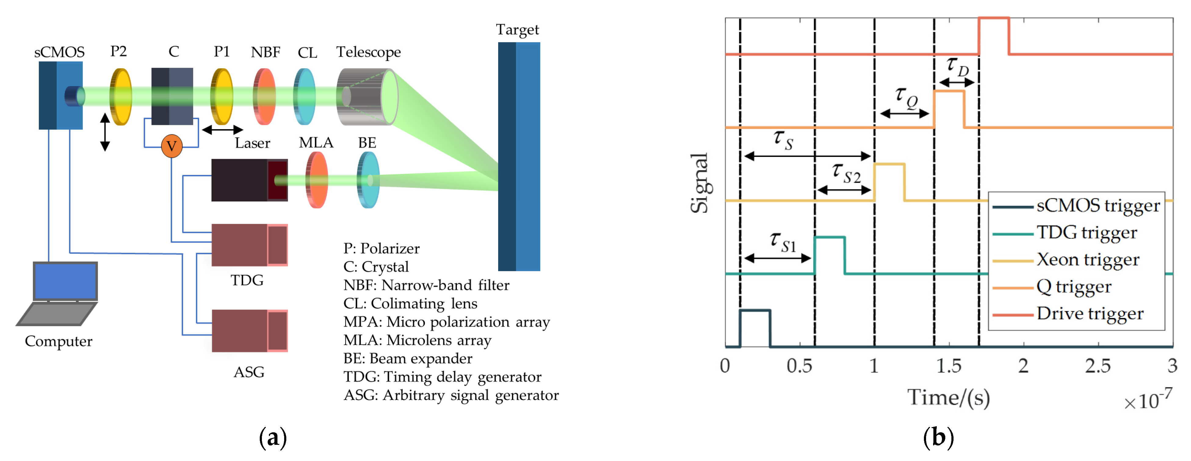
Figure 1. The system consists of a SCMOS camera, two polarizers, an electro-optical crystal, a narrow-band filter, a collimator, a receiving optical system, a pulsed laser, a microlens array, a beam expander, a delay signal generator, and a computer. Among them, the polarizer (P1 in
Figure 1), the analyzer (P2 in
Figure 1), whose polarization direction is perpendicular to the polarizer, and the electro-optical crystal constitute a crystal optical switch. The optical path can be switched on and off by changing the applied voltage of the crystal. The laser is a low-repetition-rate, high-pulse-energy, and narrow-pulse-width pulsed solid-state laser with a wavelength of 532 nm.
When the LIDAR system is working, a homogeneous and expanded pulse laser beam, whose pulse width is , is emitted at the target. When the pulse laser travels between the target and the receiving system, the applied voltage of the LN crystal is zero. Currently, the optical switch is in a closed state to prevent atmospheric backscattering and non-target scattering light. After the delay time , when the reflected light of the target returns to the receiving system, the stray light of other bands is filtered out first by the NBF (narrow-band filter), and then, under the control of the delay signal generator, a pulse voltage with a pulse width of and a pulse peak of the half-wave voltage of the LN crystal is added at both ends of the crystal.
At this time, the crystal electro-optical switch is on, and the SCMOS camera receives the reflected light of the target. After this process, the system completes the imaging of the target. The corresponding slice depth of field is:
where
c is the speed of light, and we can see from the formula that the crystal optical switch is only turned on for a short time so that the picture obtained by the SCMOS camera corresponds to a certain distance information. A series of distance-slice images can be obtained by changing the delay time
. The distance information of each image pixel can be calculated through the temporal and energy relationships between different slices. Then a three-dimensional image of the target can be obtained [
3].
The mainstream ranging algorithm is the weighted average method [
10]. This method is to multiply each gray value of the slice image sequence of the same pixel by a delay time serial number weight and divide it by the sum of all serial numbers to obtain an average image serial number. In order to calculate the distance, the average serial number is multiplied by the delay step and the delay time corresponding to the first image; this value is used as the flight time that corresponds to the target distance. This method has the advantages of high precision and fast operational speed.
According to the ranging principle above, the distance corresponding to the
ith image in the slice sequence image is:
where
represents the delay time corresponding to the
ith image,
represents the initial delay time, and
is the delay step. The average image serial numbers can be obtained as follows:
where
represents the gray value of each pixel in the
ith image. The range corresponding to each pixel can be obtained through the following formula:
When the range of the target point is determined according to the geometric relationship between the target image, the imaging optical system, and the target, the spatial position of the target point can be obtained, and the coordinates of each target point obtained can be converted into three-dimensional coordinates, and then the three-dimensional image of the target can be obtained by display processing.
3. Analysis of Electro-Optic Crystal Switch Inhomogeneity
We used a SCMOS camera to acquire the target image in our LIDAR system. As mentioned above, the SCMOS camera itself does not have a high-speed switch and thus can only obtain grayscale information. This means that it is necessary to use an optical switch that is composed of an electro-optical crystal and two polarizers to achieve slice imaging so that the gray value of the image can correspond to information at a certain distance.
The electro-optic crystal can be used as an optical switch mainly due to its conoscopic interference effect. The normalized light intensity of the central conoscopic interference pattern generated by the light passing through the optical switch is theoretically 0 when the voltage applied to the electro-optic crystal is 0. The electro-optic crystal optical switch can be regarded as being in an “off” state. Theoretically, the normalized light intensity of the central conoscopic interference pattern generated by the light passing through the optical switch is 1 when the voltage applied to the electro-optic crystal is half-wave. The electro-optic crystal optical switch can be regarded as being in an “on” state at this time. Compared with the switch of the ICCD cameras, the distribution of the conoscopic interference ring generated by the electro-optic crystal is not uniform, resulting in a deviation between the gray value of the image generated by the SCMOS cameras with electro-optic crystal switches and the SCMOS cameras with ideal switches. As can be seen from Equation (7) above, an electro-optic crystal switch will cause errors in the image sequence’s calculated mean, affecting the LIDAR system’s performance. An appropriate field of view needs to be selected to reduce this effect.
We chose an LN crystal as the electro-optic switch, and the inhomogeneity of the LN crystal was analyzed below. Combined with the light tracing analysis of the crystal with reference [
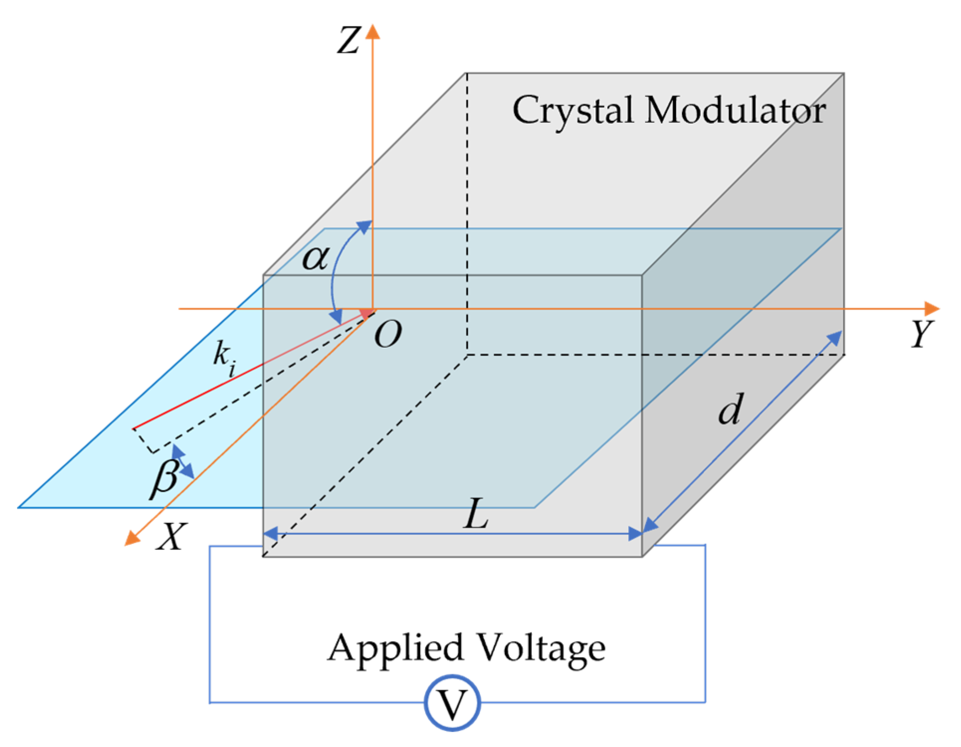
27], we can conclude that when the light travels along the crystal optical axis, the crystal phase difference delay caused by the electro-optic effect is:
The crystal conoscopic interference light intensity expression is:
where
is the zenith angle of the light incident to the electro-optical crystal,
is the azimuth angle of the incident light,
V is the applied voltage of the crystal,
is the refractive index of ordinary light in the crystal,
is the electro-optical coefficient of the crystal, and
L and
d are the length and thickness in the direction of the applied pulse voltage, respectively. It can be seen that the ordinary light refractive index
, electro-optical coefficient
, length
L, and thickness
d of the crystal are fixed values for a certain crystal, so the light intensity of the crystal is a function of
,
, and
V as variables. The influencing factors of the light intensity inhomogeneity of crystal switches are also mainly derived from
,
, and
V.
The influence of light intensity inhomogeneity is divided according to the abovementioned variables. The total inhomogeneity coefficient
is defined here, which represents the difference between the actual normalized light intensity received by a pixel on the detector and the normalized light intensity of the corresponding pixel in the center of the field of view on the detector, that is, the difference between the transmittance of the crystal optical switch of the pixel in the center of the field of view and the transmittance of the crystal optical switch corresponding to any other pixel. The inhomogeneity coefficient caused by the difference in incidence angles
and
(shown in the
Figure 2) is defined as
, representing the difference in transmittance of the crystal optical switch due to the influence of the conoscopic light interference effect. The inhomogeneity coefficient caused by the unideal pulse voltage
V is defined as
, representing the difference between the transmittance of the crystal under the actual non-ideal pulse voltage and the ideal pulse voltage. The total inhomogeneity coefficient is the sum of the two factors:
3.1. Analysis of Inhomogeneity Caused by the Angle of Incident Light of the Crystal
Firstly, the inhomogeneity caused by the different angles
of the crystal’s incident light is analyzed. According to Equation (6), the interference pattern of the crystal under ideal conditions is calculated and simulated using MATLAB, and the simulation result is shown in
Figure 3.
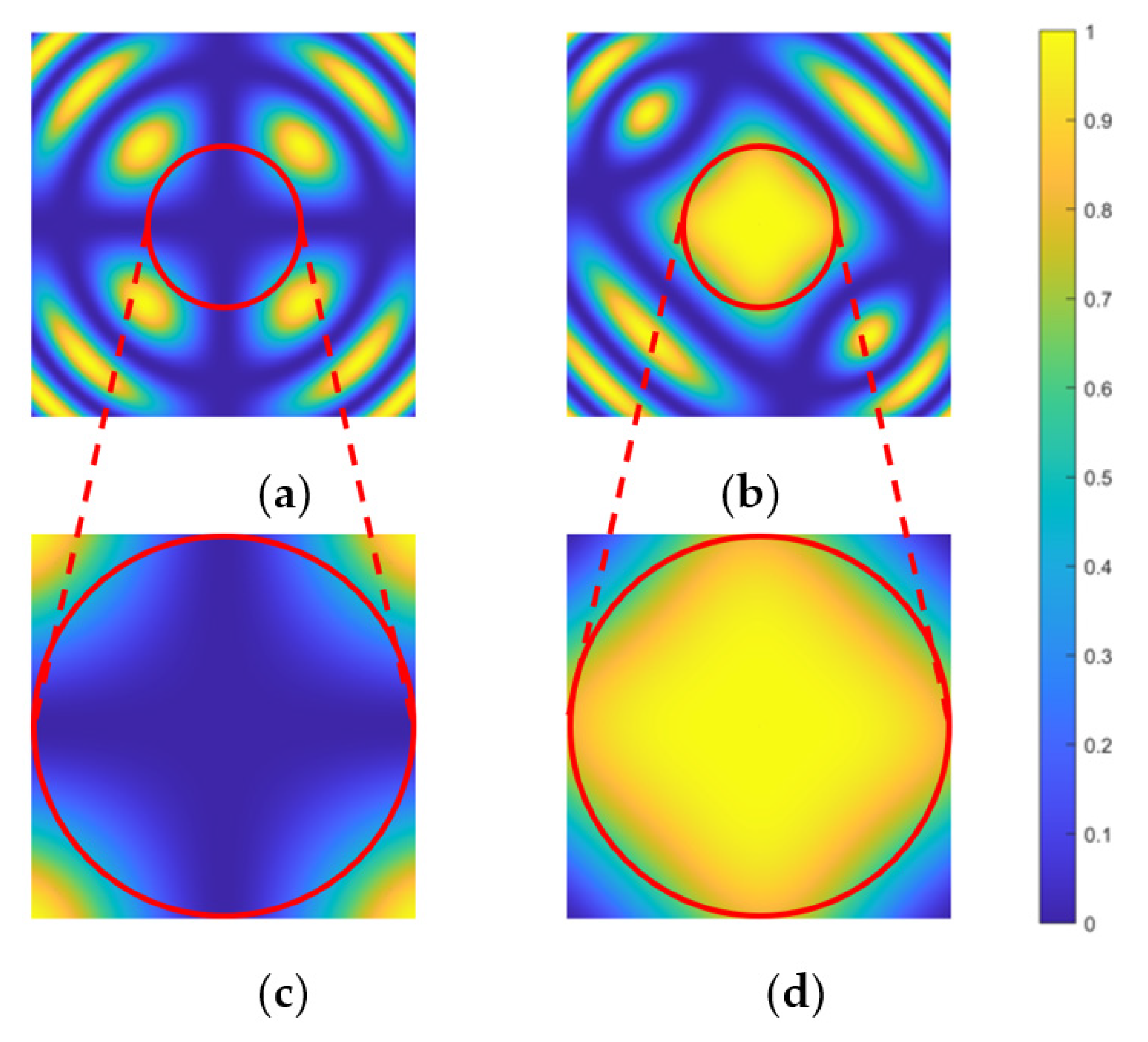
As shown in
Figure 3,
Figure 3a shows the normalized intensity distribution of light passing through the crystal when the voltage
V applied across the crystal is 0 and the field of view angle is 50 mrad.
Figure 3c is an enlarged view of the field angle range of 20 mrad in the center of
Figure 3a. From
Figure 3a,c, it can be seen that the uniformity of the image center is good, but the image uniformity is poor in the field of view edge areas at azimuth angles of 45°, 135°, 225°, and 315°. According to the MATLAB simulation results, at the center of the red circle, i.e., the central field of view, the normalized light intensity is 0. At the edge of the red box, which is the 20 mrad field of view angle, the normalized light intensity is 0.0168.
Figure 3b shows the normalized intensity distribution of light passing through the crystal when the voltage at both ends of the crystal is half-wave voltage
and the field of view is 50 mrad.
Figure 3d is an enlarged view of the field angle range of 20 mrad in the center of
Figure 3b. According to the simulation results, the normalized light intensity at the center of the field of view is 1, while at the edge of the 20 mrad field of view, the normalized light intensity is only 0.782.
From the simulation results, it can be seen that when LN crystals are used as optical switches, as the field of view angle changes, the normalized intensity of the transmitted light will change, thereby affecting the uniformity of the light intensity received by the detector.
According to the analysis above, based on the normalized light intensity value at the center of the field of view, when the applied voltage is a specific voltage
V, the difference between the normalized light intensity received by a pixel of the detector and the normalized light intensity received at the center of the field of view is:
3.2. Analysis of Inhomogeneity Caused by Unideal Pulse Voltage Applied to the Crystal
The inhomogeneity caused by the pulse voltage V applied to the crystal is analyzed below.
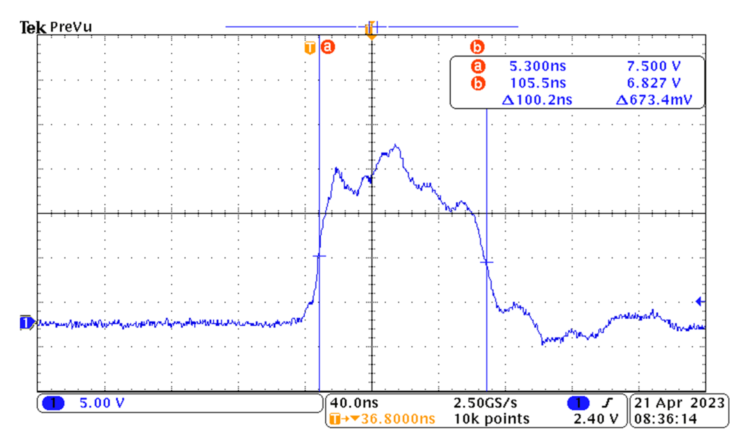
In order to calculate the inhomogeneity caused by pulse voltage, the pulse voltage applied to the electro-optical crystal should be measured with an oscilloscope. It can be seen from the measurement results below that the pulse width of the applied voltage source used in this research group is 100 ns.
Combined with Equation (6), the conoscopic interference pattern produced by the crystal is a function of voltage, and the corresponding conoscopic interference pattern is different for different voltages. The light intensity distribution detected on the detector during the process of applying a half-wave pulse voltage to the electro-optical crystal without considering the laser pulse waveform is:
Among them,
represents the light intensity of the image detected by the detector after one exposure,
represents the voltage value of the
ith sampling point on the oscilloscope,
n is the total number of the laser pulse voltage sampling points on the oscilloscope,
represents the light intensity corresponding to the crystal conoscopic interference pattern when the voltage applied to the crystal is
, and
represents the normalized light intensity of the laser pulse received by the crystal when the voltage is
. When the ideal electro-optic crystal switch is open, the voltage applied at both ends should be the half-wave voltage of the crystal. As shown by the waveform of the crystal external driving power supply displayed on the oscilloscope in
Figure 4, there is a significant error between the crystal external pulse voltage and the ideal pulse half-wave voltage. The non-uniformity coefficient corresponding to the light intensity error caused by the imperfect pulse voltage is calculated with Equation (10).
In this formula,
is the normalized conoscopic interference light intensity corresponding to the half-wave voltage.
Combining the influence of the conoscopic interference effect of the LN crystal and the non-ideal pulse voltage, the total inhomogeneity coefficient generated by the electro-optic crystal optical switch can be obtained by bringing Equations (8) and (10) into Equation (7):
When the voltage at both ends of the crystal is half-wave voltage
, the formula can be simplified as:
Based on the non-uniformity analysis discussed above, we used MATLAB R2021a software to simulate the imaging results of the system.
Figure 5 shows the temporal relationship between the laser pulse and the voltage applied to the crystal.
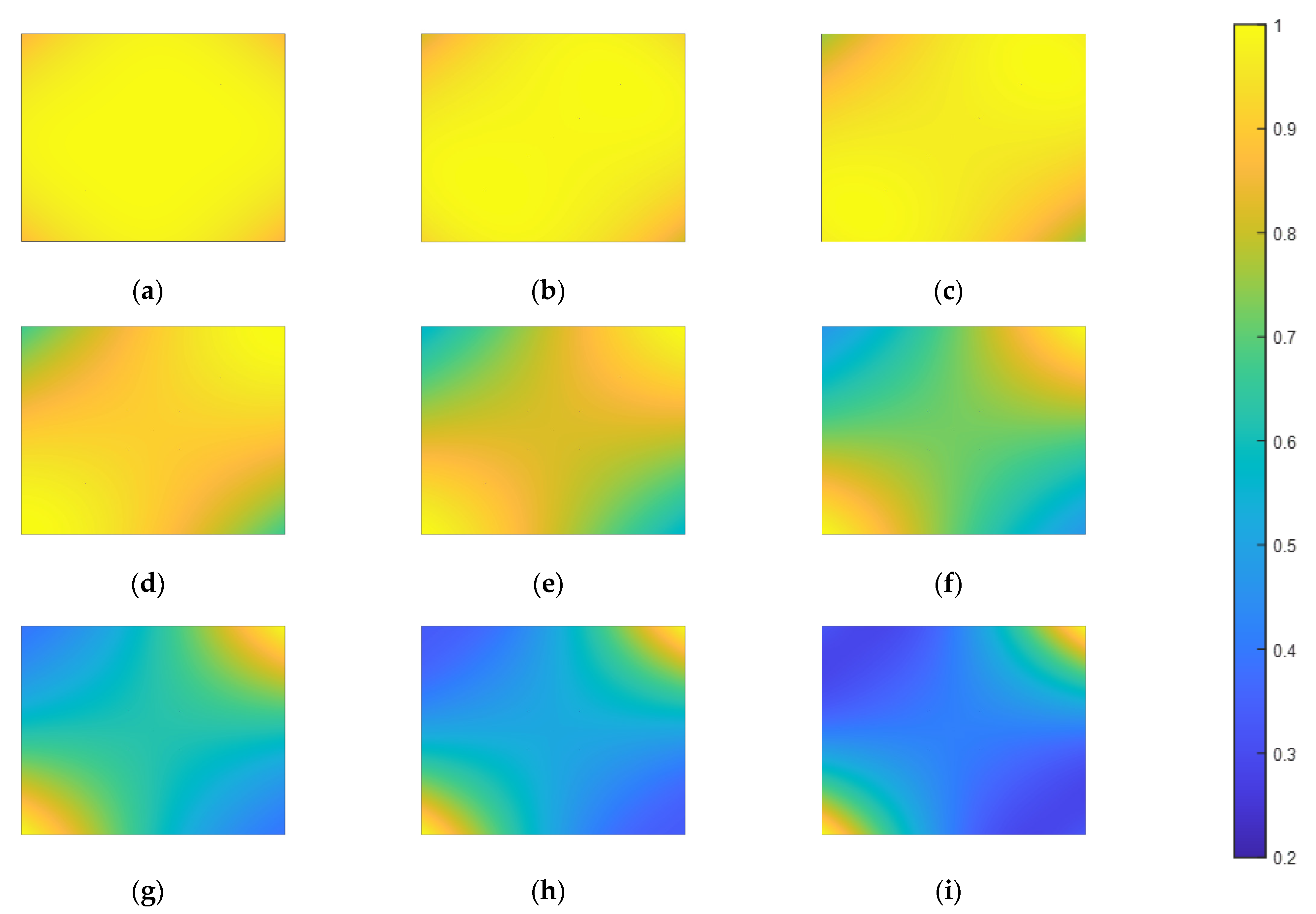
Figure 6 shows the results of gated imaging of planar targets by a range-gated LIDAR system using an LN crystal as a switch under ideal conditions. The relationship between the pulse voltage applied to the crystal and the laser pulse corresponding to the simulated imaging results in
Figure 6a is shown in
Figure 5a. Additionally,
Figure 6b–i shows the simulation images corresponding to the increase in the gating delay by 4 ns, respectively. The relationship between the pulse voltage applied to the crystal and the laser pulse corresponding to the simulated imaging results in
Figure 6i is shown in
Figure 5b. Combined with
Figure 5, when the laser pulse entirely coincides with the pulse voltage applied to the crystal in a time sequence within a 2.6 mrad field of view, the maximum normalized light intensity in the simulation image
Figure 6a is 1, and the minimum normalized light intensity is 0.96, which can be regarded as the case where the plane target is completely gated. With the increase in delay time, the coincidence region of the laser pulse and the pulse voltage applied to the crystal gradually decrease, and only part of the laser pulse is gated. The normalized light intensity of the image decreases from both ends to the center, and the normalized light intensity of the image’s upper-left and lower-right ends is significantly higher than that of the lower-left and upper-right ends. The simulation results reflect the apparent inhomogeneity of the system slice image.
3.3. A Compensation Method for Crystal Inhomogeneity
According to the above analysis of the source of electro-optical crystal switch inhomogeneity, the compensation method for crystal inhomogeneity is studied. In the actual compensation process, not only the relationship between the crystal ideal matrix, the inhomogeneity matrix, and the compensation matrix should be considered, but also a certain extinction ratio of the switch should be taken into consideration as the actual switch is not ideal.
We define the transmittance matrix represented by
as the full
matrix, and
represents the transmittance of the ideal switch under a certain voltage applied to the crystal. The actual electro-optic crystal switch transmittance matrix is defined as
, and the transmittance of the center field of view in
should also be
. The inhomogeneity matrix calculated by Formula (12) is defined as
, the actual inhomogeneity matrix considering the extinction ratio is defined as
, the compensation matrix is
C, and the extinction ratio matrix is defined as
. Then
can be calculated using the following equation:
In the formula above,
represents a matrix with all values of 1, and
is the maximum value function that is used to normalize the matrix. After obtaining the actual inhomogeneity matrix, the compensation matrix
can be calculated using the following formula:
For the slice image captured by the experimental LIDAR system, the image compensating the inhomogeneity of the electro-optic crystal switch can be obtained by multiplying pixel by pixel with the corresponding compensation matrix. It should be noted here that according to Equation (1), the slice image obtained has a certain depth of field, meaning that a slice image may contain laser pulses reflected by targets at different distances. The time of flight of the laser pulse reflected from different distances is different, and the applied pulse voltage of the crystal corresponding to the laser pulse received by the system at different times is also different, resulting in different transmittances of the electro-optic crystal switch. When the pulse width of the pulse voltage applied to the crystal and the laser pulse width of the crystal are large, the interference state of the electro-optic crystal switch corresponding to the target at different distances on a single slice image is quite different. At this time, when the compensation matrix corresponding to a specific time is applied to the slice image, a more significant error might be introduced. The compensation matrix can only be used when the laser pulse width and the pulse width of the voltage applied to the crystal are small to a certain extent.
4. Experiment and Analysis
Table 1 shows the main parameters of the experimental LIDAR system. The experimental system of the proposed range-gated experimental LIDAR using an LN crystal as an optical switch is shown in
Figure 7.
Figure 8a is the optical layout of the experimental system. As shown in
Figure 7 and
Figure 8a, we use a Tektronix’s AFG 31,000 SERIES arbitrary signal generator (ASG) and a Fastlaser.Tech’s TDG-VII timing delay generator (TDG) to realize the synchronous control of the crystal voltage driver, SCMOS camera exposure control, laser pulse xenon lamp signal, and Q-switched signal. Since the ASG we use produces up to two signals, the TDG produces a delay of up to 1 ms, which is less than the exposure delay of the PCO Edge.55 SCMOS camera, and the TDG’s jitter time in the external trigger mode is much smaller than the corresponding jitter time when using the internal clock, we chose to combine the signal generator and the signal delayer to achieve synchronization control of the entire experimental system.
As shown in
Figure 8a, when the system is working, the ASG generates a signal without delay and a signal with a delay of
to trigger the SCMOS camera and the TDG, respectively. After the TDG is triggered, the trigger signal generated by the TDG triggers the laser xenon lamp, the Q-switched switch, and the driver of the LN crystal. The delay
between the xenon lamp trigger signal and the Q-switched trigger signal is the Q-switched delay of the laser, and the delay
between the Q-switched trigger signal and the driver of the LN crystal trigger signal is the range-gated delay. As shown in
Figure 8b, when the laser is triggered, a pulsed xenon lamp-pumped Nd:YAG Q-switched laser emits a pulsed laser with a pulse width of 7 ns and a spot distribution similar to a Gaussian distribution at the target. The pulsed laser first reaches the microlens array and is homogenized, then reaches the beam expander and is expanded by it. After that, the pulsed laser propagates to the target and is reflected by the target. The reflected laser pulse first reaches the telescope with an aperture of 90 mm and an F number of 1:5.5, and after being received by the telescope, it reaches the collimator CL and is collimated. The collimated laser pulse then reaches the NBF and filters out the stray light of other wavelengths, thereby improving the signal-to-noise ratio of the system. After passing through the NBF, the laser pulse reaches an optical switch composed of polarizer P1 with a horizontal polarization direction, an LN crystal C with a length and width of 9 mm and a thickness of 18 mm, and polarizer P2 with a vertical polarization direction. If the crystal optical switch is closed under the action of the driving voltage at this time, the pulsed laser is blocked by the optical switch, and the SCMOS cannot receive the laser pulse. If the crystal optical switch is turned on under the action of the pulse voltage at this time, the laser pulse is received by the SCMOS camera, thus enabling a range-gated image of the target.
In order to verify the accuracy of the compensation method, a pure white plate is placed 22.04 m away from the receiving system, and a gated imaging experiment on the white plate is conducted. The effect of imaging compensation is shown in
Figure 9. From
Figure 9a, we can see that because the physical principle of the crystal as an optical switch is the conoscopic interference effect of the crystal, only the area of about 301
301 pixels in the center of the field of view can achieve uniform imaging.
Figure 9c,d are the contrast images of the imaging effect of the 601
601 pixel range area of the crystal center before and after compensation. From the image effect before and after compensation, it can be seen that in the pixel area taken, the gray image uniformity of the target imaging is significantly improved, proving the algorithm’s accuracy.
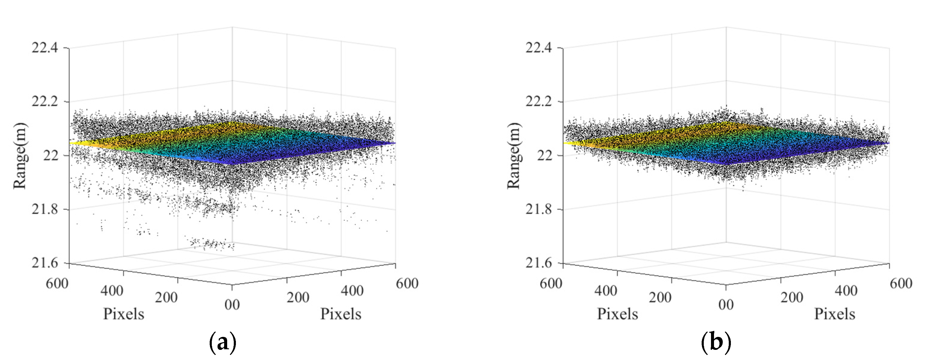
Using the slice image before compensation and the slice image after compensation for three-dimensional reconstruction, the obtained point cloud images areshown in
Figure 10.
Figure 11 are the distance depth maps of the flat target obtained by the system before and after compensation.
Figure 12 shows the comparison of the distance depth with the horizontal row of pixels, where the orange curve represents the distance depth curve in
Figure 11b, the green curve represents the distance depth curve in
Figure 11a, and the blue line represents the true distance of the target.
Figure 12a–c represent the average distance depth of the first to fifth rows of pixels in
Figure 11, the average distance depth of the 299th to 303rd row of pixels, and the average distance depth of the 597th to 601st rows of pixels, and these pixels are marked with solid black translucent lines, respectively, in
Figure 12a,b. From
Figure 10,
Figure 11 and
Figure 12, we can conclude that due to the influence of the inhomogeneity of the electro-optical crystal switch, the calculated value of the distance depth is generally smaller than the true value in the upper-left and lower-right parts of the distance depth image calculated by the original slice image, while the calculated value of the distance depth is generally larger than the true value in the lower-left and upper-right parts of the image. Additionally, there are obvious isolated points at the edge of the point cloud image. The range accuracy of the depth image restored by the compensated slice image is significantly improved in the corner part; the tilt phenomenon is obviously suppressed; the isolated points of the image in the edge part are significantly reduced; and the image dispersion in the center part is reduced. This result verifies the accuracy of the compensation method.
The distance accuracy of the image within a 2.6 mrad field of view is calculated as follows:
In the formula,
represents the standard deviation of distance depth,
n represents the total number of pixels,
represents the distance corresponding to the ith pixel, and
represents the actual measured target distance with a fixed value of 22.04 m. After calculation, the standard deviations of the distance depth corresponding to
Figure 11a,b are 3.86 cm and 2.86 cm, respectively. Additionally, the standard deviations of the distance depth of the areas marked with red boxes in the upper-left, upper-right, lower-left, lower-right, and central field of view in
Figure 11a are 4.26 cm, 3.18 cm, 2.71 cm, 5.05 cm, and 2.69 cm, respectively, and in
Figure 11b, the standard deviations are 2.53 cm, 2.38 cm, 2.56 cm, 2.81 cm, and 2.30 cm, respectively. Among them, the standard deviation of the distance depth of the marked area in the upper-left and lower-right parts decreased significantly, indicating that the tilt phenomenon caused by the crystal switch was significantly suppressed, which verified the accuracy of the compensation method. The leading causes of range error are as follows: First, the pulse voltage applied to the crystal is not an ideal pulse, and its peak waveform stability is poor. In this case, there will be errors when the sequence image weighted average method is used to recover the distance depth. Second, the principle of the crystal as an optical switch is the conoscopic interference effect of the crystal. The conoscopic light interference effect itself has inhomogeneity, and there will be a significant error at the edge of the field of view. Third, the jitter time of the TDG triggering the crystal pulse voltage is 25 ps according to the product manual, and the corresponding ranging error is 0.38 cm. The shot noise of SCMOS will also cause a particular distance error. After compensation, the influence of the first and second reasons is obviously suppressed, and the standard deviation of system distance depth is obviously improved.
5. Conclusions
In this paper, a range-gated LIDAR system using an electro-optic crystal as the optical switch is designed. The slice image of the target is obtained by synchronously controlling the pulse voltage applied to the crystal, laser pulse, and SCMOS exposure, and then the three-dimensional point cloud image and distance depth image of the target are reconstructed using the slice image.
Compared with the traditional range-gated LIDAR system using an ICCD as an imaging device, a high-precision sequential logic circuit and high-bandwidth detector must be used to improve the range accuracy. For the system designed in this paper, the use of the SCMOS detector only needs to detect the intensity of the reflected laser of the target instead of detecting the time of flight (TOF) and does not require a high-precision sequential logic circuit, which greatly reduces the cost of the system.
However, compared with the built-in shutter ICCD, the use of an electro-optic crystal as a light shutter will introduce new inhomogeneity errors, which will affect the ranging accuracy of the system. To reduce the impact of this error, this paper quantitatively analyzes the source of the crystal inhomogeneity error, proposes a compensation method for crystal inhomogeneity, and gives the mathematical expression of the inhomogeneity compensation matrix. The experimental results show that compared with the range depth image restored by the original slice image, the accuracy of the compensated range depth image is significantly improved, and the standard deviation of the range depth is reduced from 3.86 cm to 2.86 cm within a 2.6 mrad field of view, which verifies the accuracy of the algorithm and provides a guarantee for further improving the performance of the system.

