Review

Toward Practical Optical Phased Arrays through Grating Antenna Engineering

1
Key Laboratory of Optoelectronic Materials Chemistry and Physics, Fujian Institute of Research on the Structure of Matter, Chinese Academy of Sciences, Fuzhou 350002, China
2
University of Chinese Academy of Sciences, Beijing 100049, China
3
State Key Laboratory of Advanced Optical Communication Systems and Networks, School of Electronics, Peking University, Beijing 100871, China
4
Beijing Aijie Optoelectronic Technology Co., Ltd., Beijing 100190, China
5
Fujian Science & Technology Innovation Laboratory for Optoelectronic Information of China, Fuzhou 350108, China
*
Authors to whom correspondence should be addressed.
Photonics 2023, 10(5), 520; https://doi.org/10.3390/photonics10050520
Submission received: 31 March 2023 / Revised: 25 April 2023 / Accepted: 27 April 2023 / Published: 1 May 2023
(This article belongs to the Special Issue Advances in Optical 3D Integration)

Abstract

:
In recent years, using silicon-based waveguide grating antennas in optical phased array has become a research focus. To date, this technique has not been widely implemented in practical applications. In this paper, the basic principle of a waveguide grating antenna is described, and the researches on effective length, uniform emission and the directionality of diffraction are summarized. Through analysis, it is found that there is a trend to prepare grating antennas by using a SiN/Si hybrid integrated platform. A novel design of grating antenna using the hybrid integration technique is proposed. It is convenient to match with the antenna front-end components on the structural level and is more practical.

1. Introduction

Waveguide grating devices have been widely used in silicon-based optoelectronics because of their excellent performance. Grating devices, possessing periodic optical properties, can be widely used as functional elements. In the field of silicon-based optoelectronics, grating is often used to achieve light coupling [1], beam shaping [2], mode selection [3,4] and other functions.
Phased array antenna was first proposed in the early nineteenth century and its complete theoretical framework had been established since then. As an important component in radar systems, the phased array antenna controls beam emission and steering through phase modulation. Microwaves and optical waves are both electromagnetic waves and therefore have similar propagation properties. However, compared with microwave, the wavelength of light wave is much shorter, so it is difficult to control the phase. It was not until the 1970s that great progress was made in the research of optical phased array [5,6]. With the technological development of various related fields, optical phased array has gradually become a research hotspot in free space optical communication and Lidar system. Due to the development of autonomous driving and other fields, the need for on-chip lidar is urgent. The development of silicon-based optoelectronic technology has greatly promoted the development of on-chip integrated lidar. The high integration degree, compatibility with CMOS technology, and photoelectric monolithic integration of silicon-based optoelectronic technology provide a very broad prospect for the realization of on-chip lidar chip [7,8,9,10,11,12].
As one of the key elements of silicon-based optical phased arrays, the grating antenna can carry out a large range of two-dimensional arrangements on a chip, and the beam will be emitted to the free space due to diffraction. As an emission unit, there are many research works on grating antennas, and the contents of the studies are varied. However, most of the current studies are aimed at improving a specific property, and they rarely consider the design alignment accuracy and complexity of the fabrication process. To enable large-scale application, grating antennas must have an excellent performance with a simple fabrication process. Therefore, when designing grating antennas, practicality should be given greater consideration.
In this paper, the basic principle of a waveguide grating antenna is described in Section 2. In Section 3, the related research works are divided into the effective length, uniform radiation, and the directivity of diffraction, and a research idea based on hybrid integrated platform is proposed. In Section 4, the current research trends of grating antennas and how to develop them toward the practical applications are discussed. Finally, a summary is made in Section 5.

2. Basic Structure and Principle

Waveguide grating antennas can be classified into one-dimensional and two-dimensional [13]. The latter requires more phase shifter arrays and electrode connections than the former, which will be much more complicated when the arrays grow larger and bring great limitations and challenges to the layout of on-chip integration. The main content in this paper will therefore focus on the one-dimensional arranged waveguide grating device as shown in Figure 1a.

2.1. Basic Structure of Waveguide Grating Antenna

In the field of silicon-based optoelectronics, grating devices are mainly used in grating couplers [14], grating mirrors [15] and direction couplers and so on. As a kind of grating device, the structure of a grating antenna has periodic dielectric perturbation in the propagation direction of the optical mode. These perturbations can be achieved by adjusting the physical structure of the device or changing the refractive index through the alternation of different materials. As light propagates to each boundary, it is reflected or diffracted. Periodic repetition of the interface will result in multiple reflections and diffraction, so that the reflected or diffracted light will interfere with each other in one direction. Figure 1a shows a common waveguide grating antenna element structure. The light is transmitted to free space by diffraction when it passes through a grating array, and then the light emitted by each waveguide interferes with each other in space, as shown in Figure 1b, and finally forms a diffractive beam.

2.2. Basic Diffraction Principle of Waveguide Grating Antenna

Figure 2a shows the simplest diffraction grating. The incident wave is the plane wave, β is the incidence angle of the incident beam to the grating, and α is the diffraction angle. Two diffraction beams from two adjacent slits with emission angle α have different phases, and the optical path difference corresponding to the phase difference between them is d (sinα + sinβ). When the optical path difference is an integral multiple of the wavelength, constructive interference occurs:
d   ( sin α + sin β ) = m λ   ;   m = 0 ,   ± 1 ,   ± 2 ,  
where d is the distance between the two slits, λ is the wavelength of incident light, and m is the order of diffraction order. It should be noted that this formula corresponds to transmission grating, and sinβ is negative for reflection grating.
In particular, this is the case in Figure 2b when the incident light is perpendicular to the slit. The optical path difference corresponding to the phase difference of two diffracted beams from two adjacent slits is dsinα. Therefore, when the optical path difference is an integral multiple of the wavelength, the grating equation is:
d sin α = m λ ;   m = 0 ,   ± 1 ,   ± 2 ,  
Similarly, for the simplest grating antenna structure as shown in the Figure 2c, the phase difference of two diffracted beams with a diffraction angle of θ from two adjacent diffraction points corresponds to an optical path difference that is an integer multiple of the wavelength:
n eff d n 1 d sin θ = m λ ;   m = 0 ,   ± 1 ,   ± 2 ,  
where n1 is refractive index of the corresponding region in the figure, and neff is the effective index of the grating region.
The m-order diffracted wave vector Km can be calculated from Equation (4):
K m = 2 π λ n  
where λ is the free space wavelength and n is the refractive index of the corresponding material.
According to Equations (3) and (4), it can be obtained that:
K m = β     m K  
where β = neff (2π/λ) is the waveguide propagation constant, K = 2π/d is the grating vector.
Equation (5) is the basic relation of grating antenna—the Bragg condition. The Bragg condition describes the relation between the incident wave vector and each diffraction wave vector, which is the most basic relation in grating devices.
It needs to be emphasized that the derivation process is based on the Fresnel–Kirchhoff diffraction integral, and the theory itself has some inconsistence, so the Bragg condition can only be used as a reference for the design. In practice, we need to use the finite-difference time-domain (FDTD) or rigorous coupled-wave analysis (RCWA) algorithm for accurate calculation.

3. The Main Research Directions of Waveguide Grating Antenna

Thanks to the rapid development of silicon-based optoelectronic technology and the urgent demand of autonomous driving, on-chip integrated solid-state lidar is in the hot spot of research. As one of the important modules, the waveguide grating antenna is the focus of research [16]. The research on grating antenna structure can be divided into three directions. The first is how to improve the effective length of the grating antenna, the second is how to achieve uniform radiation, and the third is how to achieve high directivity during transmission. The following is an analysis from these three aspects.

3.1. The Effective Length of a Waveguide Grating Antenna

When light is transmitted in a waveguide grating antenna with uniform grating, the remaining energy in the waveguide decays exponentially:
I x = I 0 exp α x  
where I(x) represents the remaining light energy when the light is transmitted to x position, taking the beginning of the grating as the origin position, I0 represents the energy input to the grating, and α is the attenuation coefficient.
When I(x) ≈ 0, the light has been completely emitted here, and then the length is the effective length of the grating antenna. For grating antennas, the effective length is an important parameter, which determines the divergence angle of the spot. For a grating antenna with uniform diffraction intensity, the divergence angle can be calculated by the formula:
Δ θ = 0 . 886 λ N Λ cos θ rad  
where refers to the effective length of the grating. λ refers to the wavelength of incident light; and θ refers to the far-field diffraction angle.
In the application of Lidar and other fields, we need more concentrated energy of far-field light spots in order to obtain higher detection accuracy, larger detection range, and higher resolution. The larger the effective length of the grating antenna, the smaller the divergence Angle of the far-field spot can be obtained [17]. Thus, the divergence of the beam is determined by the effective length of the grating antenna, and the length of the grating is determined by the degree of light limitation in the transmission waveguide. Therefore, in a Si/SiO2 platform with high restriction, even a small refractive index disturbance will produce strong grating diffraction intensity due to a high refractive index contrast. Therefore, the length of grating antennas made on Si/SiO2 platforms is usually small and the beam divergence is serious. In contrast, on the SiN/SiO2 platform, the refractive index contrast is relatively low, leading to a smaller refractive index disturbance generated by the same etching process. As a result, the grating strength is weaker, and it becomes easier to achieve a millimeter effective length. Nevertheless, the Si/SiO2 platforms have their own advantages, such as a compact layout due to high refractive index contrast.
As shown in the Figure 3a, the traditional grating antenna is etching on the Si waveguide. Since the refractive index of SiN is small relative to the refractive index of the Si, the disturbance caused by the placement of the SiN strips on the Si straight waveguide is smaller than that caused by the placement of the Si strips. Therefore, the disturbance of the optical mode is also smaller when the light propagates, so the diffraction intensity is weak, which increases the effective length. Moshe Zadka et al. implemented a millimeter grating antenna based on the Si waveguide by placing the SiN strips on the Si straight waveguide and obtained a divergence angle of only 0.089° [18].
As shown in the Figure 3b, increasing the gap between the grating teeth and the transmission waveguide can reduce the refractive index perturbation intensity and thus increase the effective length. Qing Wang et al. used this similar structure to make SiN-assisted grating antennas of different lengths [19]. A 2 mm emission length is achieved by adjusting the period and duty ratio, and the beam divergence angle is only 0.075°. In the study of the relationship between the beam evolution in phased array optics and the aperture size, Weihan Xu et al. fabricated a grating antenna of similar structure with a length of 10.3 mm, where the SiN grating teeth were separated from the Si waveguide [20].
Jiaxin Chen et al. theoretically proposed and demonstrated a millimeter-level waveguide grating antenna with a divergence angle of 0.081° [21]. This structure is achieved by placing the subwavelength Si segments with easily fabricated subwavelength structures on both sides of the Si waveguide. The grating coupling strength can be adjusted to achieving an effective length of several centimeters by adjusting the size and position of the Si segment. Pablo Ginel-Moreno et al. used a metamaterial subwavelength grating waveguide core loaded with a transverse periodic array of radiating elements to fabricate a 2-mm-long ultra-long antenna in silicon waveguides [22,23]. Weak antenna radiation strength was achieved while maintaining a minimum feature size of 80 nm, and a far-field divergence angle of 0.1° was measured.
Table 1 summarizes the structures and features mentions in this section. In conclusion, many grating antennas can reach the magnitude of millimeters in these special structures.

3.2. Uniform Radiation

As described in Section 2.1, for an antenna with uniform grating diffraction intensity, the remaining energy in the waveguide decays exponentially, so most of the energy is emitted as soon as it enters the grating antenna, which makes the effective length of the antenna smaller than the actual length. Therefore, it is also a hot research topic to design a reasonable structure to achieve uniform emission.
According to Formula (6), the following formula can be obtained:
I ( x ) = I 0 exp 0 x α t dt  
In order to obtain a uniform emission pattern, the following formula needs to be satisfied:
W ( x ) = d dx I ( x )   = C  
W(x) is the radiated power at position x, and C is a constant.
By utilizing numerical simulation, linear fitting, and other methods to establish the relationship between the perturbation and radiation coefficient, one can derive the differential equation above to satisfy the required values of each parameter. The uniform emission of the grating antenna also increases the effective length of the grating antenna as much as possible. Through the special design of apodization, most of the energy will not be emitted immediately after entering the grating antenna, so that the diffraction intensity of the beam at each diffraction point of the grating antenna is uniform.
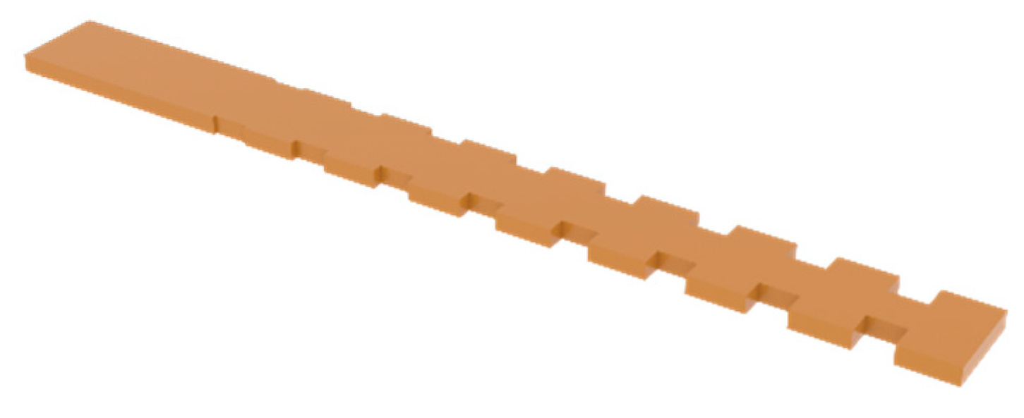
For traditional straight waveguide grating, uniform emission can be achieved by adjusting the width of the etching holes to change the radiation coefficient. For fishbone grating, uniform emission can also be achieved by chirp design. The chirp design can adjust the diffraction intensity at each diffraction point. Figure 4 shows the chirp design of a fishbone grating antenna. Lei Yu et al. compared two kinds of grating antennas with chirped grating and uniform grating by the fishbone grating antenna [24]. Based on the theoretical and experimental results, the chirp design realized uniform radiation. Hongjie Wang et al. realized a uniform emission mode with a wavelength ranging from 1450 nm to 1650 nm by adjusting the pitch of the fishbone grating and the depth of the grating teeth [25].
As shown in Figure 5, the grating strength of each point can be adjusted by adjusting the duty ratio and width of the top layer SiN with the SiN/Si double-layer structure. Uniform transmission can be achieved through design, thus increasing the effective length of the grating antenna to the order of millimeter [26,27]. Compared with controlling the width of etching holes on the waveguide, it is easier to realize the ultra-long grating antenna in this multilayer structure due to the smaller refractive index disturbance of SiN.

3.3. The Directivity of Diffraction

The input optical power in chip integration is generally small, so it is required to reduce the energy loss as much as possible. As an optical antenna, higher output optical power means higher signal-to-noise ratio and larger detection range. Due to the vertical symmetry of diffraction, the traditional grating structure will radiate almost equal optical power to the upper and lower directions. Therefore, factoring in the diffraction directivity becomes imperative during the design process of a grating antenna. By designing a specific structure to break the vertical symmetry of diffraction, the high directivity of diffraction can be realized. In the research on grating couplers, how to reduce the diffraction loss in the direction of the substrate in the coupling process is also a problem of the diffraction direction. For example, methods to increase the coupling efficiency of the grating couplers such as deep etching [28] and binary blazed grating [1,15] have been reported. However, the length of the grating coupler is generally small, so the reported structure is generally difficult to be directly applied to the grating antenna.
As shown in Figure 6a, a multilayer misaligned waveguide grating structure can realize the unidirectional emission. The multilayer misaligned structures can be separated scattering elements or misaligned etched on the upper and lower surfaces of a single waveguide [17,29,30]. Manan Raval et al. demonstrated a waveguide grating antenna with unidirectional emission of millimeter-sized [17]. The misalignment of the two fishbone grating layers in the direction of propagation achieved over 90% directionality, because upward constructive interference and downward destructive interference. Pengfei Ma et al. placed the same misaligned grating structure scatterers above and below the transmission waveguide, respectively, and achieved an upward directionality is 96.7% at 957 nm [29]. Baisong Chen et al. designed similar dual-chain and dual-fishbone structure grating antennas, both of which achieved over 90% unidirectional emission [30].
As shown in the Figure 6b, a waveguide grating is placed on the base transmission waveguide to form a double-layer structure to achieve high directionality. Light propagates in the bottom waveguide and enters the upper waveguide grating by evanescent coupling. Finally, diffraction occurs in the waveguide grating, and the light is emitted into free space. Qing Wang et al. proposed a SiN/Si dual-layer grating antenna based on this structure. The lower layer is the Si transmission waveguide, and the upper layer is the SiN waveguide grating. This structure achieves more than 89% directionality [31]. Chenyang Mei et al. also adopted this structure with SiN in the upper and lower layers and achieved directionality of over 50% [32].
P.F. Wang et al. proposed a new type of optical antenna, which uses the high-contrast grating structure in the grating antenna to achieve extremely efficient emission [33], with the emission efficiency up to 93.94% at the wavelength of 1.55μm. The cross-section structure is similar to Figure 3b.
Yu Zhang et al. added Distributed Bragg Reflectors (DBR) at the bottom of the grating antenna and optimized the thickness and spacing of each layer through simulation [34]. The results showed that the unidirectional transmission efficiency of the grating antenna increased from 46% to 95% after the DBR were added. Shahrzad Khajavi et al. achieved an emission efficiency of 82% while designing a nanophotonic antenna based on near-field phase engineering, by incorporating a bottom Bragg reflector into the structure [35], but this structure in the process of production is more complicated.
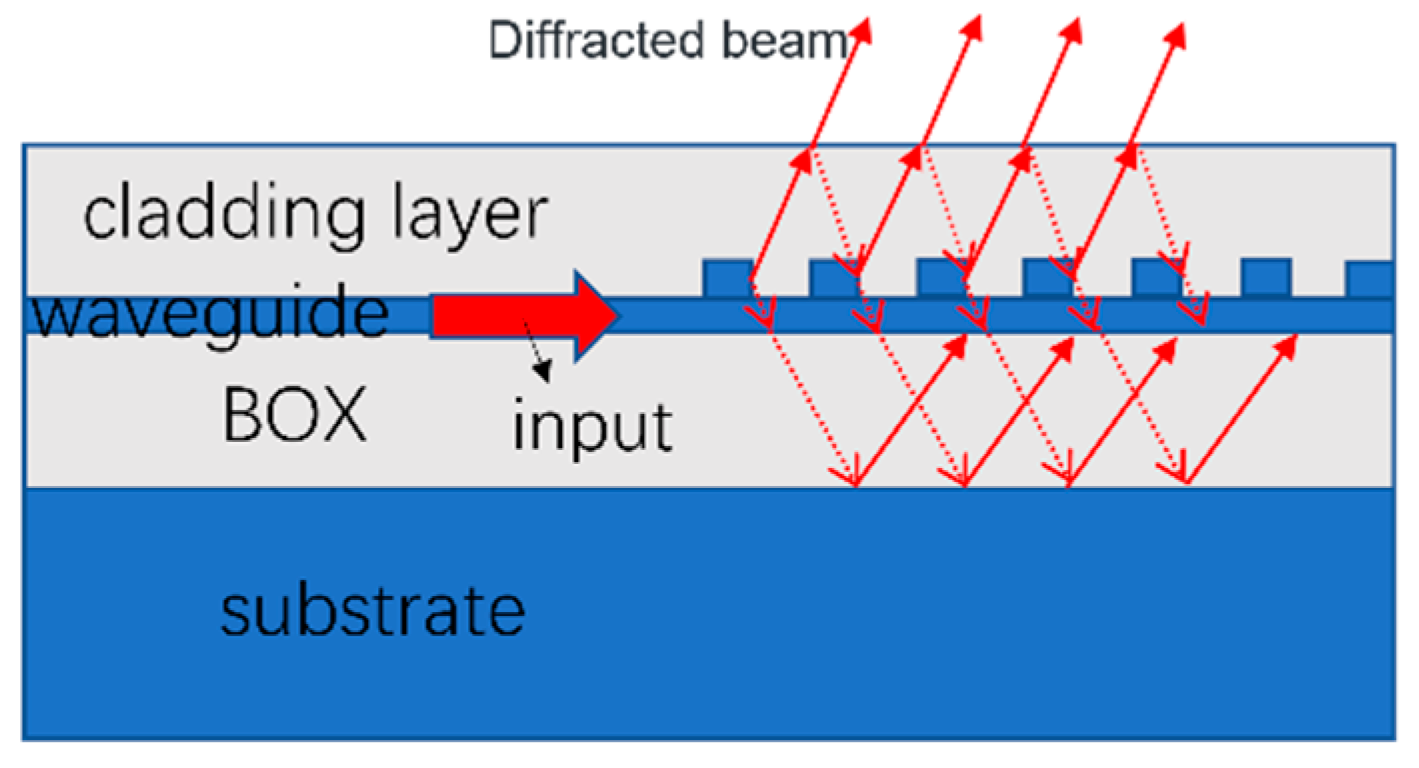
As shown in the Figure 7, from the perspective of longitudinal interface, the traditional silicon-based grating antenna structure is generally composed of buried oxide, waveguide grating, and upper cladding, so this structure can be described as having a cavity configuration. Ghul-Soon Im et al. researched the effect of the optical thickness of the cavity on the diffraction direction, and confirmed through theory and experiment that the optimal emission efficiency would be generated when the optical thickness was equal to the odd integer multiple wavelength of a quarter wavelength [36]. Guangzhu Zhou et al. proposed a compact aperture coupled nanoslot antenna array [37]. This structure consists of a high-contrast grating structure and a silver patch with H-type nanoslot on the top layer. This structure combines the low loss characteristic of hybrid plasma waveguide with the high reflectivity characteristic of high-contrast grating and achieves the maximum emission efficiency of 87.6% in the bandwidth of 1500 nm~1600 nm. However, this kind of structure is difficult to adapt to traditional CMOS technology.
Here we propose a novel design of a grating antenna to achieve highly directional radiation. SiN and Si gratings are placed on the upper and lower of the SiN transmission waveguide to break the vertical symmetry and achieve highly directional radiation. This design method that utilizes two different scattering structures to improve coupling efficiency has been reported in grating couplers [38], but has not yet been applied in grating antennas. Different from the three-layer structure mentioned in [10], this structure can achieve high emission efficiency. Moreover, the parameters such as the height and pitch of the SiN waveguide and Si grating can be matched with front-end components for overall design.
Table 2 summarizes the structures and features mentions in this section. For chips, the energy loss of more than 50% of the conventional grating structure is difficult to accept, so there is more research on the directivity of antenna. At present, except for some special structures, most of the diffraction structures are set up to break the upper and lower symmetry of diffraction, so as to achieve the purpose of unidirectional diffraction. In this research, multi-layer structure has also found numerous applications.

4. Discussion

There are many research works on silicon grating antennas, but none of them can be widely used by the industry at present, and each research has its own advantages. On the whole, much research has been carried out on the Si/SiN-SiO2 hybrid integration platform. Firstly, this hybrid integration platform is compatible with CMOS technology. Secondly, the Si waveguide and the SiN waveguide have their respective advantages. The higher refractive index difference between Si and SiO2 and the higher limitation on light can make the layout more compact during integration. For the phase shifter array required at the front end of the silicon optical phase-controlled array, the thermo-optic coefficient of silicon is higher than that of SiN, so it is more efficient when used as a thermal phase shifter. However, due to the low refractive index contrast, SiN/SiO2 has a higher tolerance for process errors when making waveguides and other components, and it can withstand much larger optical power than silicon, so it allows a larger threshold power in application [39]. Moreover, SiN has a larger transparent wavelength range, which makes it more capable in wavelength tuning [39,40,41]. Similar to the nano-slit antenna mentioned above, although the relevant research has achieved good results, it is not compatible in application with the traditional CMOS technology, so the process difficulty and production cost should be considered.
The application of the SiN/Si hybrid integration platform has been a trend in the field of silicon optical phased array. As for the aspect of the waveguide grating antenna element, the three-dimensional integration can avoid the high precision requirement of single silicon waveguide grating ultra-shallow etching, thus reducing the requirement of the whole technological level. As for the aspect of the whole system, SiN can be used as the input coupler and beam splitter at the front end of the silicon optical phase-controlled array to form the feed network of the front-end high-power input. In addition, the evanescent coupling loss of both the silicon waveguide and SiN waveguide layers is very low (generally within a few tenths of dB), which is the basis of the advantages of this hybrid platform. Both SiN and Si can be used as the transmission waveguide of the grating antenna and the medium block of the refractive index perturbation of the grating antenna. This makes it possible to consider the corresponding layout of the silicon layer and SiN layer according to the horizontal level of the front-end module in the design of the grating antenna, thus simplifying the overall process and reducing the production cost. As a result, it is imperative to devise superior designs based on the SiN/Si hybrid platform to fully exploit their inherent advantages. As for the three main research directions of grating antennas, it is necessary to weigh them according to the actual demand in the design process.

5. Conclusions

After summarizing the recent research progress on grating antennas, the necessity of a hybrid integrated multilayer grating antenna is analyzed from the practical point of view. In practical applications, the three-dimensional integrated structure can leverage the advantages of both SiN and Si, enabling a comprehensive system-level design. A design idea of hybrid integrated grating antenna is proposed, which can achieve high emission efficiency without complicated technological requirements. We hope to promote the practical application of grating antennas through our summaries and ideas.

Author Contributions

Conceptualization, Y.S. and Z.Z; writing—original draft preparation, Y.S.; writing—review and editing, Y.S., Z.Z. and H.S. All authors have read and agreed to the published version of the manuscript.

Funding

This research received no external funding.

Institutional Review Board Statement

Not applicable.

Informed Consent Statement

Not applicable.

Data Availability Statement

No new data were created or analyzed in this study. Data sharing is not applicable to this article.

Acknowledgments

The authors would like to thank the Beijing Aijie Optoelectronic Technology Co., Ltd. (Beijing, China) for the technical and partial financial support.

Conflicts of Interest

The authors declare no conflict of interest.

References

  1. Yu, L.; Liu, L.; Zhou, Z.; Wang, X. High efficiency binary blazed grating coupler for perfectly-vertical and near-vertical coupling in chip level optical interconnections. Opt. Commun. 2015, 355, 161–166. [Google Scholar] [CrossRef]
  2. Liu, L.; Deng, Q.; Zhou, Z. Manipulation of beat length and wavelength dependence of a polarization beam splitter using a subwavelength grating. Opt. Lett. 2016, 41, 5126–5129. [Google Scholar] [CrossRef]
  3. Feng, J.; Zhou, Z. Polarization beam splitter using a binary blazed grating coupler. Opt. Lett. 2007, 32, 1662–1664. [Google Scholar] [CrossRef]
  4. Bai, B.; Yang, F.; Zhou, Z. Demonstration of an on-chip TE-pass polarizer using a silicon hybrid plasmonic grating. Photonics Res. 2019, 7, 289–293. [Google Scholar] [CrossRef]
  5. Meyer, R.A. Optical Beam Steering Using a Multichannel Lithium Tantalate Crystal. Appl. Opt. 1972, 11, 613. [Google Scholar] [CrossRef] [PubMed]
  6. Tien, P.K.; Riva Sanseverino, S.; Ballman, A.A. Light beam scanning and deflection in epitaxial LiNbO3 electro-optic waveguides. Appl. Phys. Lett. 1974, 25, 563–565. [Google Scholar] [CrossRef]
  7. Bhargava, P.; Kim, T.; Poulton, C.V.; Notaros, J.; Yaacobi, A.; Timurdogan, E.; Baiocco, C.; Fahrenkopf, N.; Kruger, S.; Ngai, T.; et al. Fully Integrated coherent LiDAR in 3D-Integrated Silicon Photonics/65nm CMOS. In Proceedings of the 2019 Symposium on VLSI Circuits, Kyoto, Japan, 9–14 June 2019. [Google Scholar] [CrossRef]
  8. Van Acoleyen, K.; Bogaerts, W.; Jagerska, J.; Le Thomas, N.; Houdre, R.; Baets, R. Off-chip beam steering with a one-dimensional optical phased array on silicon-on-insulator. Opt. Lett. 2009, 34, 1477–1479. [Google Scholar] [CrossRef]
  9. Kim, T.; Ngai, T.; Timalsina, Y.; Watts, M.R.; Stojanovic, V.; Bhargava, P.; Poulton, C.V.; Notaros, J.; Yaacobi, A.; Timurdogan, E.; et al. A Single-Chip Optical Phased Array in a Wafer-Scale Silicon Photonics/CMOS 3D-Integration Platform. IEEE J. Solid-State Circuits 2019, 54, 3061–3074. [Google Scholar] [CrossRef]
  10. Xu, W.; Guo, Y.; Li, X.; Liu, C.; Lu, L.; Chen, J.; Zhou, L. Fully Integrated Solid-State LiDAR Transmitter on a Multi-Layer Silicon-Nitride-on-Silicon Photonic Platform. J. Light. Technol. 2023, 41, 832–840. [Google Scholar] [CrossRef]
  11. Lin, S.; Chen, Y.; Wong, Z.J. High-performance optical beam steering with nanophotonics. Nanophotonics 2022, 11, 2617–2638. [Google Scholar] [CrossRef]
  12. Sayyah, K.; Sarkissian, R.; Patterson, P.; Huang, B.; Efimov, O.; Kim, D.; Elliott, K.; Yang, L.; Hammon, D. Fully Integrated FMCW LiDAR Optical Engine on a Single Silicon Chip. J. Light. Technol. 2022, 40, 2763–2772. [Google Scholar] [CrossRef]
  13. Kazemian, A.; Wang, P.; Zhuang, Y.; Yi, Y. Optimization of the silicon-based aperiodic optical phased array antenna. Opt. Lett. 2021, 46, 801–804. [Google Scholar] [CrossRef] [PubMed]
  14. Van Laere, F.; Roelkens, G.; Schrauwen, J.; Taillaert, D.; Dumon, P.; Bogaerts, W.; van Thourhout, D.; Baets, R. Compact grating couplers between optical fibers and Silicon-on-Insulator photonic wire waveguides with 69% coupling efficiency. In Proceedings of the Optical Fiber Communication Conference, Anaheim, CA, USA, 5–10 March 2006. [Google Scholar]
  15. Feng, J.; Zhou, Z. High efficiency compact grating coupler for integrated optical circuits. In Proceedings of the Asia-Pacific Optical Communications, Gwangju, Republic of Korea, 4 October 2006. [Google Scholar] [CrossRef]
  16. Sun, J.; Timurdogan, E.; Yaacobi, A.; Hosseini, E.S.; Watts, M.R. Large-scale nanophotonic phased array. Nature 2013, 493, 195–199. [Google Scholar] [CrossRef]
  17. Raval, M.; Poulton, C.V.; Watts, M.R. Unidirectional waveguide grating antennas with uniform emission for optical phased arrays. Opt. Lett. 2017, 42, 2563–2566. [Google Scholar] [CrossRef] [PubMed]
  18. Zadka, M.; Chang, Y.; Mohanty, A.; Phare, C.T.; Roberts, S.P.; Lipson, M. On-chip platform for a phased array with minimal beam divergence and wide field-of-view. Opt. Express 2018, 26, 2528. [Google Scholar] [CrossRef]
  19. Wang, Q.; Wang, S.; Jia, L.; Cai, Y.; Yue, W.; Yu, M. Silicon nitride assisted 1 × 64 optical phased array based on a SOI platform. Opt. Express 2021, 29, 10509. [Google Scholar] [CrossRef]
  20. Xu, W.; Liu, C.; Guo, Y.; Li, X.; Lu, L.; Chen, J.; Zhou, L. Impact of Aperture Size on Beam Evolution of Optical Phased Arrays. In Proceedings of the Optical Fiber Communication Conference, Washington, DC, USA, 6–11 June 2021. [Google Scholar]
  21. Chen, J.; Wang, J.; Li, J.; Yao, Y.; Sun, Y.; Tian, J.; Zou, Y.; Zhao, X.; Xu, X. Subwavelength structure enabled ultra-long waveguide grating antenna. Opt. Express 2021, 29, 15133. [Google Scholar] [CrossRef]
  22. Ginel-Moreno, P.; Sánchez-Postigo, A.; De-Oliva-Rubio, J.; Hadij-ElHouati, A.; Ye, W.N.; Gonzalo Wangüemert-Pérez, J.; Molina-Fernández, Í.; Schmid, J.H.; Cheben, P.; Ortega-Moñux, A. Millimeter-long metamaterial surface-emitting antenna in the silicon photonics platform. Opt. Lett. 2021, 46, 3733–3736. [Google Scholar] [CrossRef]
  23. Ginel Moreno, P.; Hadij ElHouati, A.; Sánchez Postigo, A.; Wangüemert Pérez, J.G.; Molina Fernández, Í.; Schmid, J.H.; Cheben, P.; Ortega Moñux, A. On-Chip Metamaterial Antenna Array with Distributed Bragg Deflector for Generation of Collimated Steerable Beams. Laser Photonics Rev. 2022, 16, 2200164. [Google Scholar] [CrossRef]
  24. Yu, L.; Ma, P.; Luo, G.; Cui, L.; Zhou, X.; Wang, P.; Zhang, Y.; Pan, J. Adoption of large aperture chirped grating antennas in optical phase array for long distance ranging. Opt. Express 2022, 30, 28112. [Google Scholar] [CrossRef]
  25. Wang, H.; Sun, C.; Yang, L.; Nie, X.; Li, B.; Zhang, A. Uniform emission of large-scale optical phase arrays with wide wavelength tuning. In Proceedings of the Optical Fiber Communication, Washington, DC, USA, 6–11 June 2021. [Google Scholar]
  26. Shang, K.; Qin, C.; Zhang, Y.; Liu, G.; Xiao, X.; Feng, S.; Yoo, S.J.B. Uniform emission, constant wavevector silicon grating surface emitter for beam steering with ultra-sharp instantaneous field-of-view. Opt. Express 2017, 25, 19655. [Google Scholar] [CrossRef]
  27. Chen, Z.; Lü, H.; Chen, Y.; Liu, X. High-performance millimeter-scale silicon grating emitters for beam steering applications. Chin. Opt. Lett. 2022, 20, 121301. [Google Scholar] [CrossRef]
  28. Roelkens, G.; Van Thourhout, D.; Baets, R. High efficiency Silicon-on-Insulator grating coupler based on a poly-Silicon overlay. Opt. Express 2006, 14, 11622–11630. [Google Scholar] [CrossRef]
  29. Ma, P.; Luo, G.; Wang, P.; Ma, J.; Wang, R.; Yang, Z.; Zhou, X.; Zhang, Y.; Pan, J. Unidirectional SiN antenna based on dual-layer gratings for LiDAR with optical phased array. Opt. Commun. 2021, 501, 127361. [Google Scholar] [CrossRef]
  30. Chen, B.; Li, Y.; Zhang, L.; Li, Y.; Liu, X.; Tao, M.; Hou, Y.; Tang, H.; Zhi, Z.; Gao, F.; et al. Unidirectional large-scale waveguide grating with uniform radiation for optical phased array. Opt. Express 2021, 29, 20995. [Google Scholar] [CrossRef]
  31. Wang, Q.; Wang, S.; Zeng, Y.; Wang, W.; Cai, Y.; Tu, Z.; Yue, W.; Wang, X.; Fang, Q.; Yu, M. Dual-layer waveguide grating antenna with high directionality for optical phased arrays. Appl. Opt. 2019, 58, 5807–5811. [Google Scholar] [CrossRef] [PubMed]
  32. Mei, C.; Liu, Q.; Huang, Q.; Zhang, X.; Shum, P.; Dong, J. Design of double-layer silicon nitride-based optical phased array. In Proceedings of the 13th International Photonics and Optoelectronics Meetings (POEM2021), Wuhan, China, 6–8 November 2021. [Google Scholar]
  33. Wang, P.F.; Luo, G.Z.; Yu, H.Y.; Li, Y.J.; Wang, M.Q.; Zhou, X.L.; Chen, W.X.; Zhang, Y.J.; Pan, J.Q. Improving the performance of optical antenna for optical phased arrays through high-contrast grating structure on SOI substrate. Opt. Express 2019, 27, 2703. [Google Scholar] [CrossRef]
  34. Zhang, Y.; Ling, Y.; Zhang, K.; Gentry, C.; Sadighi, D.; Whaley, G.; Colosimo, J.; Suni, P.; Ben Yoo, S.J. Sub-wavelength-pitch silicon-photonic optical phased array for large field-of-regard coherent optical beam steering. Opt. Express 2019, 27, 1929. [Google Scholar] [CrossRef] [PubMed]
  35. Khajavi, S.; Melati, D.; Cheben, P.; Schmid, J.H.; Ramos, C.A.A.; Ye, W.N. Highly efficient ultra-broad beam silicon nanophotonic antenna based on near-field phase engineering. Sci. Rep. 2022, 12, 18808. [Google Scholar] [CrossRef]
  36. Im, C.; Bhandari, B.; Lee, K.; Kim, S.; Oh, M.; Lee, S. Silicon nitride optical phased array based on a grating antenna enabling wavelength-tuned beam steering. Opt. Express 2020, 28, 3270. [Google Scholar] [CrossRef] [PubMed]
  37. Zhou, G.; Qu, S.; Wu, J.; Yang, S. High-efficiency unidirectional vertical emitter achieved by an aperture-coupling nanoslot antenna array. Opt. Express 2021, 29, 25399. [Google Scholar] [CrossRef]
  38. Sacher, W.D.; Huang, Y.; Ding, L.; Taylor, B.J.F.; Jayatilleka, H.; Lo, G.; Poon, J.K.S. Wide bandwidth and high coupling efficiency Si_3N_4-on-SOI dual-level grating coupler. Opt. Express 2014, 22, 10938. [Google Scholar] [CrossRef] [PubMed]
  39. Zhang, L.; Li, Y.; Hou, Y.; Wang, Y.; Tao, M.; Chen, B.; Na, Q.; Li, Y.; Zhi, Z.; Liu, X.; et al. Investigation and demonstration of a high-power handling and large-range steering optical phased array chip. Opt. Express 2021, 29, 29755. [Google Scholar] [CrossRef] [PubMed]
  40. Sun, C.; Li, B.; Shi, W.; Lin, J.; Ding, N.; Tsang, H.K.; Zhang, A. Large-Scale and Broadband Silicon Nitride Optical Phased Arrays. IEEE J. Sel. Top. Quant. 2022, 28, 1–10. [Google Scholar] [CrossRef]
  41. Wang, H.; Chen, Z.; Sun, C.; Deng, S.; Tang, X.; Zhang, L.; Jiang, R.; Shi, W.; Chen, Z.; Li, Z.; et al. Broadband silicon nitride nanophotonic phased arrays for wide-angle beam steering. Opt. Lett. 2021, 46, 286–289. [Google Scholar] [CrossRef] [PubMed]
Figure 1. Basic structure of waveguide grating antenna: (a) Single waveguide grating; (b) Waveguide grating antenna arrays.
Photonics 10 00520 g001
Figure 2. Basic principle of diffraction: (a) Diffraction grating at arbitrary incidence; (b) Diffraction grating at vertical incidence. (c) Diffraction principle of the simplest grating antenna.
Photonics 10 00520 g002
Figure 3. (a) Traditional Si grating and SiN overlay grating; (b) Adjustment of the gap between grating teeth and waveguide to reduce the disturbance intensity.
Photonics 10 00520 g003
Figure 4. The chirp design of fishbone grating antenna.
Photonics 10 00520 g004
Figure 5. SiN-assisted Si grating antenna.
Photonics 10 00520 g005
Figure 6. (a) The multilayer misaligned structures; (b) The double-layer structure coupled by evanescent wave.
Photonics 10 00520 g006
Figure 7. Effect of cavity thickness on diffraction direction.
Photonics 10 00520 g007
Table 1. The summary of the effective length mentioned above.
Design TypeEffective Length/Manufacturing Length *Divergence Angle
Double-layer misaligned SiN waveguide [17]3 mm-
Apodized grating antennas [18]1 mm0.089°
SiN/Si double-layer design [19]1.5 mm0.075°
SiN/Si three-layer design [20]1 cm-
Subwavelength structure [21]1 mm0.081°
Metamaterial surface-emitting [22]2 mm0.1°
* Here, some of the lengths are calculated effective lengths, while others are actual lengths fabricated in experiments.
Table 2. The summary of the emission efficiency mentioned above.
Design Type(Maximum) Emission Efficiency *
Double-layer misaligned silicon nitride waveguide [17]93%
Double-layer silicon nitride structure [29]96.7%
Single waveguide double-sided etching [30]95%
SiN/Si double layer [31]89%
Double-layer SiN [32]69%
High-contrast grating structure [33]93.94%
Bragg reflector structure [34,35]95%
82%
Nanoslot antenna [37]87.6%
* If the literature specifies a maximum efficiency, then this value represents the maximum, otherwise it represents the typical efficiency.
Disclaimer/Publisher’s Note: The statements, opinions and data contained in all publications are solely those of the individual author(s) and contributor(s) and not of MDPI and/or the editor(s). MDPI and/or the editor(s) disclaim responsibility for any injury to people or property resulting from any ideas, methods, instructions or products referred to in the content.