Abstract
With the advancement of modulation technology and the requirement for device miniaturization and integration, lithium niobate on insulator (LNOI) can be a versatile platform for this pursuit, as it can confine the transmitted light at the nanoscale, leading to a strong light–matter interaction, which can sensitively capture external variations, such as electric fields and temperature. This paper presents a compact microring modulator with versatile tuning based on X-cut LNOI. The LNOI modulator equipped with electrodes with a coverage angle of 120 achieved a maximum electro-optic (EO) tuning efficiency of 13 pm/V and a maximum extinction ratio of 11 dB. The asymmetry in the static or quasi-static electro-optic tuning of the microring modulator was also analyzed. Furthermore, we measured the thermal-optic effect of the device with a sensitivity of 26.33 pm/C, which can potentially monitor the environment temperature or compensate for devices’ functional behavior. The demonstrated efficient and versatile compact microring modulator will be an important platform for on-chip active or passive photonic components, microring-based sensor arrays and integrated optics.
1. Introduction
In recent years, with the development of communication technology, more requirements have been proposed for communication modulation technology. The study of modulators has expanded from single-function modulation to multi-dimensional modulation as a result of multifunctional modulation. Because of the weak confinement of guided light in bulk lithium niobate and its difficulty in device integration, more attention has been shifted to lithium niobate on insulator (LNOI) platforms. When fabricating compact chips on a platform, the demand for the confinement of waveguiding light is needed within a subwavelength structure and the interaction of light and matter will be largely strengthened [1]. However, maintaining high electro-optic (EO) modulation on such a compact size remains a challenge. For high-speed EO modulators in the current communication field, integration, compactness and high performance are additional requirements [1,2]. Electro-optical modulation is well developed on silicon [3,4,5]. It is predicted that altering the carrier concentration causes a change in the refractive index, which then modifies the light field intensity. Although it has many benefits, the device has a slow response time owing to the capacitance-resistance response time of the silicon p–n junction [6,7]. The Mach–Zehnder interferometer (MZI) modulator, which is based on the idea that electro-optical effects cause phase changes that are converted into intensity modulation at the output, is currently a popular EO modulator of lithium niobate (LN). It has many benefits, such as low wavelength dependence, high extinction ratio and wide bandwidth; however, one drawback is its size; it is huge on a millimeter-to-centimeter scale [8,9]. The microring modulator based on LNOI uses the electro-optic effect to modify the mode index of light propagation in the ring and shift its resonant wavelength [10]. It exhibits the advantage of having a response time in the sub-picosecond range and a size of hundreds of microns, low power consumption, high modulation efficiency, the ability to be compactly integrated [11,12,13,14] and the ability to be used in conjunction with nonlinear optics [15,16,17,18]. Furthermore, because lithium niobate is a temperature-sensitive thermoelectric material with a thermal conductivity of 0.056 (W/cm·K), the influence of temperature fluctuations on the device performance cannot be overlooked.
Because of its wide transparent band, high resistance to optical loss, low dielectric loss and large refractive index (∼2.211, ∼2.1376 at 1550 nm) with an electro-optic coefficient () up to 30.8 pm/V, LN is an excellent electro-optical crystal material [10,19,20]. Owing to the development of lithium niobate on thin-film ultralow-loss waveguides, lithium niobate entered the field of integrated photonics in 2017 [21]. The integration and small-scale realization of LN are significantly sped up by the ultra-low-loss waveguides of thin-film lithium niobates [22,23,24]. Owing to the relatively significant discrepancy in refractive indices, LN exhibits excellent optical mode confinement when wrapped in air. The submicron optical confinement, low propagation loss, negligible loss bending radius and superior high coupling efficiency of the photonic waveguide created by LNOI serve as the foundation for the development of a microring resonator, which can achieve efficient transmission and quick response of the optical modes.
The refractive index in the LN varies linearly with the applied electric field on the femtosecond time scale owing to the Pockels effect [25,26]. A sufficient electrode distance is necessary to effectively vary the optical mode field without losing optical modes because the efficacy of this linear variation process depends on the overlap of the optical and electric fields [27,28]. Due to the low refractive index contrast of only 0.02 between the waveguide and cladding in a conventional ion diffusion waveguide, a large optical film area and bending radius are required to achieve linear changes. To avoid unnecessary optical mode loss, the electrodes must be separated from the waveguide by a long distance, which requires not only high voltage but also a large device size [29,30,31]. Photonic waveguide devices based on LNOI can effectively address these issues.
In this study, we designed a compact versatile turning microring resonator based on LNOI. The device achieves a maximum electro-optical tuning efficiency of 13 pm/V with a 120 coverage angle electrode. The device exhibits two stable resonances and a modulation bandwidth of 17.5 GHz at a tuned pulse amplitude of 20 Vpp in response to the addition of a square wave signal. Furthermore, we measured the thermal-optic effect of the device with a sensitivity of 26.33 pm/C. This compact and versatile modulator may provide a new perspective for the development of future compact, effective and simply modulated communication systems.
2. Device Design
The microring resonator we designed is made of a 400 nm X-cut lithium niobate thin film and its structure consists of three parts: a grating coupler, a microring resonant cavity and an electrode, as shown in Figure 1a, where the incoming and outgoing fibers are represented by slanted optical strips on the left and right, respectively. From top to bottom, the structure of the lithium niobate film consists of air, lithium niobate, silicon dioxide and lithium niobate substrate. A 400 nm thin film of lithium niobate was used for semi-etching to create the microring resonator, which has a ridge waveguide as its structural basis and the same cross-sectional parameters as the ring waveguide. Figure 1b shows the waveguide cross-section design with a ridge waveguide top width (w) of 706 nm, a sidewall angle (a) of 75, a corresponding bottom width of approximately 840 nm and an etched height (h) of 250 nm. The heights of the and LN substrates were 2 m and 500 m, respectively. We designed the gap between the line waveguide and the ring waveguide to be 340 nm, which is the distance between the bottom edges of the two ridge waveguides. The microring resonator has a radius of 90 m and with such a large radius, the device can almost eliminate the loss caused by waveguide bending in transmitted optical modes [32]. In addition, we designed an electrode with the same height as the LN ridge waveguide, with a gap (g) of 5 m between the two electrodes and an electrode-to-ring waveguide coverage angle of 120. It was experimentally demonstrated that at this electrode spacing, a high resonant wavelength shift efficiency can be produced with almost no mode loss.
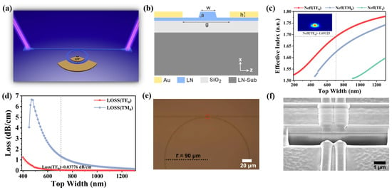
Figure 1.
Design of the microring resonator. (a) Device diagram, showing the optical fiber, grating coupler, microring resonator and electrodes. (b) Waveguide design of microring resonator. (c) Effective refractive index of waveguide modes at different top widths; the inset shows the mode of the waveguide at 1550 nm. (d) Losses of mode and mode for different top widths. (e) A partial SEM image of the microring resonator; the figure contains part of the line waveguide and the ring waveguide and the radius of the microring resonator is 90 m. (f) SEM cross-sectional image of the microring resonator coupling region, corresponding to the region in the red dashed box in (e).
Figure 1c,d show the calculated results of the mode field, effective refractive index and loss in the Finite Difference Eigenmode (FDE). With the chosen parameters, the microring resonator can transmit the mode near 1550 nm with less loss, achieving effective optical mode confinement and propagation. Focused grating couplers are designed at both ports of the microring resonator for laser input and output [33,34,35,36]. According to the simulation results, the focused grating couplers can achieve a transmittance (T) of 0.32, a 3 dB bandwidth of 120 nm and a maximum coupling efficiency () of 56.5% according to . They can provide optical power input and data output for experiments with our device.
Our device was fabricated from a commercially available x-cut LNOI wafer (NANOLN, Jinan Jingzheng Electronics Co., Ltd., Jinan, China), with a 400 nm LN layer, 2 m , on a 500 m LN substrate. The first part of the fabrication process consists of patterning the LN structures, including the grating couplers and the waveguide microring resonator. Electron-beam lithography (EBL) with hydrogen silsesquioxane (HSQ) resist followed by -based reactive ion etching (RIE, 250 nm etch depth) was used to pattern the optical layer of the device. The second part of the fabrication process consists of adding electrodes to the microring resonator. The device was cleaned and micro-wave electrodes (10 nm of Cr, 250 nm of Au) were deposited via photolithography followed by electron-beam evaporation and a lift-off process [11]. Figure 1e shows partial SEM images of the line waveguide and the circular portion of the microring resonator, whereas Figure 1f shows the SEM image of the waveguide cross-section in the coupling region and its position is pictured with a red dashed line in Figure 1e.
3. Characteristic Measurement and Results
The first part of the measurement was the spectrum of a passive microring resonator without metal electrodes. The experimental setup is shown in Figure 2a. A continuously tunable laser (YOKOGAWA AQ2200-136, 1440–1640 nm) emits laser light, which is collected by a single-mode fiber and coupled to a grating coupler to complete optical transmission from the laser to the device. After passing through the device, the optical signal was transmitted by a grating coupler at the other port to an optical fiber, which was then connected to an optical spectrum analyzer (YOKOGAWA AQ6370D, 600–1700 nm) for data collection. The laser and optical spectrum analyzer were connected via Labview software and the computer controlled the input and output of the optical signal as well as experimental data acquisition. We used DC Power supply (MCH K305D, 0–30 V) with a resolution of 0.1 V to apply the voltage to the pending measured device.
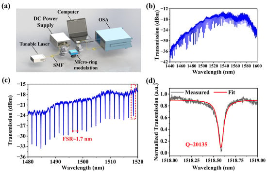
Figure 2.
Measurements of the spectrum without the addition of voltage. (a) Experimental measurement setup diagram. (b) The measurement range is from 1440 nm to 1600 nm. (c) Measurement results with improved accuracy in the range of 1480 nm to 1520 nm. (d) Enlargement of the red box in (c), Lorentz fit of the resonance line shape and calculation of the of approximately 20,315 at 1518.549 nm.
The measured spectra are shown in Figure 2b without any voltage applied and the measured range was from 1440 nm to 1600 nm. The resonance peaks are regularly spaced apart in the figure, indicating that only one major peak is excited in the microring resonator, which is likely owing to the same geometrical parameters of the line and ring waveguides. As shown in Figure 2c, we chose a region of the spectrum with better coupling effects in Figure 2b and improved the accuracy for the measurement, from 1480 nm to 1520 nm, and we measured the free spectral range (FSR) to be approximately 1.7 nm, with a maximum extinction ratio of approximately 11 dB. Figure 2d is an enlargement of the red dashed box in Figure 2c and we chose the peak at 1518.549 nm to obtain the value of the intrinsic optical quality factor (∼20,315) using the Lorentz equation. The extinction ratio of our microring resonator can be further enhanced if the cladding environment surrounding the LN waveguide is [27].
The modulation efficiency, which is the shift in the resonant wavelength when a certain voltage is applied, is the metric used to evaluate the performance of the microring modulator. The device structure shown in this paper was used for direct current (DC) electro-optical modulation by applying voltage to the device using a probe at the electrode. When a voltage is applied, the effective refractive index of the LN material changes and the alteration in the refractive index changes the effective optical range length of the resonator, resulting in a frequency shift of the resonance. A wavelength shift of the resonance with voltage is observed by sequentially adding the DC voltage from 0 V to +30 V and then reversing the voltage from 0 V to –30 V. The results of the experimental observations are shown in Figure 3c,d. The resonant wavelength exhibits a bathochromic shift following the addition of a DC positive voltage, whereas it exhibits a hypsochromic shift following the addition of a DC negative voltage.
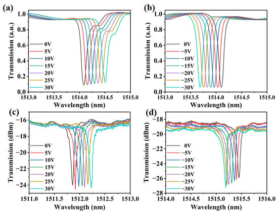
Figure 3.
Microring resonator DC electro-optical modulation. (a) Simulation results of adding positive voltage modulation. (b) Simulation results of adding negative voltage modulation. (c) Positive voltage modulation experimental spectrum. (d) Negative voltage modulation experimental spectrum.
According to the fitting shown in Figure 4, the measured average voltage modulation efficiency is 10.8 pm/V. The turning efficiency of the voltage reaches 13 pm/V when a positive voltage of 25 V to 30 V is applied to the device, which is slightly higher than the average voltage modulation efficiency. In contrast, when a negative voltage of –25 V to –30 V is applied, the turning efficiency is 4.2 pm/V, demonstrating the asymmetry between the positive and negative voltage modulation. The hypsochromic/bathochromic shift of the resonant wavelength persisted for a period of time after the DC bias voltage was removed. The difference in the degree of influence of the positive and negative voltages on the resonant wavelength shift was measured experimentally and the Maxwell–Wagner effect [27,37] found in the device was analyzed. That is, the asymmetry of the resonant wavelength shift under the influence of the static EO effect is due to the interfacial polarization phenomenon caused by the charge accumulation between the interface of the LN waveguide and the air cladding. Figure 3a,b, which are the results of the simulation, show the effects of the positive and negative voltage modulation of the device, respectively. Figure 4 is fitted with the modulation efficiency, which is 13.88 pm/V, which is compatible with our experimental results. Comparing the microring modulator based on LNOI or LN hybrid platforms to the other studies in Table 1, our modulator performs better than the other devices in terms of the compromise between chip size and modulation efficiency.
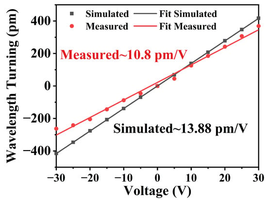
Figure 4.
Fitting results for the electro-optical modulation efficiency of the microring resonator, with the red and black lines representing the results of experimental measurement and simulation, respectively.

Table 1.
Comparison of the footprint and modulation efficiency of different LN microring modulators.
To study the impact of the resonant wavelength shift of the device under the modulation of square-wave signals of different amplitudes, a 1 KHz square wave signal was added to the device. Figure 5a depicts the experimental setup and the electrodes of the chip are loaded with a square-wave signal from the signal generator (SIGLMENT SDG2082X). Because the frequency of the added square wave-signal is much faster than the wavelength scan, two stable resonances appear at each square-wave signal of different pulse amplitudes, leading to retention effects in the spectrum, as shown in Figure 5b, where the two stable resonances are distributed on the left and right of the resonant wavelength, corresponding to the positive and negative voltages applied to the device. The resonant wavelength tunable bandwidth of the device can reach 17.5 GHz at a low pulse signal of 20 Vpp. Furthermore, as shown in Figure 5c, the square wave signal modulation results are fitted and an alternating current (AC) modulation efficiency of approximately 7.6 pm/V is obtained. This is consistent with our preconceived results that AC modulation efficiency is lower than the static voltage modulation efficiency.
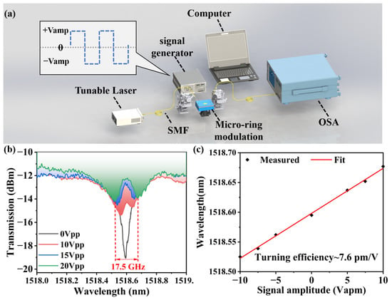
Figure 5.
AC electro-optical modulation of the microring resonator. (a) Diagram of the experimental measuring setup. The square wave signal is shown in the upper left corner. It has two states: +Vapm and -Vapm. (b) Experimental measurement spectra for square wave signals of different amplitudes. (c) Fitting outcomes for the modulation efficiency of the AC signal.
Because the modulation of the device is affected by temperature [42,43,44], we also verified the sensitivity of the device to ambient temperature. The device was heated at room temperature by placing a metal ceramic heater at the bottom of the chip from 30 C to 100 C and observing the spectrum at the light-emitting port. Figure 6a shows the wavelength shift results of the microring resonator after temperature modulation. It is experimentally shown that the resonant wavelength of the microring resonator is bathochromically shifted after every 10 C temperature increase. Figure 6b shows the fitted wavelength shift efficiency, with a resulting temperature modulation efficiency of 26.33 pm/C while producing almost no additional optical transmission loss. The chip can be adjusted for better efficiency and can accommodate a larger tunable range in the future under varied environmental sensitivity settings if it is co-modulated with voltage modulation and temperature modulation.
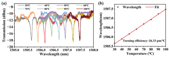
Figure 6.
Temperature modulation of the microring resonator. (a) Experimental spectral measurements showing the shift of the resonant peak when the temperature is raised in 10 C increments. (b) Efficiency of temperature modulation fitting results.
4. Discussion
The microring modulator we designed modifies the refractive index of by introducing an electric field, thereby changing the wavelength position of the resonant wavelength and achieving a tuning efficiency of 10.8 pm/V in the electric field range of –30 V∼+30 V with electrodes distancing 5 m. The electro-optical tuning rate can be further improved, such as designing racetrack resonators with electrodes, which are placed on both sides of the straight waveguide so that the applied DC field between the two electrodes is exactly in the extraordinary direction of the crystal, to take advantage of the maximum . In addition, a cladding can be used around the LN waveguide to match the high dielectric constant of the LN, which can enhance overlap, further enhance the tuning efficiency of the device and also improve the extinction ratio.
In addition to its other benefits, it should be noted that increasing the thickness of the electrode can further enhance electro-optic overlap and consequently improve the efficiency of tuning [38].
The scheme proposed in this paper is a versatile modulator based on a compact LN microring resonator, which can be applied in microring-based sensor arrays and integrated optics. Its subwavelength structure enhances the effect of light–matter interactions such as electro-optic and thermo-optic effects. Furthermore, this device provides a new solution for the ambient temperature compensation functional behavior of on-chip electro-optic modulators.
5. Conclusions
Based on X-cut LNOI, we designed a compact microring modulator with versatile tuning that achieved a maximum electro-optical tuning efficiency of 13 pm/V in a compact modulation platform at the micron stage. The asymmetry of positive and negative voltage tuning in static voltage modulation indicates that the Maxwell–Wagner effect is present in the device. With the addition of low-frequency pulse signal modulation, the device exhibts a modulation bandwidth of 17.5 GHz and an AC tuning efficiency of 7.6 pm/V. Additionally, the temperature control efficiency of the device was measured to be 26.33 pm/V, enabling the synergistic modulation of electrical modulation and temperature control in applications that are not temperature-sensitive in the near future. The modulator requires further exploration to achieve more functional tuning. The compact waveguide microring resonator that we fabricated is anticipated to be tightly combined with other on-chip active and passive components, adding a novel perspective to the development of future compact, effective and simply modulated communication systems.
Author Contributions
Conceptualization, Q.L. and H.L.; methodology, Y.H. and R.L.; software, Q.L., Y.L. and H.C.; formal analysis, H.L. and G.T.; data curation, T.Y., W.Q., H.G., Q.L. and H.C.; writing—review and editing, H.L.; visualization, Y.H. All authors have read and agreed to the published version of the manuscript.
Funding
This research was funded in part by the National Natural Science Foundation of China (61775084, 62075088), the NSAF (U2030103, U2230111), the Natural Science Foundation of Guangdong Province (2020A1515010791, 2021A0505030036, 2022A1515110970), the Fundamental and application foundation project of Guangzhou (202201010654), the Fundamental Research Funds for the Central Universities (21622107, 21622403), the Supported by the Outstanding Innovative Talents Cultivation Funded Programs for Doctoral Students of Jinan University (2022CXB011).
Institutional Review Board Statement
Not applicable.
Informed Consent Statement
Not applicable.
Data Availability Statement
The data that support the findings of this study are available from the corresponding author upon reasonable request.
Conflicts of Interest
The authors declare no conflict of interest.
References
- Powell, K.; Li, L.; Shams-Ansari, A.; Wang, J.; Meng, D.; Sinclair, N.; Deng, J.; Lončar, M.; Yi, X. Integrated silicon carbide electro-optic modulator. Nat. Commun. 2022, 13, 1851. [Google Scholar] [CrossRef] [PubMed]
- Jiang, Y.; Han, X.; Huang, H.; Zhang, P.; Dubey, A.; Xiao, H.; Yuan, M.; Frigg, A.; Nguyen, T.G.; Boes, A.; et al. Monolithic Photonic Integrated Circuit Based on Silicon Nitride and Lithium Niobate on Insulator Hybrid Platform. Adv. Photonics Res. 2022, 3, 2200121. [Google Scholar] [CrossRef]
- Xu, Q.; Schmidt, B.; Pradhan, S.; Lipson, M. Micrometre-scale silicon electro-optic modulator. Nature 2005, 435, 325–327. [Google Scholar] [CrossRef]
- Sun, C.; Wade, M.T.; Lee, Y.; Orcutt, J.S.; Alloatti, L.; Georgas, M.S.; Waterman, A.S.; Shainline, J.M.; Avizienis, R.R.; Lin, S.; et al. Single-chip microprocessor that communicates directly using light. Nature 2015, 528, 534–538. [Google Scholar] [CrossRef]
- Teng, M.; Fathpour, S.; Safian, R.; Zhuang, L.; Honardoost, A.; Alahmadi, Y.; Polkoo, S.S.; Kojima, K.; Wen, H.; Renshaw, C.K.; et al. Miniaturized Silicon Photonics Devices for Integrated Optical Signal Processors. J. Light. Technol. 2020, 38, 6–17. [Google Scholar] [CrossRef]
- Baehr-Jones, T.; Ding, R.; Liu, Y.; Ayazi, A.; Pinguet, T.; Harris, N.C.; Streshinsky, M.; Lee, P.; Zhang, Y.; Lim, A.E.; et al. Ultralow drive voltage silicon traveling-wave modulator. Opt. Express 2012, 20, 12014–120209. [Google Scholar] [CrossRef]
- Tu, X.; Liow, T.Y.; Song, J.; Luo, X.; Fang, Q.; Yu, M.; Lo, G.Q. 50-Gb/s silicon optical modulator with traveling-wave electrodes. Opt. Express 2013, 21, 12776–12782. [Google Scholar] [CrossRef]
- Wang, C.; Zhang, M.; Chen, X.; Bertrand, M.; Shams-Ansari, A.; Chandrasekhar, S.; Winzer, P.; Lončar, M. Integrated lithium niobate electro-optic modulators operating at CMOS-compatible voltages. Nature 2018, 562, 101–104. [Google Scholar] [CrossRef]
- Ahmed, A.N.R.; Nelan, S.; Shi, S.; Yao, P.; Mercante, A.; Prather, D.W. Subvolt electro-optical modulator on thin-film lithium niobate and silicon nitride hybrid platform. Opt. Lett. 2020, 45, 1112–1115. [Google Scholar] [CrossRef] [PubMed]
- Wang, T.J.; Chu, C.H.; Lin, C.Y. Electro-optically tunable microring resonators on lithium niobate. Opt. Lett. 2007, 32, 2777–2779. [Google Scholar] [CrossRef]
- Hu, Y.; Yu, M.; Zhu, D.; Sinclair, N.; Shams-Ansari, A.; Shao, L.; Holzgrafe, J.; Puma, E.; Zhang, M.; Loncar, M. On-chip electro-optic frequency shifters and beam splitters. Nature 2021, 599, 587–593. [Google Scholar] [CrossRef] [PubMed]
- Feng, H.; Zhang, K.; Sun, W.; Ren, Y.; Zhang, Y.; Zhang, W.; Wang, C. Ultra-high-linearity integrated lithium niobate electro-optic modulators. Photonics Res. 2022, 10, 2366. [Google Scholar] [CrossRef]
- Liu, H.-Y.; Shang, M.; Liu, X.; Wei, Y.; Mi, M.; Zhang, L.; Gong, Y.-X.; Xie, Z.; Zhu, S. Deterministic N-photon state generation using lithium niobate on insulator device. Adv. Photonics Nexus 2022, 2, 016003. [Google Scholar] [CrossRef]
- Shams-Ansari, A.; Yu, M.; Chen, Z.; Reimer, C.; Zhang, M.; Picqué, N.; Lončar, M. Thin-film lithium-niobate electro-optic platform for spectrally tailored dual-comb spectroscopy. Commun. Phys. 2022, 5, 88. [Google Scholar] [CrossRef]
- He, Y.; Yang, Q.-F.; Ling, J.; Luo, R.; Liang, H.; Li, M.; Shen, B.; Wang, H.; Vahala, K.; Lin, Q. Self-starting bi-chromatic LiNbO3 soliton microcomb. Optica 2019, 6, 1138–1144. [Google Scholar] [CrossRef]
- Lu, J.; Surya, J.B.; Liu, X.; Bruch, A.W.; Gong, Z.; Xu, Y.; Tang, H.X. Periodically poled thin-film lithium niobate microring resonators with a second-harmonic generation efficiency of 250,000%/W. Optica 2019, 6, 1455–1460. [Google Scholar] [CrossRef]
- Wang, C.; Zhang, M.; Yu, M.; Zhu, R.; Hu, H.; Loncar, M. Monolithic lithium niobate photonic circuits for Kerr frequency comb generation and modulation. Nat. Commun. 2019, 10, 978. [Google Scholar] [CrossRef]
- Gong, Z.; Shen, M.; Lu, J.; Surya, J.B.; Tang, H.X. Monolithic Kerr and electro-optic hybrid microcombs. Optica 2022, 9, 1060–1065. [Google Scholar] [CrossRef]
- Weis, R.S.; Gaylord, T.K. Lithium niobate: Summary of physical properties and crystal structure. Appl. Phys. A 1985, 37, 191–203. [Google Scholar] [CrossRef]
- Weber, M.J. Handbook of Optical Materials; CRC Press: Boca Raton, FL, USA, 2002. [Google Scholar]
- Zhang, M.; Wang, C.; Cheng, R.; Shams-Ansari, A.; Lončar, M. Monolithic ultra-high-Q lithium niobate microring resonator. Optica 2017, 4, 1536–1537. [Google Scholar] [CrossRef]
- He, Y.; Liang, H.; Luo, R.; Li, M.; Lin, Q. Dispersion engineered high quality lithium niobate microring resonators. Opt. Express 2018, 26, 16315–16322. [Google Scholar] [CrossRef] [PubMed]
- Krasnokutska, I.; Tambasco, J.J.; Li, X.; Peruzzo, A. Ultra-low loss photonic circuits in lithium niobate on insulator. Opt. Express 2018, 26, 897–904. [Google Scholar] [CrossRef] [PubMed]
- Zhou, J.-X.; Gao, R.-H.; Lin, J.; Wang, M.; Chu, W.; Li, W.-B.; Yin, D.-F.; Deng, L.; Fang, Z.-W.; Zhang, J.-H.; et al. Electro-Optically Switchable Optical True Delay Lines of Meter-Scale Lengths Fabricated on Lithium Niobate on Insulator Using Photolithography Assisted Chemo-Mechanical Etching. Chin. Phys. Lett. 2020, 37, 084201. [Google Scholar] [CrossRef]
- Bahadori, M.; Goddard, L.L.; Gong, S. Fundamental electro-optic limitations of thin-film lithium niobate microring modulators. Opt. Express 2020, 28, 13731–13749. [Google Scholar] [CrossRef]
- Li, K.; Wang, S.; Han, X.; Wang, Z. Dispersion Measurement of Electro-Optic Coefficient γ22 of Lithium Niobate Based on Photoelastic Modulation. Appl. Sci. 2020, 10, 395. [Google Scholar] [CrossRef]
- Bahadori, M.; Yang, Y.; Hassanien, A.E.; Goddard, L.L.; Gong, S. Ultra-efficient and fully isotropic monolithic microring modulators in a thin-film lithium niobate photonics platform. Opt. Express 2020, 28, 29644–29661. [Google Scholar] [CrossRef]
- Wang, T.-J.; Peng, G.-L.; Chan, M.-Y.; Chen, C.-H. On-Chip Optical Microresonators With High Electro-Optic Tuning Efficiency. J. Light. Technol. 2020, 38, 1851–1857. [Google Scholar] [CrossRef]
- Janner, D.; Tulli, D.; García-Granda, M.; Belmonte, M.; Pruneri, V. Micro-structured integrated electro-optic LiNbO3 modulators. Laser Photonics Rev. 2009, 3, 301–313. [Google Scholar] [CrossRef]
- Kai Xin, C.; Xue Peng, L.; Yan Lin, Z.; Kin Seng, C. Lithium-Niobate Mach-Zehnder Interferometer With Enhanced Index Contrast by SiO2 Film. IEEE Photonics Technol. Lett. 2015, 27, 1224–1227. [Google Scholar] [CrossRef]
- Wang, Y.; Zhou, S.; He, D.; Hu, Y.; Chen, H.; Liang, W.; Yu, J.; Guan, H.; Luo, Y.; Zhang, J.; et al. Electro-optic beam deflection based on a lithium niobate waveguide with microstructured serrated electrodes. Opt. Lett. 2016, 41, 4739–4742. [Google Scholar] [CrossRef] [PubMed]
- Pan, B.; Tan, Y.; Chen, P.; Liu, L.; Shi, Y.; Dai, D. Compact Racetrack Resonator on LiNbO3. J. Light. Technol. 2021, 39, 1770–1776. [Google Scholar] [CrossRef]
- Chen, Z.; Peng, R.; Wang, Y.; Zhu, H.; Hu, H. Grating coupler on lithium niobate thin film waveguide with a metal bottom reflector. Opt. Mater. Express 2017, 7, 4010–4017. [Google Scholar] [CrossRef]
- Nisar, M.S.; Zhao, X.; Pan, A.; Yuan, S.; Xia, J. Grating Coupler for an On-Chip Lithium Niobate Ridge Waveguide. IEEE Photonics J. 2017, 9, 6600208. [Google Scholar] [CrossRef]
- Kar, A.; Bahadori, M.; Gong, S.; Goddard, L.L. Realization of alignment-tolerant grating couplers for z-cut thin-film lithium niobate. Opt. Express 2019, 27, 15856–15867. [Google Scholar] [CrossRef] [PubMed]
- Krasnokutska, I.; Chapman, R.J.; Tambasco, J.J.; Peruzzo, A. High coupling efficiency grating couplers on lithium niobate on insulator. Opt. Express 2019, 27, 17681–17685. [Google Scholar] [CrossRef]
- Jinesh, K.B.; Lamy, Y.; Klootwijk, J.H.; Besling, W. Maxwell–Wagner instability in bilayer dielectric stacks. Appl. Phys. Lett. 2009, 95, 1858. [Google Scholar] [CrossRef]
- Ahmed, A.N.R.; Shi, S.; Mercante, A.J.; Prather, D.W. High-performance racetrack resonator in silicon nitride - thin film lithium niobate hybrid platform. Opt. Express 2019, 27, 30741–30751. [Google Scholar] [CrossRef]
- Mahmoud, M.; Cai, L.; Bottenfield, C.; Piazza, G. Lithium Niobate Electro-Optic Racetrack Modulator Etched in Y-Cut LNOI Platform. IEEE Photon. J. 2018, 10, 6600410. [Google Scholar] [CrossRef]
- Ahmed, A.N.R.; Shi, S.; Zablocki, M.; Yao, P.; Prather, D.W. Tunable hybrid silicon nitride and thin-film lithium niobate electro-optic microresonator. Opt. Lett. 2019, 44, 618–621. [Google Scholar] [CrossRef]
- Wang, C.; Zhang, M.; Stern, B.; Lipson, M.; Lončar, M. Nanophotonic lithium niobate electro-optic modulators. Opt. Express 2018, 26, 1547–1555. [Google Scholar] [CrossRef]
- Chen, J.-Y.; Sua, Y.M.; Fan, H.; Huang, Y.-P. Modal phase matched lithium niobate nanocircuits for integrated nonlinear photonics. OSA Contin. 2018, 1, 229–242. [Google Scholar] [CrossRef]
- Wang, J.Q.; Yang, Y.H.; Li, M.; Hu, X.X.; Surya, J.B.; Xu, X.B.; Dong, C.H.; Guo, G.C.; Tang, H.X.; Zou, C.L. Efficient Frequency Conversion in a Degenerate χ(2) Microresonator. Phys. Rev. Lett. 2021, 126, 133601. [Google Scholar] [CrossRef] [PubMed]
- Shi, X.; Fan, W.; Hansen, A.K.; Chi, M.; Yi, A.; Ou, X. Thermal Behaviors and Optical Parametric Oscillation in 4H-Silicon Carbide Integrated Platforms. Adv. Photonics Res. 2021, 2, 2100068. [Google Scholar] [CrossRef]
Disclaimer/Publisher’s Note: The statements, opinions and data contained in all publications are solely those of the individual author(s) and contributor(s) and not of MDPI and/or the editor(s). MDPI and/or the editor(s) disclaim responsibility for any injury to people or property resulting from any ideas, methods, instructions or products referred to in the content. |
© 2023 by the authors. Licensee MDPI, Basel, Switzerland. This article is an open access article distributed under the terms and conditions of the Creative Commons Attribution (CC BY) license (https://creativecommons.org/licenses/by/4.0/).