Communication

High-Efficiency Integrated Color Routers by Simple Identical Nanostructures for Visible and Near-Infrared Wavelengths

State Key Laboratory of Optoelectronic Materials and Technologies, School of Physics, Sun Yat-sen University, Guangzhou 510275, China
*
Author to whom correspondence should be addressed.
Photonics 2023, 10(5), 536; https://doi.org/10.3390/photonics10050536
Submission received: 4 April 2023 / Revised: 28 April 2023 / Accepted: 4 May 2023 / Published: 6 May 2023
(This article belongs to the Special Issue Micro-Nano Optical Devices)

Abstract

:
Imaging in both the visible and the near-infrared ranges has various applications in computational photography and computer vision. Comparing it with the traditional imaging system, integrating pixel-level metasurfaces on the imaging sensor is effective to plot the route of visible and near-infrared light to the right pixels, while the previously reported nanostructures were complicated to design and fabricate. Here, a pixel-level color router based on metalens, which provides a much simpler construction to improve the visible and near-infrared imaging efficiencies to 59% and 60%, is designed.

1. Introduction

Visible light cameras have been widely used in daily life. However, the useful information at the near-infrared (NIR) wavelengths is lost due to the weak detection ability of the imaging sensor. Therefore, imaging from the visible to NIR wavelengths is of significance to many applications. As an example of computer vision, facial recognition by the visible light is vulnerable to the ambient light, while NIR light can correct this shortcoming [1,2,3,4]. The NIR light also has stronger penetration and smaller scattering of the air particles than the visible light. Hence, the fusion of visible and NIR light can be used for weak-light imaging [5,6,7,8,9,10,11].
Traditional imaging systems usually require two separated optical configurations to capture the visible and NIR light, respectively, making the systems large, expensive and complex. In addition, adding color filters on the imaging sensors will reduce the energy by more than 50%. These problems can be resolved by integrating pixel-level metasurface-based color routers. This kind of color router deflects different colors of light to different pixels of the imaging sensor. It can achieve a light collection efficiency of more than 45%, which represents the light collection efficiency limitation of the conventional color filter with a transmission of 90%, thereby improving the imaging quality and contributing to the development of sensor miniaturization. Metasurfaces, which consist of arrays of artificially fabricated nanostructures, have the prominent ability to control the electromagnetic wave properties for desired functions [12,13,14,15,16,17]. The Metasurface-based color routers can orient the light rather than filtering it, which effectively increases the imaging efficiency [18,19,20,21,22,23,24,25,26]. However, the previously reported color metasurface-based routers suffer from having complicated structures, posing high accuracy requirement for their fabrication [19,20,21,22,23,24,25,26,27,28].
In order to overcome the aforementioned problems, a pixel-level color router based on a metalens is designed. This structure can simultaneously achieve efficient visible and NIR imaging on the same imaging sensor, while the nanostructures are relatively simple. The concept is illustrated in Figure 1. This thin film device can direct the visible (400–700 nm) and NIR (700–1100 nm) light into different pixels with a collection efficiency of 59% and 60%, which is higher than the 45% of the conventional color filters. Furthermore, the unit cells of our color routers are only composed of identical silicon-nitride nanopillars with a side length of 180 nm and a height of 800 nm, which is much simpler than the former pixel-level and metasurface-based color routers. This work provides a new design guideline for a single imaging sensor to achieve convenient and high-quality visible-NIR images.

2. Design Methods

In order to achieve pixel-level color routing, the target phase profile of the metalens was calculated. As shown in Figure 1, the visible and NIR light were directed and focused to the corresponding pixels by an array of periodic metalenses. Each metalens had a size of 4 μm × 4 μm to cover four square pixels. The metalens is centrally symmetrical and encodes two hyperbolic phase profiles for the visible and NIR light, respectively:
φ 650   nm ( x , y ) = 2 π λ 650   nm n ( f 2 + ( x x 650   nm ) 2 + ( y y 650   nm ) 2 f ) + C 650   nm
φ 860   nm ( x , y ) = 2 π λ 860   nm n ( f 2 + ( x x 860   nm ) 2 + ( y y 860   nm ) 2 f ) + C 860   nm
where 650 nm and 860 nm represent the working wavelength of visible and NIR light, respectively. The boundary of the metalens is shown in Figure 1. The focal length of the metalens was f = 4 μm; C650nm = 1 and C860nm = 4.1 are constants related to the reference phases for the wavelength of 650 nm and 860 nm, which are tuned to match the phase of the meta-atoms to the phase profiles and can be obtained according to Ref. [22] (x650nm, y650nm) and (x860nm, y860nm) denote the focal points on the visible pixel and the NIR pixel, respectively. Then, FDTD Solutions (Lumerical Inc. from Canada.), a commercial software, was used to construct a phase library of meta-atoms to match the phase profile of the metalens.

3. Results

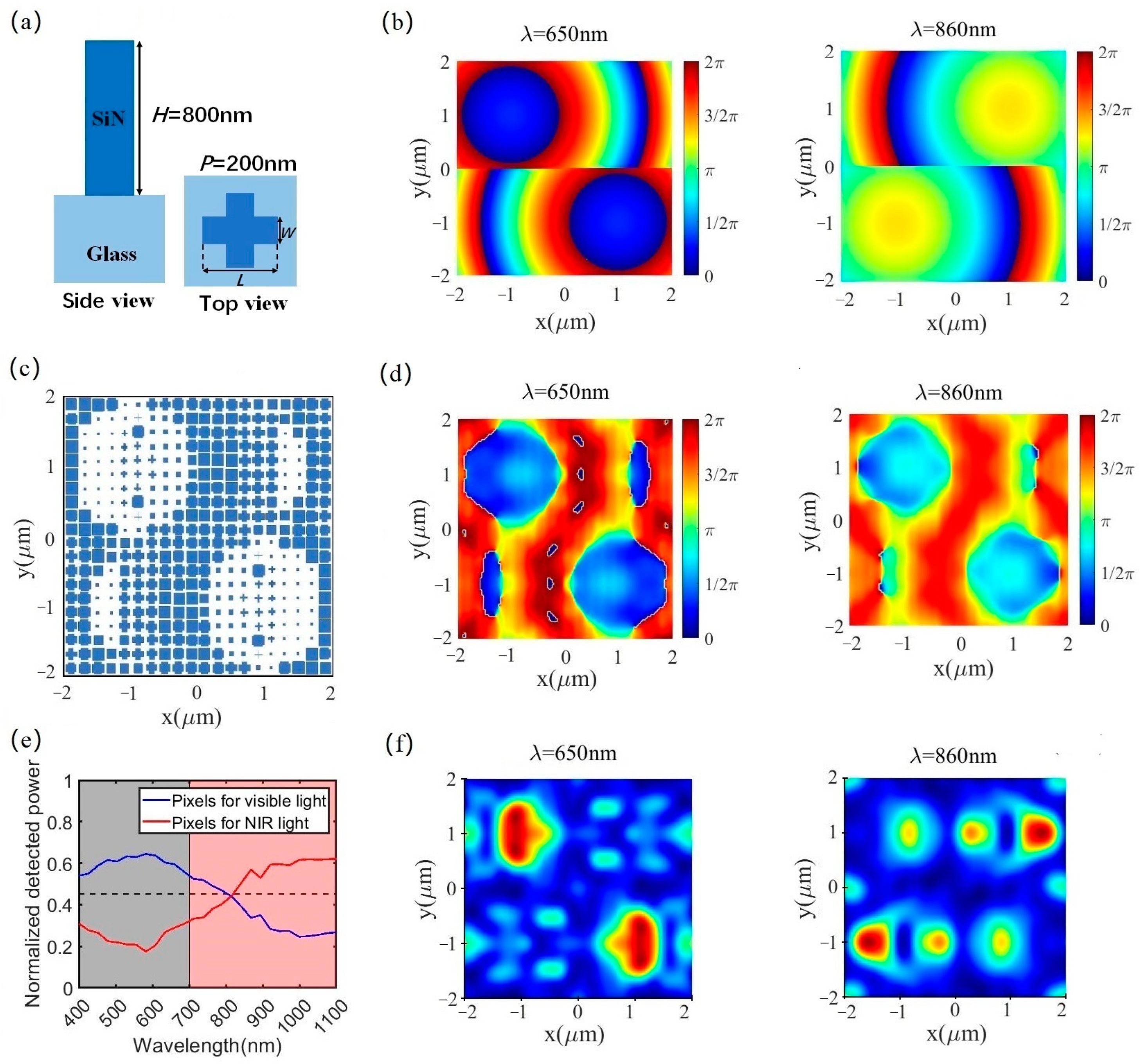
As shown in Figure 2a, the cross-shape nanopillars of silicon nitride with a height of H = 800 nm were used as the meta-atoms, which have accurate phase control and high transmission from the visible to NIR wavelengths. The period of the meta-atom was set to be P = 200 nm. The variation ranges of their lengths L and widths W were from 0.1P to 0.9P and from 0.1P to P, respectively. The corresponding theoretical phase distribution diagram is shown in Figure 2b. According to this theoretical phase distribution, we matched specific meta-atoms from the phase library in order to obtain the design structure, as shown in Figure 2c. The calculated output phases for the wavelengths of 650 nm and 860 nm are, respectively, shown in Figure 2d, which show distribution congruence with the theoretical results in Figure 2b.
Finally, the focusing performance of the metalens for the broadband normal incident light ranging from 400 nm to 1100 nm was also simulated. The light collection efficiency, defined as the ratio of the transmitted light into the corresponding pixel to the total incident light, was used to characterize the performance of the color router. Figure 2e shows the results of light routing. The blue and red lines represent the light collection efficiency of the imaging pixels for the visible and NIR light. The corresponding average light collection efficiencies were 60% and 52% for the visible and NIR light, respectively. Both results are higher than the dotted line in Figure 2e with a value of 45%. The point spread functions (PSFs) of the wavelengths at 650 nm and 860 nm on the same focal plane were also calculated by FDTD simulation and shown in Figure 2f. The results indicate that the proposed metalens can effectively direct the corresponding light to the targeted pixels.
Unlike the traditional metalens, there is no need for the color router to focus the light while it is only required to direct light energy to the corresponding pixels to the maximum extent. Therefore, in order to simplify the nanostructures, the further following optimization was performed:
(1)
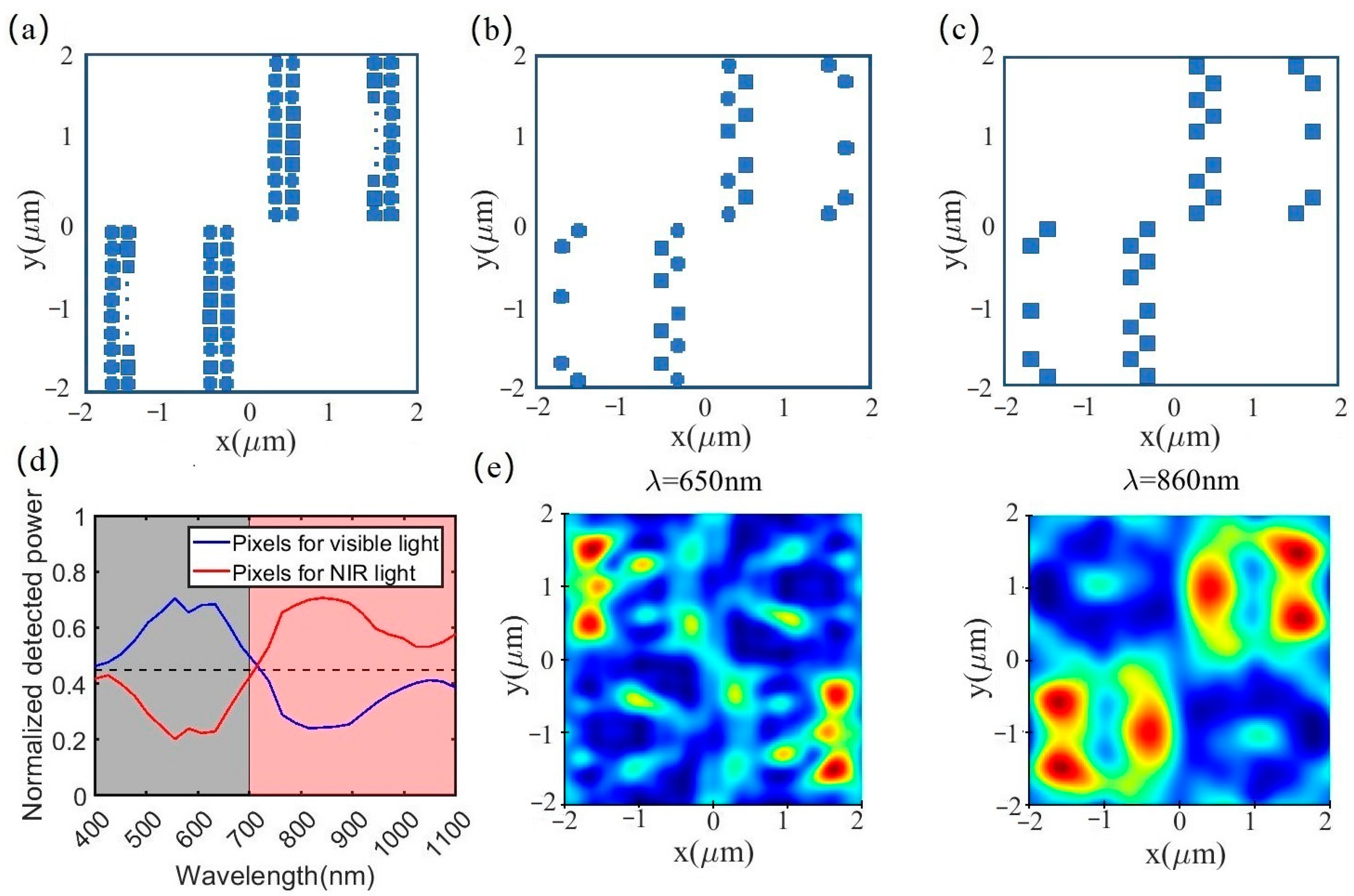
The columns of meta-atoms in the metalens in Figure 2c were eliminated as much as possible, while keeping the high average light collection efficiencies for the visible and NIR light to the corresponding imaging pixels. The remaining meta-atoms are illustrated in Figure 3a.
(2)
Furthermore, the meta-atoms with very small featured sizes (<40 nm) were eliminated due to their difficulty in fabrication. The remaining adjacent meta-atoms were also eliminated to reduce the near-field coupling. As the square-shape meta-atoms were easier to fabricate than the cross-shape ones, the square-shape meta-atoms were left alone to the greatest extent during the process, as shown in Figure 3b.
(3)
To further reduce the difficulty of the fabrication, the rest of the cross-shaped nanopillars were replaced with the same square-shape nanopillars, which had similar phases. Figure 3c shows the final structure of the optimized metalens. The side length of the square-shape nanopillars was 180 nm and the height was 800 nm.
Figure 3d shows the routing results of the simplified color router, which validates its effective performance. Figure 3e shows the light-field distribution of the visible and NIR light at the corresponding imaging pixels. Table 1 shows the light collection efficiency for each optimized step. It is clearly shown in Figure 2 that optimization maintains the light routing performance very effectively at the metalens, while achieving much simpler nanostructures and greatly reducing the fabricating difficulty. It can be seen that the obtained efficiency is slightly higher than the efficiency before optimization, which denotes that optimization effectively matches the light collection characteristics of the visible and NIR spectrum.
The tolerance of the incident angle on an imaging sensor determines the light routing quality. Hence, the average collection efficiency of our color router with different incident angles for the visible and NIR light was calculated and is shown in Figure 4 and Table 2. They show that the light collection efficiency stays higher than 50% of the normal incidence [22] when the incident angle is less than 35°, indicating that the tolerant range of the incident angle is about ±35°. Here, the maximum tolerance incident angle is defined as the angle when the efficiency drops to half of the normal incidence efficiency [22].

4. Discussion

The meta-atoms that make up the metalens structure have rotational symmetry. Hence, the color router is polarization-insensitive, providing a much simpler construction and improved efficiency for visible and NIR imaging. As shown in Table 3, compared to previously reported metasurface-based color routers, our new design employs a much simpler nanostructure for fabrication by electron beam lithography and dry etching [19,20,21,22,25,28]. Our design method is versatile and can be applied when modifying the pixel size of the imaging sensor. However, when the pixel size is too small, the range of available sizes is insufficient to accommodate a sufficient number of meta-atoms for an effective color router. As a result, the performance is compromised when the pixels are too small. Therefore, a larger pixel size would be more favorable for achieving better results, e.g., larger average collection efficiencies at an oblique incidence.

5. Conclusions

In summary, a pixel-level metalens-based color router is proposed to effectively orient the visible and NIR light into the corresponding imaging pixels with high collection efficiencies of 59% and 60%, respectively. Unlike the previously reported integrating color router based on complex nano-structures, this color router only composes of a series of identical silicon-nitride nanopillars with the same size. Hence, it greatly reduces the difficulty of fabrication. Furthermore, it has a wide tolerant range of ±35° for the incidence angle. This color design is anticipated to have the potential to increase the imaging quality for imaging sensors by improving the collecting efficiency for both the visible and NIR light.
In essence, this design method is a highly efficient and reliable technique for imaging both color and NIR images of a given scene simultaneously. It can be extended to the creation of RGB-NIR four-color channel color routers, which can be used to capture high-quality images in both color and NIR. With the growing demand for advanced imaging systems, the use of this design method is likely to become increasingly widespread in the years to come.

Author Contributions

H.L. and J.L. conceived the idea of the paper; R.Z., X.X. and Y.Z. did the calculations; R.Z., H.L. and J.L. wrote the manuscript. All authors contributed to the analysis of the results. All authors have read and agreed to the published version of the manuscript.

Funding

Guangdong Major Project of Basic and Applied Basic Research Foundation (2020B0301030009), National Natural Science Foundation of China (12074444, 11704421), Guangdong Basic and Applied Basic Research Foundation (2020B1515020019).

Institutional Review Board Statement

Not applicable.

Informed Consent Statement

Not applicable.

Data Availability Statement

Data is contained within the article.

Conflicts of Interest

The authors declare no conflict of interest.

References

  1. Jiang, F.; Liu, P.; Shao, X.; Zhou, X. Face anti-spoofing with generated near-infrared images. Multimed Tools Appl. 2020, 79, 21299–21323. [Google Scholar] [CrossRef]
  2. Jiang, F.; Liu, P.; Zhou, X. Multilevel fusing paired visible light and near-infrared spectral images for face anti-spoofing. Pattern Pecognit. Lett. 2019, 128, 30–37. [Google Scholar] [CrossRef]
  3. Prasad, M.S.; Shashanka, V.; Soma, B. Dictionary Alignment With Re-Ranking for Low-Resolution NIR-VIS Face Recognition. IEEE Trans. Inf. Forensic Secur. 2019, 14, 886–896. [Google Scholar]
  4. Raghavendra, R.; Dorizzi, B.; Rao, A.; Kumar, G.H. Particle swarm optimization based fusion of near infrared and visible images for improved face verification. Pattern Recogn. 2011, 44, 401–411. [Google Scholar] [CrossRef]
  5. Son, C.; Zhang, X. Near-Infrared Fusion via Color Regularization for Haze and Color Distortion Removals. IEEE Trans. Circuits Syst. Video Technol. 2018, 28, 3111–3126. [Google Scholar] [CrossRef]
  6. Xu, L.; Liang, P.; Han, J.; Bai, L.; Chen, D.Z. Global Filter of Fusing Near-Infrared and Visible Images in Frequency Domain for Defogging. IEEE Signal Process. Lett. 2022, 29, 1953–1957. [Google Scholar] [CrossRef]
  7. Awad, M.; Elliethy, A.; Aly, H.A. Adaptive Near-Infrared and Visible Fusion for Fast Image Enhancement. IEEE Trans. Comput. Imaging 2020, 6, 408–418. [Google Scholar] [CrossRef]
  8. Yuan, Y.; Shen, Y.; Peng, J.; Wang, L.; Zhang, H. Defogging Technology Based on Dual-Channel Sensor Information Fusion of Near-Infrared and Visible Light. J. Sens. 2020, 2020, 8818650. [Google Scholar] [CrossRef]
  9. Kanan, K.W.; Kishorjit, N.; Dinamani, S.A. Enhancing scene perception using a multispectral fusion of visible-near infrared image pair. IET Image Process. 2019, 13, 2467–2479. [Google Scholar]
  10. Hyuk-Ju, K.; Sung-Hak, L. Visible and Near-Infrared Image Acquisition and Fusion for Night Surveillance. Chemosensors 2021, 9, 75. [Google Scholar]
  11. Zhou, K.; Jung, C.; Yu, S. Scale-Aware Multispectral Fusion of RGB and NIR Images Based on Alternating Guidance. IEEE Access 2020, 8, 173197–173207. [Google Scholar] [CrossRef]
  12. Qin, J.; Jiang, S.; Wang, Z.; Cheng, X.; Li, B.; Shi, Y.; Tsai, D.P.; Liu, A.Q.; Huang, W.; Zhu, W. Metasurface Micro/Nano-Optical Sensors: Principles and Apprications. ACS Nano 2022, 16, 11598–11618. [Google Scholar] [CrossRef] [PubMed]
  13. Mansouree, M.; Kwon, H.; Arbabi, E.; McClung, A.; Faraon, A.; Arbabi, A. Multifunctional 2.5D metastructures enabled by adjoint optimization. Optica 2019, 7, 77–84. [Google Scholar] [CrossRef]
  14. Abdelraouf, O.A.M.; Wang, Z.; Liu, H.; Dong, Z.; Wang, Q.; Ye, M.; Wang, X.R.; Wang, Q.J.; Liu, H. Recent Advances in Tunable Metasurfaces: Materials, Design and Applications. ACS Nano 2022, 16, 13339–13369. [Google Scholar] [CrossRef]
  15. Deng, Y.; Cai, Z.; Ding, Y.; Bozhevolnyi, S.I.; Ding, F. Recent progress in metasurface-enabled optical waveplates. Nanophotonics 2022, 11, 2219–2244. [Google Scholar] [CrossRef]
  16. Yang, J.; Gurung, S.; Bej, S.; Ni, P.; Lee, H.W.H. Active optical metasurfaces: Comprehensive review on physics, mechanisms, and prospective applications. Rep. Prog. Phys. 2022, 85, 036101. [Google Scholar] [CrossRef]
  17. Guo, L.; Hu, Z.; Wan, R.; Long, L.; Li, T.; Yan, J.; Lin, Y.; Zhang, L.; Zhu, W.; Wang, L. Design of aluminum nitride metalens for broadband ultraviolet incidence routing. Nano Photonics 2019, 8, 171–180. [Google Scholar] [CrossRef]
  18. Zang, X.; Dong, F.; Yue, F.; Zhang, C.; Xu, L.; Song, Z.; Chen, M.; Chen, P.-Y.; Buller, G.S.; Zhu, Y.; et al. Polarization Encoded Color Image Embedded in a Dielectric Metasurface. Adv. Mater. 2018, 30, 1707499. [Google Scholar] [CrossRef]
  19. Chen, B.H.; Wu, P.C.; Su, V.-C.; Lai, Y.-C.; Chu, C.H.; Lee, I.C.; Chen, J.-W.; Chen, Y.H.; Lan, Y.-C.; Kuan, C.-H.; et al. GaN Metalens for Pixel-Level Full-Color Routing at Visible Light. Nano Lett. 2017, 17, 6345–6352. [Google Scholar] [CrossRef] [PubMed]
  20. Zou, X.; Zhang, Y.; Lin, R.; Gong, G.; Wang, S.; Zhu, S.; Wang, Z. Pixel-level Bayer-type colour router based on metasurfaces. Nat. Commun. 2022, 13, 3288. [Google Scholar] [CrossRef]
  21. Li, J.; Zhang, Q.; Yang, H.; Lei, T.; Du, L.; Wang, X.; Bu, J.; Chen, Q.; Liu, Y.; Xie, Z.; et al. Single-Layer Bayer Metasurface via Inverse Design. ACS Photonics 2022, 9, 2607–2613. [Google Scholar] [CrossRef]
  22. Miyata, M.; Nemoto, N.; Shikama, K.; Kobayashi, F.; Hashimoto, T. Full-color-sorting metalense for high-sensitivity image sensors. Optica 2021, 8, 1596–1604. [Google Scholar] [CrossRef]
  23. Zhao, N.; Catrysse, P.; Fan, S. Perfect RGB-IR Color Routers for Sub-Wavelength Size CMOS Image Sensor Pixels. Adv. Photonics Res. 2021, 2, 2000048. [Google Scholar] [CrossRef]
  24. Ballew, C.; Roberts, G.; Zheng, T.; Faraon, A. Constraining Continuous Topology Optimizations to Discrete Solutions for Photonic Applications. ACS Photonics 2023, 10, 836–844. [Google Scholar] [CrossRef] [PubMed]
  25. Zou, X.; Gong, G.; Lin, Y.; Fu, B.; Wang, S.; Zhu, S.; Wang, Z. Metasurface-based polarization color routers. Opt. Lasers Eng. 2023, 163, 107472. [Google Scholar] [CrossRef]
  26. Camayd-Muñoz, P.; Ballew, C.; Roberts, G.; Faraon, A. Multifunctional volumetric meta-optics for color and polarization image sensors. Optica 2020, 7, 280–283. [Google Scholar] [CrossRef]
  27. Catrysse, P.B.; Zhao, N.; Jin, W.; Fan, S. Subwavelength Bayer RGB color routers with perfect optical efficiency. Nanophotonics 2022, 11, 2381–2387. [Google Scholar] [CrossRef]
  28. Chang, K.-H.; Chen, Y.-C.; Huang, Y.-S.; Hsu, W.-L.; Lu, G.-H.; Liu, C.-F.; Weng, C.-J.; Lin, Y.-H.; Chen, C.-C.; Lee, C.-C.; et al. Axicon metalens for broadband light harvesting. Nanophotonics 2023, 12, 1309–1315. [Google Scholar] [CrossRef]
Figure 1. Sketch of the operating principle. The gray and red squares represent the pixels of the imaging sensor for the visible and NIR light, respectively. The size of the pixels is 2 µm × 2 µm. The (a) visible (white dashed lines) and (b) NIR (purple dashed lines) light are sorted and focused in the corresponding pixels by the color router on the front of the imaging sensor. The black dashed line represents one repeatable metalens as the color router.
Photonics 10 00536 g001
Figure 2. (a) Schematics of meta-atom with silicon nitride cross-shape nanopillar on glass. (b) The theoretical phase required for the metalens at a wavelength of 650 nm and 860 nm. (c) Structure of the metalens by obtaining the theoretical phase of (b), with a size of 4 μm × 4 μm. (d) The calculated phase of the metalens at a wavelength of 650 nm and 860 nm. (e) The light collection efficiency of the metalens. The dotted line represents the collection efficiency limitation of the conventional color filter with a transmittance of 90%. The gray and red regions represent the wavelength range of visible and NIR light, respectively. (f) The calculated PSFs of the metalens on the same focal plane at a wavelength of 650 nm and 860 nm.
Photonics 10 00536 g002
Figure 3. Structure of the color router after (a) step 1, (b) step 2, and (c) step 3 of the optimization. (d) The light collection efficiency of the final optimized color router (Figure 3c). The dotted line represents the collection efficiency limitation of the conventional color filter with a transmittance of 90%. The gray and red regions represent the wavelength range of visible and NIR light, respectively. (e) The corresponding calculated PSFs of the color router on the same focal plane at a wavelength of 650 nm and 860 nm.
Photonics 10 00536 g003
Figure 4. The normalized average collection efficiencies for the visible and NIR light at different incident angles. The dashed line indicates a collection efficiency of 50%.
Photonics 10 00536 g004
Table 1. The calculated average light collection efficiencies for the visible and NIR light to the corresponding imaging pixels during the optimization process.
StepFor Visible LightFor NIR Light
158%53%
258%60%
359%60%
Table 2. The normalized averages of light collection efficiencies for the visible and NIR light at different incident angels.
AngleFor Visible LightFor NIR Light
011
100.630.67
200.630.69
300.760.69
400.430.39
500.160.14
Table 3. Summary of metasurface-based color routers for imaging sensors.
ReferencesMaterialHeight of the
Nanostructures (nm)
Minimum Size
of Nanostructures (nm)
Working Wavelength
Range (nm)
Ref. [19]GaN60050400–1000
Ref. [20]Si3N4600125400–700
Ref. [21]TiO230080380–780
Ref. [22]Si3N41250≤100400–700
Ref. [25]Si3N4600100400–700
Ref. [28]TiO2150≤100450–900
This workSi3N4800180400–1100
Disclaimer/Publisher’s Note: The statements, opinions and data contained in all publications are solely those of the individual author(s) and contributor(s) and not of MDPI and/or the editor(s). MDPI and/or the editor(s) disclaim responsibility for any injury to people or property resulting from any ideas, methods, instructions or products referred to in the content.