Article

Wafer Eccentricity Deviation Measurement Method Based on Line-Scanning Chromatic Confocal 3D Profiler

1
Anhui Institute of Optics and Fine Mechanics, Hefei Institutes of Physical Science, Chinese Academy of Sciences, Hefei 230031, China
2
Science Island Branch, Graduate School of University of Science and Technology of China, Hefei 230026, China
3
Key Laboratory of Optical Calibration and Characterization of Chinese Academy of Sciences, Hefei 230031, China
*
Authors to whom correspondence should be addressed.
Photonics 2023, 10(4), 398; https://doi.org/10.3390/photonics10040398
Submission received: 15 February 2023 / Revised: 17 March 2023 / Accepted: 30 March 2023 / Published: 3 April 2023
(This article belongs to the Special Issue Recent Advances in Optical Metrology)

Abstract

:
The wafer eccentricity deviation caused by misalignment between the center of the wafer and rotary table will lead to edge image distortion and quality degradation of the defect signals during automated inspection. However, wafer end jump and edge topography change will bring great challenges to the accurate measurement of micrometer deviations. A new wafer eccentricity deviation measurement method based on line-scanning chromatic confocal sensors (LSCCSs) is proposed. Firstly, the LSCCS with Z-axis submicron resolution used in the experiment acquires the 3D profile height of the wafer edge as the turntable rotates, and the edge distance is calculated at each rotation angle. Secondly, a robust Fourier-LAR fitting method is used to fit edge distance serial to reduce sensitivity to outliers. Finally, the wafer eccentricity deviation that is equal to the wafer center coordinate can be calculated using the wafer eccentricity deviation model. In the simulated experiment, the results show that the eccentricity deviation measurement accuracy was insensitivity to noise and reached the micron level. Additionally, the measurement uncertainty of eccentricity deviation coordinate X w , Y w was (0.53 µm, 1.4 µm) in the actual data of the 12-inch wafers.

1. Introduction

As the degree of integration of semiconductor chips becomes higher and higher, the wafer size increases continuously and the lithography linewidth decreases gradually. Cutting-edge technology has pushed the processes below 7 nm, which puts forward higher requirements for the wafer surface and edge quality [1,2]. Sub-micron defects, such as scratches, particles, and residues on the wafer surface will seriously affect the subsequent grinding and coating process quality, resulting in wafer scraps. Automated wafer defect inspection technology for quality control has been widely studied and applied in the production lines [3,4,5,6].
Several detection approaches for wafer defects such as scanning electron microscopy (SEM), atomic force microscopy (AFM), and the photo-thermal reflectance technique have been proposed [7,8,9,10]. Although these methods have good sensitivity and resolution, their long detection times limit their application. Until now, the most common detection technology is the zoom microscope based on the dark-field scattering technique for micrometer-level defects. However, as the size of defects decreases to sub-micrometers, the sensitivity and ability to distinguish the defects are limited and cannot meet the detection requirements [11].
The spot laser scanning approach-based dark-field scattering technique for defect detection is faster and more accurate than the traditional imaging method [12], which has been widely applied in the famous semiconductor equipment manufacturer KLA’s products [13]. The wafer defect detection systems based on spot scanning generally use a single-wavelength laser as the incident light source to collect the scattering or reflection signals of the laser and process them to obtain a gray image. Then, the gray-scale image is analyzed to achieve the defect detection target. The method has high sensitivity to the defects (such as particles, scratches, and angular bumps) and has a good detection ability. However, the spot scanning detection approach is sensitive to the eccentricity errors of the wafer inspection system caused by misalignment between the wafer center and the turntable center. The eccentricity error will lead the wafer surface to produce a blind area, resulting in serious distortions in the image reconstruction and destruction of image integrity. Likewise, eccentricity error leads to defocus for the edge defect inspection, which will decrease the intensity of the defect signal. Hence, the eccentricity deviation error measurement is extremely important for wafer defect inspection.
There are two kinds of methods for wafer eccentricity detection and correction. One is the real-time hardware detection of the wafer edge with multiple locators to calculate the center of the wafer and then correct it. The patent describes three positioning heads to obtain the coordinates of the wafer edge points [13]. The center of the wafer is calculated through the processor, and the eccentric movement is carried out. This method requires high requirements for real-time acquisition and signal synchronization of multiple positioning heads and is vulnerable to the changes in wafer mark gaps and wafer defect pits.
The other is the acquisition of the image and the calibration of the calibration plate to calculate the deviation of the characteristic pattern to estimate the eccentricity. Additionally, the linear calibration object with specific characteristics is used for scanning in a previous work [12]. The image characteristics are reconstructed and the linear distortion is compensated using the calibration model. This method is complex and greatly affected by the accuracy of the calibration object. This method is not suitable for wafer edge inspection because of its curved appearance and difficult calibration. Meng et al. proposed a novel circle center location method for large-scale wafers [14]. The method measured the system angle in the horizontal plane. Through the analysis of multiple error sources and the compensation of system angle, a new hierarchical Bayesian model was utilized to estimate the circle center and radius and the average absolute deviation of the wafer circle parameter was within 0.12 mm.
3D measurement technology has been widely studied and successfully applied in many fields [15,16,17,18]. The line-scanning chromatic confocal sensor (LSCCS) is a device used to determine the surface distance of the measured object using light radiation [19]. The complex light dispersion emitted by the transmitter of the sensor is converted into a continuous wavelength spectrum. The wavelength is accurately mapped to the measured object by color coding. By measuring the wavelength of the highest intensity of the reflected light, the corresponding relationship between the sensor distance and the wavelength is established to obtain the position information of the measured object. The spectral confocal line sensor has the limitation of a fixed working distance range, and the depth of field is also small. However, the measurement accuracy of the Z-axis direction can reach the submicron level, which has high measurement accuracy and strong environmental adaptability. It is commonly used for 3D surface profile analysis and 3D size measurements [20,21,22,23], and can also be used for the measurement of the edge distance of the wafer.
To address the above issues, a wafer eccentricity deviation error measurement method based on line-scaling chromatic confocal sensors is proposed in this paper. The measurement system which can quickly acquire 3D profile information of the wafer edge and calculate the edge distance is described in Section 3.2. A robust Fourier-LAR fitting method is used to fit edge distance to reduce sensitivity to outliers. Then, the wafer eccentricity deviation which is equal to the wafer center coordinate, can be calculated by the circle fitting model.

2. Principle of Wafer Defect Inspection and Error Measurement

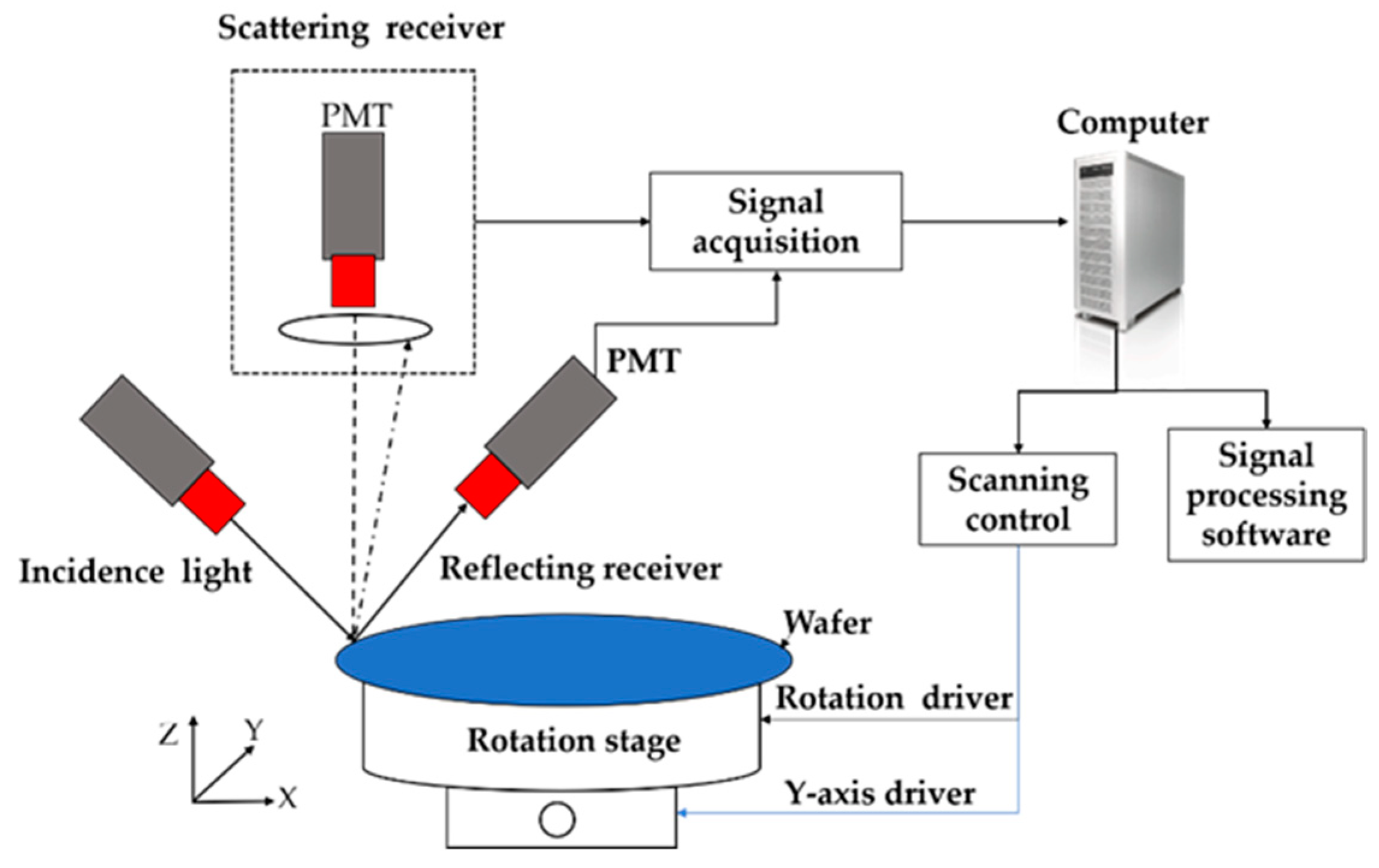
2.1. Spot Scanning Wafer Surface Defect Inspection and Wafer Eccentricity Deviation Error

The common detection approaches for detecting small defects are based on dark-field scattering technology that has high sensitivity. Figure 1 presents the layout of a spot scanning inspection system for wafer surface defects. The system directs a laser beam of radiation on the wafer surface, and then collects light reflected and scattered from the surface to identify defects such as particles, scratches, etc.
The illumination subsystem is configured to direct the layer beam of light to the wafer surface at an oblique angle of incidence. The collection subsystem includes two collection channels, which are arranged at different angles for collecting light scattered and light reflected from the specimen. A high sensitivity detector is essential to convert light collected into an electrical signal and increase the signal-to-noise ratio. Multiple types of detectors (such as phototubes and photomultiplier tube PMTs, etc.) can be selected.
A position subsystem that includes a two-dimensional translation stage and a rotation stage was designed for scanning the entire wafer surface. The position system is controlled by a computer and then the scattered and reflected signals are detected using a data acquisition card in real time. According to the obtained data points and scanning spiral trace, an entire wafer surface defect image can be finally constructed for further analysis.
For the wafer surface defect inspection, the ideal spot scanning process should ensure that the original scanning point position coincides with the rotation center of the spin mechanism. However, there is often a relative deviation between the two positions as shown in Figure 2, which will result in eccentric errors of the system in the motion process. Eccentric errors can cause serious distortion of the reconstructed wafer surface image and make the reconstructed image lose the ability to describe defect information, which has been illustrated in a previous work [10].
The heights of different positions on the detection focal plane are different, which causes the image distortion of the edge surface. Eccentric errors also have a great impact on the detection signal. Hence, it is essential to measure and correct eccentricity errors before wafer defect inspection.

2.2. Line-Scanning Chromatic Confocal Sensor

Chromatic confocal technology is a non-contact measurement method with ultra-high accuracy and stability, which is widely used in the field of precision measurement. The chromatic confocal sensor adopts a trigonometric structure and white light is used.
The chromatic confocal 3D profilometer uses a strong white light source that includes all visible light bands to pass through a light source slit and a linear light source is formed in the X-axis direction. Then, a complex optics transmitter radiation processing unit disperses the linear light source in the Y-axis direction, and the beams with different wavelengths focus on different heights of the measured normal line, thus forming a confocal plane in the Z-axis direction. Only the light focused on the normal line of the measured object (such as the red light in Figure 3) is reflected into the light receiver radiation processing unit, and can be collected by the signal acquisition detector through the receiving slit. The left transmitter and right receiver of the optical radiation processing unit have symmetric optical structures. The optical component 2 has the same optical structure as optical component 1 and is symmetric with respect to the focal plane. Meanwhile, the receiver slit 2 forms a conjugate relationship with the light source slit 1. The defocused light (such as the green and blue light in the image) that is not focused on the normal line of the measured object is blocked outside the receiver slit and cannot be captured by the signal acquisition system. Finally, the spectral data were decoded by image processing to obtain the surface depth information of the measured object. The dispersion spectra on the confocal plane are shown in Figure 4. The direction along the profiler line is the X-axis, and the vertical direction that presents the depth size is the Z-axis. Line-scanning chromatic confocal measurements employ a line slit as a spatial filter along the perpendicular (Y) direction of the slit and the Y-axis direction is the direction of the measurement motion.
The wavelength and light intensity information of each data point on the profiler X is captured by the signal acquisition system to form an intensity contour that is highly related to the surface of the measured object. The measured scope (such as profiler length X, measurement depth Z) of the entire system is related to the optical system structure design and spectral camera CMOS size. Then, using the obtained CMOS image, the surface morphology characteristics of the measured object can be obtained. When the measured object moves along the Y-axis, a 2D gray image will be generated from the scanned surface step by step, and then the 3D shape of the scanning area is reconstructed.

2.3. Wafer Eccentricity Deviation Measurement System Setup

The wafer eccentricity deviation measurement system as shown in Figure 5 includes a line-scanning chromatic confocal 3D profilometer, turntable, control module, and processing computer. The turntable is used to place wafer samples and the control module drives the turntable motor to rotate to measure all around the wafer at a fixed speed. A computer is used for data acquisition and analysis.
The chromatic confocal 3D profilometer is installed at the side of turntable at suitable work distance and chromatic confocal profiler line is positively perpendicular to the wafer surface. The distance from the edge of the sensor wafer is collected to form the contour information. The measured wafers have a 300 mm diameter and 0.75 mm thickness in the experiments.
As shown in Figure 6, the contour length L x of the chromatic confocal 3D profilometer used in the experiment is greater than 11 mm, the lateral resolution is better than 5 µm, the depth measurement range L z is 3 mm, and the resolution of the Z-axis is 0.5 µm. The working distance L d is 20.8 mm. The axial and radial end jump of the turntable is 5 µm, repeated positioning accuracy is ±4 arcsec, and absolute positioning accuracy is ±8 arcsec. The turntable controller is set to output a pulse-triggered signal at each rotation angle θ and the 3D profilometer captures data with information on the wafer edge profile and distance. The signal processing unit uses the data to calculate the eccentricity deviation and the center of the wafer. The deviation results can be fed back to the wafer displacement actuator for eccentric correction. In the experiment, due to the lack of an automatic slide system, the wafer eccentricity deviation is then fine-tuned using a micro translation slide to make the two centers as close as possible to that the coordinates of the wafer center are approximately zero.

3. Results

3.1. Signal Processing and Edge Distance Acquisition

In the measurement experiment, the turntable rotates clockwise with n r = 20,000 steps per second ( n t = 1,573,600 steps per turn of the turntable). The line-scanning chromatic confocal sensor adopts the internal trigger acquisition mode, the acquisition frequency f = 50 Hz , and 5000 lines of data points are acquired. Assuming that the turntable is working at a uniform speed with LSCCS, the rotation angle corresponding to each group data is:
θ i = 2 π n r n t i f , i 1 ,   5000
The intensity signal I i and height signal H i can be captured using LSCCS and form two vectors which each consist of 1724 points as shown in Figure 7. The number i is the index of the data acquisition. Due to the mark groove and excessive eccentricity of the wafer, some invalid wafer edge points beyond the measurement range of the LSCCS may be stored during rotation. If all profile points of intensity signal I i are below the setting threshold, the corresponding height signal H i will be eliminated to avoid invalid calculations. In our experiments, the intensity thresh value I t h r e s h o l d is set to 50 according to practical experience. On the contrary, the valid signal section x 1 , x 2 of the wafer edge shown in Figure 6 was found and the corresponding wafer edge height points H i , j j x 1 , x 2 were retained. The top height H i , v a l of the wafer edge is the maximum of signal height max H i , j . The height value H i , j of the LSCCS is relative to the focal plan where H i , j = 0 The edge distance D i from the LSCCS to the top wafer edge is equal to the LSCCS working distance L d = 20.8 mm minus the top height H i , j . Then, the valid edge distance serial D v a l is formed.
To further reduce the influence of the fluctuation of edge distance serial D v a l on eccentricity measurements, the mapping between the rotation angle and the edge distance is obtained by fitting the edge distance with the corresponding wafer edge position. The selection of the regression model has a direct impact on the measurement accuracy and reduces the compensation difficulty of subsequent system. Among many models, the polynomial function has high universality, and the fitting result of polynomial functions also has good robustness. It is one of the most stable description equations. The polynomial function formula is as follows:
y = a n x n + a n 1 x n 1 + + a 2 x 2 + a 1 x + a 0
where a n represents coefficients of nth order term in the polynomial. The Fourier model that consists of a sum of sine and cosine functions is also a good choice. The trigonometric Fourier series form can be represented by the following equation:
y = a 0 + i = 1 n a i c o s i w x + b i s i n i w x
where a 0 represents a constant term in the data and is associated with the i = 0 cosine term, w is the fundamental frequency of the signal, and n 1 n 8 is the number of terms in the series. In order to estimate the coefficients of the model, the least-squares method is always used through minimizing the summed square of the residuals. The summed square of the residuals is given by:
S = i = 1 n y i y i 2
It is usually assumed that the fitting errors follow a normal distribution and that outliers are rare, but outliers do occur. To minimize the influence of outliers, the least absolute residuals (LAR) method can be used to fit the curve. The LAR method is a robust method for finding a curve that minimizes the absolute difference of the residuals, rather than the squared differences. Therefore, extreme values have less influence on the fit.
In the experiment, ten groups of wafer edge point clouds were captured by the measurement system proposed above. Each group of point clouds first filtered out invalid data points and calculated the edge distance D i and recorded the corresponding rotation angle θ i . The relationship between the rotation angle θ i and acquisition serial number is shown in Formula (1). The edge distance D i is shown in Figure 8.
Wafer surface quality will bring fluctuations to edge distance measurements. Usually, the wafers with a good-quality surface have continuous variations in edge surface distances with few singular values. When there are notches, pits, and scratches on the edge, the measured distance from the edge to the sensor will become longer. When there are bulges, particles, and residues on the surface, the measured edge distance will be shorter.

3.2. Wafer Eccentricity Deviation Calculation

A two-dimensional Cartesian coordinate system for measuring wafer eccentricity based on the center of rotation axis O 0 , 0 was established and is shown in Figure 9. The coordinate point O X w , Y w is the wafer center which ideally coincides with the center of rotation axis. The deviation between the rotation axis center and the wafer center is equal to the eccentricity deviation of the wafer. Therefore, the eccentricity deviation calculation process is equal to determining the coordinate position of wafer center.
The wafer rotates uniformly with the turntable, and the LSCCS obtains the edge distance D n , n 1 , , N from the edge point (such as position P 0 or P ) of the wafer at each fixed angle Δ θ . The distance R 0 from the turntable axis to the LSCCS is fixed. As the turntable rotates θ degree at a constant speed, the wafer edge point P x , y moves to P and the relationship as follows:
R 0 = D n + ρ O P
where ρ O P is the length of O P as well as O P , and
ρ O P = x 2 + y 2
According to the coordinate relationship of each position point in the coordinate system,
x X w 2 + y Y w 2 = R w 2
tan θ = y / x
In the actual experiment, the wafer radius is always a constant with good consistency. The distance R 0 between the turntable center and LSCCS may be inaccurate, which is modeled as an undetermined variable. By introducing Formulas (7) and (8) into Formula (5), the following equation can be obtained:
F X , Φ = Φ ( 1 ) X ( 2 ) Φ ( 2 ) cos ( X ( 1 ) ) + Φ ( 3 ) sin ( X ( 1 ) ) s q r t R w 2 Φ ( 2 ) sin X ( 1 ) Φ ( 3 ) cos X ( 1 ) 2
where are X = θ n , D n and Φ = R 0 , X w , Y w . The question of circle fitting and determining the wafer center coordinate becomes determining the optimal parameters Φ ^ for minimizing the squares of F X , Φ using the input array X . Then, the wafer center coordinate X w , Y w and the distance R 0 from the LSCCS to the turntable center are calculated. The acquisition of this value is used as a reference for sensor and turntable spacing calibration.

3.3. Simulation Analysis for Dealing with Outliers of Edge Distance

Due to the influence of the hypotenuse of the signal wafer edge, such as pits, particle defects, and mark slots, there are some distance points deviating from the normal distance, which has a great influence on the calculation of the wafer eccentricity point. Because it is difficult to collect data and obtain its corresponding accurate truth value, the wafer edge distance data with fluctuations was simulated to verify the reliability of the proposed approach. Then, the proposed algorithm was used to calculate eccentricity deviation, and the results were compared with the corresponding truth value of the simulation data.
The distance R 0 from the LSCCS to the center of turntable and the wafer radius are always fixed. Due to the precision of wafer production processes, the wafer radius R w is generally consistent, which was set to 150 mm in the simulation experiment. The distance R 0 can easily be affected by assembly errors and will produce a certain deviation, which is used as the parameter to be estimated in the simulation. Three parameters of sampling frequency f (number of lines collected per circle) and eccentric position coordinate X w , Y w were changed. A total of 11,907 different groups of wafer edge distances were generated according to Formula (7) and the corresponding eccentric coordinates X w , Y w were recorded. In order to simulate the influence of edge distance fluctuations, fluctuations were added discontinuously to the simulated edge distance D n as shown in Figure 10, and then the signal eccentricity was calculated. In the process of real eccentricity deviation measurement, the fluctuation range was from −0.5 mm to 0.5 mm except for wafer mark grooves, so the same range was implemented in the simulation experiment.
The wafer eccentricity deviation generally results in smooth periodic changes in the edge distance measured by the LSCCS, but the edge marking gap and edge defects may cause large fluctuations in the distance. Therefore, more accurate edge distance is obtained by fitting to remove the disturbances. In our experiment, different fitting models (polynomial and Fourier function) were used and compared to the simulated dataset. To obtain the coefficient estimates of the fitting model, the linear least-squares method (LLS) was usually used through minimizing the summed square of the residuals. However, the main disadvantage of least-squares fitting is its sensitivity to outliers that results in a large influence on the fit for squaring the residuals that magnifies the effects of these extreme data points. To minimize the influence of outliers, the robust least-squares regression method called least absolute residuals (LAR) was chosen.
As shown in Figure 11, the polynomial and Fourier models using the LAR method (red line) to fit the data points had a better fitting effect than those using the LLS method (green line). Using the best fitting coefficients, the more accurate edge distances were predicted and used for calculating the wafer eccentricity deviation.
Following Equation (7), the wafer center coordinate X w , Y w and the distance R 0 from the LSCCS to the turntable center was calculated using the edge distance D n and corresponding angle θ n . The root-mean-square error (RMSE) of the system was used to evaluate performance, and the calculation formula is as follows:
R M S E = 1 m i = 1 m y i y ^ i 2
A total of 11,907 groups of simulated edge distance datapoints with outliers were used for the testing accuracy of the wafer eccentricity deviation measurements. The error between the estimated value and the actual value of each parameter is shown in the following table.
The degrees of the polynomial model and Fourier model were eight. According to the results shown in Table 1, the RMSE of the LAR fitting method was smaller than the LLS fitting method for both the Fourier and polynomial methods. Except that the RMSE value of R w with the polynomial-LAR method was only 0.05 µm smaller than the Fourier-LAR method, the other parameters were smaller using the Fourier method. Overall, the robust Fourier-LAR method reached a smaller RMSE than the other methods and was chosen as the method for processing the measurement data.

3.4. Uncertainty Estimation of Measurement System

In order to verify the robustness and stability of the measurement system against the influence of wafer edge changes, poor quality edge wafers were used to perform the experiments. The Fourier fitting result with the LAR method of the actual edge distance was obtained and is shown in Figure 12.
The robust Fourier-LAR method was adapted to fit the actual collected data and the resulting regression values of the edge distance were used for calculating the measurement parameters. Due to the absence of the true value, the uncertainty was used to evaluate the measurement system. The uncertainty U is usually equal to the standard deviation and is defined as follows:
U s i = i = 1 n s i s ¯ 2 n 1
where s ¯ is the arithmetic mean of s i . Additionally, n is the time of repeated measurements.
The wafer coordinate X w , Y w is the eccentricity deviation error mentioned in Section 3.2. As shown in Figure 13, the uncertainty of R w as 1.2 µm and the uncertainty of Y w was 1.4 µm. Because of the good X-axis accuracy of the LSCCS, an uncertainty of 0.53 µm was obtained.

4. Discussion

Due to the difficulty in acquiring actual wafer eccentricity coordinates, the accuracy of the proposed eccentricity deviation calculation method was verified only in simulated data and the repeatability was calculated using the actual data. The experimental results show that the measurement accuracy of the proposed method reached the micron level and the uncertainty of X w , Y w was (0.53 µm, 1.4 µm). The application scope of this paper was mainly the precise measurement of wafers, which is critical for defect inspection and topography measurements of wafer surfaces and edges.
In addition to wafer eccentricity errors, wafer tilt errors have a great influence on defect detection precision. The influence of tilt on the measurement of eccentricity error was not considered in this paper. The line-scaling chromatic confocal sensor has a depth resolution of 0.5 µm and an X-axis resolution of 5 µm which can be used for tile error measurements. In the future, not only the influence of tilt on the measurement of eccentricity error, but also accurate tilt error measurements will be further studied.

5. Conclusions

The wafer eccentricity deviation will lead to edge image distortion and quality degradation of the defect signals during automated inspection. The wafer end jump and edge topography changes will bring great challenges to the accurate measurement of micrometer-level deviations. A new wafer eccentricity deviation measurement method based on a line-scanning chromatic confocal 3D profilometer was proposed in this paper. The measurement system includes a line-scanning chromatic confocal 3D profilometer, turntable, control module, and processing computer. The turntable controller is set to output a pulse-triggered signal at each rotation angle θ and the 3D profilometer captures information about the wafer edge profile. Then, the signal processing unit first filters out the invalid points, and then obtains the valid distance between the LSCCS to the wafer edge. Finally, the edge distance serial is obtained as turntable rotates. A robust Fourier-LAR fitting method is used to fit the edge distance serial and reduce sensitivity to outliers. The more accurate edge distances are predicted and used for calculating the wafer eccentricity deviation. The wafer eccentricity deviation model was built as described above. The simulated experimental results show that the eccentricity deviation measurement accuracy reached the micron level and the uncertainty was better than 1.4 µm in the actual data.

Author Contributions

Conceptualization, D.Q., H.L. and W.X.; methodology, D.Q., Z.Z., R.D. and W.J.; software, D.Q.; validation, D.Q.; formal analysis, D.Q.; investigation, D.Q. and Z.Z.; resources, W.X.; data curation, D.Q.; writing—original draft preparation, D.Q.; writing—review and editing, D.Q., W.X., H.L. and Z.L.; supervision, W.X.; funding acquisition, W.X. and H.L. All authors have read and agreed to the published version of the manuscript.

Funding

This project was supported by the National Natural Science Foundation of China (NFSC) (Grant No. 41975033 and Grant No. 61975212), the Key Research Program of the Chinese Academy of Sciences (Grant No. JCPYJJ-22010), and the HFIPS Director’s Fund (Grant No. YZJJ202210-TS). The authors would like to express their gratitude for the funding received for this work.

Institutional Review Board Statement

Not applicable.

Informed Consent Statement

Not applicable.

Data Availability Statement

Not applicable.

Conflicts of Interest

The authors declare no conflict of interest.

References

  1. Sah, K.; Cross, A.; Plihal, M.; Anantha, V.; Babulnath, R.; Fung, D.; De Bisschop, P.; Halder, S. EUV stochastic defect monitoring with advanced broadband optical wafer inspection and e-beam review systems. In Proceedings of the International Conference on Extreme Ultraviolet Lithography (EUVLS), Monterey, CA, USA, 17–20 September 2018. [Google Scholar]
  2. Shkalim, A.; Crider, P.; Bal, E.; Madmon, R.; Chereshnya, A.; Cohen, O.; Dassa, O.; Petel, O.; Cohen, B. 193nm Mask Inspection Challenges and Approaches for 7nm/5nm Technology and Beyond. In Proceedings of the Photomask Technology Conference, Monterey, CA, USA, 15–19 September 2019. [Google Scholar]
  3. Wen, G.; Gao, Z.; Cai, Q.; Wang, Y.; Mei, S. A Novel Method Based on Deep Convolutional Neural Networks for Wafer Semiconductor Surface Defect Inspection. IEEE Trans. Instrum. Meas. 2020, 69, 9668–9680. [Google Scholar] [CrossRef]
  4. Knapek, A.; Drozd, M.; Matejka, M.; Chlumska, J.; Kral, S.; Kolarik, V. Automated System for Optical Inspection of Defects in Resist-coated Non-patterned Wafer. Jordan J. Phys. 2020, 13, 93–100. [Google Scholar] [CrossRef]
  5. Xiaoyan, C.; Chundong, Z.; Jianyong, C.; Dongyang, Z.; Kuifeng, Z.; Yanjie, S. A compact Robot-based defect detection device design for silicon wafer. J. Phys. Conf. Ser. 2020, 1449, 012111. [Google Scholar] [CrossRef]
  6. Robinson, C.; Bright, J.; Corliss, D.; Guse, M.; Lang, B.; Mack, G. Monitoring defects at wafer’s edge for improved immersion lithography performance. In Optical Microlithography XXI, Pts 1-3; Levinson, H.J., Dusa, M.V., Eds.; SPIE: Bellingham, WA, USA, 2008; Volume 6924, pp. 1528–1537. [Google Scholar]
  7. Pishkenari, H.N.; Meghdari, A. Surface defects characterization with frequency and force modulation atomic force microscopy using molecular dynamics simulations. Curr. Appl. Phys. 2010, 10, 583–591. [Google Scholar] [CrossRef]
  8. Abraham, Z. SEM defect review and classification for semiconductors devices manufacturing. In Proceedings of the Conference on Metrology-Based Control for Micro-Manufacturing, San Jose, CA, USA, 24–25 January 2001; pp. 99–106. [Google Scholar]
  9. Tuung, L.; Rong, L.; Chimin, C.; Hsiang-Chou, L.; Ling-Wu, Y.; Tahone, Y.; Kuang-Chao, C.; Chih-Yuan, L. Smart Review Sampling Methodology in Huge Inspection Results. ECS Trans. 2014, 60, 881–885. [Google Scholar] [CrossRef]
  10. Choi, W.J.; Ryu, S.Y.; Kim, J.K.; Kim, J.Y.; Kim, D.U.; Chang, K.S. Fast mapping of absorbing defects in optical materials by full-field photothermal reflectance microscopy. Opt. Lett. 2013, 38, 4907–4910. [Google Scholar] [CrossRef] [PubMed]
  11. Li, L.; Liu, D.; Cao, P.; Xie, S.; Li, Y.; Chen, Y.; Yang, Y. Automated discrimination between digs and dust particles on optical surfaces with dark-field scattering microscopy. Appl. Opt. 2014, 53, 5131–5140. [Google Scholar] [CrossRef] [PubMed]
  12. Wu, F.; Cao, P.; Du, Y.B.; Hu, H.T.; Yang, Y.Y. Calibration and Image Reconstruction in a Spot Scanning Detection System for Surface Defects. Appl. Sci. 2020, 10, 2503. [Google Scholar] [CrossRef] [Green Version]
  13. Steven, W.M.; Rusmin, K.; William, W.; Hung, P.N. Wafer Edge Inspection. U.S. Patent 7161667B2, 9 January 2007. [Google Scholar]
  14. Meng, C.; Shi, J.F.; Hao, F.; Zhang, Z.S.; Dai, M. A novel circle center location method for a large-scale wafer. Meas. Sci. Technol. 2021, 32, abfc85. [Google Scholar] [CrossRef]
  15. Li, Y.; Guo, Y.; Yan, Z.; Huang, X.; Duan, Y.; Ren, L. OmniFusion: 360 Monocular Depth Estimation via Geometry-Aware Fusion. In Proceedings of the IEEE/CVF Conference on Computer Vision and Pattern Recognition (CVPR), New Orleans, LA, USA, 18–24 June 2022; pp. 2791–2800. [Google Scholar]
  16. Liu, J.; Ji, P.; Bansal, N.; Cai, C.; Yan, Q.; Huang, X.; Xu, Y. PlaneMVS: 3D Plane Reconstruction from Multi-View Stereo. In Proceedings of the IEEE/CVF Conference on Computer Vision and Pattern Recognition (CVPR), New Orleans, LA, USA, 18–24 June 2022; pp. 8655–8665. [Google Scholar]
  17. Liu, Y.; Ju, Y.; Jian, M.; Gao, F.; Rao, Y.; Hu, Y.; Dong, J. A deep-shallow and global-local multi-feature fusion network for photometric stereo. Image Vis. Comput. 2022, 118, 104368. [Google Scholar] [CrossRef]
  18. Ju, Y.; Jian, M.; Guo, S.; Wang, Y.; Zhou, H.; Dong, J. Incorporating Lambertian Priors Into Surface Normals Measurement. IEEE Trans. Instrum. Meas. 2021, 70, 3096282. [Google Scholar] [CrossRef]
  19. Hu, H.; Mei, S.; Fan, L.; Wang, H. A line-scanning chromatic confocal sensor for three-dimensional profile measurement on highly reflective materials. Rev. Sci. Instrum. 2021, 92, 053707. [Google Scholar] [CrossRef] [PubMed]
  20. Miks, A.; Novak, J.; Novak, P. Analysis of method for measuring thickness of plane-parallel plates and lenses using chromatic confocal sensor. Appl. Opt. 2010, 49, 3259–3264. [Google Scholar] [CrossRef] [PubMed]
  21. Wang, Y.W.; Cai, J.X.; Zhang, D.S.; Chen, X.C.; Wang, Y.J. Nonlinear Correction for Fringe Projection Profilometry With Shifted-Phase Histogram Equalization. IEEE Trans. Instrum. Meas. 2022, 71, 3145361. [Google Scholar] [CrossRef]
  22. Yu, Q.; Zhang, Y.L.; Shang, W.J.; Dong, S.C.; Wang, C.; Wang, Y.; Liu, T.; Cheng, F. Thickness Measurement for Glass Slides Based on Chromatic Confocal Microscopy with Inclined Illumination. Photonics 2021, 8, 170. [Google Scholar] [CrossRef]
  23. Xi, M.; Wang, Y.; Liu, H.; Xiao, H.; Li, X.; Li, H.; Ding, Z.; Jia, Z. Calibration of beam vector deviation for four-axis precision on-machine measurement using chromatic confocal probe. Measurement 2022, 194, 111011. [Google Scholar] [CrossRef]
Figure 1. Layout of the spot scanning inspection system for wafer surface defects.
Photonics 10 00398 g001
Figure 2. Schematic diagram of alignment of wafer center and turntable center.
Photonics 10 00398 g002
Figure 3. Schematic diagram of line-scanning chromatic confocal measurement.
Photonics 10 00398 g003
Figure 4. Diagram of confocal plane spectral distribution.
Photonics 10 00398 g004
Figure 5. The proposed wafer edge distance measurement system.
Photonics 10 00398 g005
Figure 6. Characteristics of LSCCS 3D profilometer.
Photonics 10 00398 g006
Figure 7. Point cloud of multiple lines of valid height signals at the edge of the scanned wafer.
Photonics 10 00398 g007
Figure 8. (a) The edge distance of wafer A with a poor surface; (b) the edge distance of wafer B with a good surface.
Photonics 10 00398 g008
Figure 9. Schematic diagram of wafer eccentric coordinate system.
Photonics 10 00398 g009
Figure 10. Simulated edge distance data with outliers.
Photonics 10 00398 g010
Figure 11. The fitting edge distance results of different methods.
Photonics 10 00398 g011
Figure 12. The Fourier fitting result with LAR method of actual edge distance.
Photonics 10 00398 g012
Figure 13. Measurement results of actual collected data and measurement uncertainty.
Photonics 10 00398 g013
Table 1. The RMSE of measurement parameters.
Fitting Method R w (µm) X w (µm) Y w (µm)
Fourier-LLS8.038.037.81
Fourier-LAR0.620.730.572
Polynomial-LLS18.366.846.7
Polynomial-LAR0.570.780.69
Disclaimer/Publisher’s Note: The statements, opinions and data contained in all publications are solely those of the individual author(s) and contributor(s) and not of MDPI and/or the editor(s). MDPI and/or the editor(s) disclaim responsibility for any injury to people or property resulting from any ideas, methods, instructions or products referred to in the content.

