Article

High-Performance Dual-Channel Photonic Crystal Terahertz Wave Modulator Based on the Defect Mode Disappearance of a Combined Microcavity

1
School of Electronic and Information Engineering, Shanghai University of Electric Power, Shanghai 200090, China
2
State Key Laboratory of Infrared Physics, Shanghai Institute of Technical Physics, Chinese Academy of Sciences, Shanghai 200083, China
*
Authors to whom correspondence should be addressed.
Photonics 2023, 10(3), 298; https://doi.org/10.3390/photonics10030298
Submission received: 12 February 2023 / Revised: 4 March 2023 / Accepted: 7 March 2023 / Published: 11 March 2023
(This article belongs to the Special Issue Recent Advances in THz and Microwave Photonics)

Abstract

:
With the working frequency of wireless communication systems moving to a higher terahertz (THz) band, the design of high-performance THz wave modulators has become a pivotal issue to be tackled urgently in THz communication. In this paper, we design a high-performance dual-channel photonic crystal modulator to enable ON–OFF regulation of the THz wave based on the defect mode disappearance of combined microcavities. The modulator introduces Y-type line defects into silicon rod photonic crystals as a dual-channel waveguide and the point defects and ring resonator form a combined microcavity. Due to the refractive index of the ring resonator filler, gallium arsenide, it is tunable with pump light excitation, and the defect mode frequency of the combined microcavity can be dynamically changed. Under pump excitation with a wavelength of 810 nm and an intensity of 0.4 μJ/cm2, 1.34 THz and 1.83 THz dual-channel waves can be OFF due to the defect mode disappearance of the combined microcavity. This is simulated by the time-domain steady-state response and steady-state THz wave field intensity distribution of the modulator by the finite-difference time-domain method. The results indicate that the dual-channel modulator has large modulation depths of 100% and 99.7%, high modulation rates of 4.05 GHz and 4.17 GHz, and low insertion losses of 0.31 dB and 0.18 dB, which lays foundation for the development of high-speed and low-loss THz communication technology.

1. Introduction

A terahertz (THz) wave with a wavelength range of 30 µm to 3 mm is an electromagnetic spectrum between millimeter waves and infrared rays [1]. It has become a research hotspot due to numerous unique properties and has been utilized extensively in military communication, medical diagnosis, security detection, and many other domains [2,3]. It also has vital application value in the field of wireless communication owing to its high rate and ultra-wideband characteristics. Furthermore, exploiting the THz frequency band is the development direction of communication in the future. Moreover, THz modulation technology plays an important role in THz communication because the THz modulation mode largely determines the performance of the THz communication system. However, the current THz modulation technology has drawbacks, such as a small modulation depth [4], low modulation rate [5], and high insertion loss [6], which makes it arduous to satisfy the requirements of the expansion of high-speed and low-loss THz communication technology. Consequently, the development of a high-performance modulator has become a key technical issue in THz communication.
In the literature, several solutions for a THz wave modulator have already been suggested, including structures based on transistors [7,8], heterostructures [9,10,11], thin films [12], and liquid crystals [13], etc. Liu et al. designed a THz modulator based on a graphene coplanar-gate field-effect transistor that controlled the transmittance of the THz wave via electrical gating [7] and had superior flexible performance and a low insertion loss of 1.2 dB. However, the modulation depth was only 22% and the complex structure resulted in challenges for integration. Huang et al. introduced a THz wave modulator based on the two-dimensional plasmon excitation in a GaN/AlGaN heterostructure for efficiently manipulating the intensity modulation of the THz wave by applying a proper driving voltage [9]. The maximum modulation depth of the modulator could reach 93%; however, there was a large insertion loss of up to 2.8 dB. Zheng et al. fabricated and investigated an optically pumped THz modulator based on a Si-grown MoS2 metasurface. The modulation depth could reach over 90%. However, the manufacturing process of the modulator was very complicated [11]. Kowerdziej et al. realized the active control of the THz beam through the in-plane electric switch of a nematic liquid crystal in metamaterial devices. However, the maximum tunability of transmittance, which was only 27%, was observed at 0.7 THz [13]. Ma et al. proposed a THz wave modulator based on a carbon nanotube thin film coated with VO2. The modulator realized the amplitude modulation of the THz wave by triggering the metal-insulator phase transition of VO2 [5]. The modulator could be triggered by various stimuli and had broad bandwidth (0.2 THz to 2.5 THz). Unfortunately, the long response time restricted the application of the device in high-speed networks. According to the analysis above, it is easy to find that these THz wave modulators usually exhibit deficiencies in modulation depth, modulation rate, insertion loss, and structural complexity.
In order to design an excellent performance modulator, adopting a photonic crystal structure is an attractive method. As an emerging artificial microstructure, photonic crystals with a photonic band gap (PBG) and photonic localization have proven to be suitable for THz modulators [14,15,16]. The PBG and defect mode frequency of photonic crystals can be modulated by changing applied optical field [17], electric field [18], magnetic field [19], and temperature [20], etc., to realize the manipulation of THz waves. References [21,22,23] introduce a heterostructure 4-channel wavelength demultiplexer with complete photonic crystal rings and investigated them through the finite difference time domain (FDTD) method. By using a single improved ring resonator, the output power efficiency was close to 100%. The resonance frequency shift caused by the photoinduced refractive index changes in photonic crystals with liquid crystal point defects reported by Yan et al., realized the ON–OFF modulation of a dual-wavelength incident wave with a low insertion loss of 0.46 dB [24]. Gao et al. proposed an analysis of the transmission properties of magneto-photonic crystals containing graphene nanolayers using the transfer matrix method. The results showed that a unidirectional defect mode with high transmissivity could be realized in the proposed structure [25]. Jiang et al. introduced nonlinear polymer point defects into photonic crystals and regulated the transmittance of the incident wave under pumping excitation; this method led to a total transmittance of 98% and added loss of less than 0.087 dB [26]. The THz wave modulators, realized by adjusting the external light or magnetic field to alter the refractive index of liquid crystals and polymers, etc., have long response times up to the order of microseconds to seconds [27], which restricts their practical application in high-speed wireless communication, real-time remote video playback, and so on [28]. Gallium arsenide (GaAs), which has high photoelectric conversion efficiency and femtosecond response times [29,30], is a promising nonlinear optical material to overcome the above-mentioned shortcoming of long modulation time. It can be designed and fabricated in high-performance dynamically tunable photonic crystal modulators by using the photorefractive effect of GaSe.
In this paper, we design a high-performance dual-channel nonlinear photonic crystal THz wave modulator based on defect mode disappearance of the combined microcavity to enable the ON–OFF regulation of the THz wave in the sub-nanosecond time range. The modulator adopts a 2D photonic crystal structure with silicon rods, introduces Y-type line defects as a dual-channel waveguide and has point defects and a ring resonator filled with GaAs to form a combined microcavity. Using the photorefractive effect of GaAs, the THz waves of two operating frequencies transmitted in the upper and lower channels can be converted between ON and OFF with pump excitation. The operating frequencies of the device are determined by the plane wave expansion (PWM) method, and the performance parameters of the modulator, such as modulation depth, modulation rate, and insertion loss, are analyzed by the finite-difference time-domain (FDTD) method. At the two operating frequencies of 1.34 THz and 1.83 THz, the modulation depths of the modulator are as large as 100% and 99.7%, the modulation rates are as high as 4.05 GHz and 4.17 GHz, and the insertion losses are as low as 0.31 dB and 0.18 dB, respectively.

2. Modulator Structure and Working Mechanism

RSoft Photonics CAD Suite simulation software was used to simulate the designed modulator, which consists of 2D photonic crystals in a triangular lattice with 27 × 27 high-resistance silicon rods in air medium; its parameters are as follows: the lattice constant a = 119 μm, the radius of circular silicon rods R = 0.28a, and the refractive index of silicon n = 3.4 in THz region. The schematic diagram of the modulator is illustrated in Figure 1a, which is formed by Y-type line defects, point defects, a ring resonator, two input ports (A and B), and one output port (C). Y-type line defects are introduced to form the waveguide in the perfect photonic crystal. The point defects and ring resonator constitute a combined microcavity. The cross section of the combined microcavity is indicated in Figure 1b. Since point defects with different shapes [31] and sizes [32] will lead to different resonant frequencies under pump light excitation, in our study a circular rod (green color; radius r = 0.1a) and a square rod (green color; side length l = 0.42a) are used as point defects that are placed at ports A and B, respectively, to realize the conversion between ON and OFF states of THz wave input from ports A and B. The inner rods (black color; radii b = 0.1a) filled with GaAs are primarily used to localize input signal, reduce the transmission loss, and realize the OFF state of the modulator excited by pump light. It should be noted that the size and period of the GaSe array only change the transmittance and do not influence the modulation frequency. The scattered rods (red color; radii s = 0.08a) are placed at the corner of the resonator to reduce scattering and counter transmission, which minimizes the reflection loss of the presented device. The coupling rods (purple color; radii p = 0.2a) are placed in the middle of the resonator and the waveguide to enhance the energy coupling between the waveguide and the ring resonator and ensure the complete signal transmission with the operating wavelength. In the ring resonator dielectric column (blue), the diameter of the three silicon dielectric columns near the output port (C) is smaller, so that the light at the input ports (A and B) can be better coupled into the output port (C). The boundary condition of a perfectly matched layer (PML) is set around the modulator. The PML is grid 50 um, the linear distance between input port and combined microcavity is 9.78a, the diagonal distance is 4a, the distance between output port and combined microcavity is 10.25a, the vertical and horizontal spatial steps are both 4 μm, and the time step t satisfies the stability condition. The structure model parameters of the photonic crystal THz wave modulator are shown in Table 1.
The fabrication process of the structure is as follows: in a 27 × 27 cylinder dielectric column photonic crystal, the first 16 dielectric columns in rows 7 and 21 are removed to form the input waveguide and the last 16 dielectric columns in row 14 are removed to form the output waveguide. Twelve circular dielectric columns and 9 × 9 square dielectric columns form a ring resonator. Circular and square dielectric columns are introduced into the input waveguides in the 11th and 17th rows. Dielectric columns with radii of 0.2a and 0.1a are introduced into the output waveguide of the 14th row ring resonator.
It should be noted that the refractive index of nonlinear material GaAs filling the inner rods is expressed as N = nin’ [33], which is composed of a real part and an imaginary part. In THz band, the real part remains almost invariant and the value of the imaginary part depends on the wavelength and intensity of pump light [34]. When a semiconductor is excited by light with photon energy greater than its band gap width, the ground state electrons will jump to the excited state and generate a certain number of nonequilibrium carriers [35]. The photon energy of the light with a wavelength of 810 nm is 1.53 eV, which is larger than the GaAs band gap of 1.43 eV. Therefore, the pump light with a wavelength of 810 nm is fully absorbed. In addition, in order to enable the device to work at low pump power, GaAs can be excited to generate high-density free carriers at a low incidence intensity of 0.4 μJ/cm2 [36]. The imaginary part of the GaAs refractive index will be affected because free carriers absorb the THz wave. Without pump excitation, the carrier concentration of GaAs in the ground state is about 1015 cm−3 and the refractive index of GaAs in THz region can be expressed as N = 3.55 [37]. On the other hand, under pump excitation with a wavelength of 810 nm and an intensity of 0.4 μJ/cm2, the carrier concentration of GaAs in the excited state changes to 1016 cm−3 and the refractive index N of GaAs in THz region becomes 3.55 − i2.55 [37].
Utilizing the unique characteristics of a point and line defects structure in photonic crystal, a Y-type line defect is introduced into the perfect photonic crystal as a dual-channel waveguide. Due to the PBG effect, a waveguide region is formed at the line defect. Then, the THz wave, whose frequencies locate within PBG, can be transmitted in the waveguide [38]. The point defects and ring resonator form a combined microcavity, in which the point defects are used to select the frequency of the THz wave and THz waves with the same resonant frequency (defect mode frequency) can resonate and transmit out. The modulator can be in one of two possible states: ON state or OFF state. In the ON state, the refractive index of GaAs is 3.55 without pump excitation on the inner rods. The incident wave, whose frequency is within PBG and the same as the resonant frequency, couples into the combined microcavity from the line defect for resonance and can output along the line defect. In contrast, in the OFF state, when the pump light with a wavelength of 810 nm and an intensity of 0.4 μJ/cm2 excites the inner rods, the refractive index of GaAs changes to 3.55 − i2.55 and the defect mode frequency of the combined microcavity disappears. The THz wave with the original resonant frequency located in the PBG hardly resonates in the microcavity and cannot output in the line defect through the microcavity.

3. Simulation Results and Discussion

3.1. Selection of Operating Frequency

The TE and TM modes of the energy band diagram for perfect photonic crystal is extracted by the PWM method, as shown in Figure 2. The ordinate is the normalized frequency a/λ, in which a is the lattice constant and λ is the wavelength. The abscissa is the high-symmetry line of the Brillouin zone Γ-M-K-Γ. The blue shaded areas are the PBG for TE modes, and the red shaded areas are the PBG for TM modes. It is observed that there are three wide PBGs for TE modes (electric field perpendicular to the rods), 0.231–0.337, 0.431–0.556, and 0.663–0.773, corresponding to frequency ranges of 0.58–0.85 THz, 1.09–1.40 THz, and 1.67–1.95 THz, respectively. There is only a narrow PBG for the TM mode (electric field parallel to the rods), 0.368–0.401, corresponding to a frequency range of 0.92–1.01 THz.
THz waves with frequencies in the PBG cannot be transmitted in the perfect photonic crystal. However, for the photonic crystal with line defects, the THz wave with a frequency in the PBG can be transmitted in the line defects due to the PBG effect caused by Bragg diffraction of photonic crystal around line defects. Therefore, the THz waves for the TE mode with frequencies of 0.58–0.85 THz, 1.09–1.40 THz, and 1.67–1.95 THz and the TM mode with a frequency of 0.92–1.01 THz can be transmitted in the line defects waveguide.
Firstly, we studied the transmission characteristics of the modulator in TE mode. The 0.58–1.95 THz broadband wave of the TE mode is inputted into the designed photonic crystal modulator from ports A and B. The transmittance spectra of the modulator are calculated by the 2D-FDTD method as presented in Figure 3, taking the frequency as the abscissa and transmittance as the ordinate. It is seen from Figure 3 (solid line) that transmission peaks of the modulator appear at the center frequencies of 1.34 THz and 1.83 THz and are close to 1 without pump excitation. The smaller peaks in Figure 3 are caused by scattering light from the incident wave during transmission to the monitor, which can be ignored. The incident waves of 1.34 THz (port A) and 1.83 THz (port B) can resonate in the combined microcavity and transmit out, i.e., the defect mode frequency corresponding to the circular point defect is 1.34 THz and corresponding to square defect is 1.83 THz. Therefore, if a THz wave with a frequency of 1.34 THz for the TE mode is incident at port A to the waveguide or a THz wave with a frequency of 1.83 THz is the input at port B, the incident wave will be coupled from the waveguide to the combined microcavity and resonate therein, then couple from the microcavity to the other side waveguide and output. The modulator is in the ON state.
As shown in Figure 3 (dashed line), when inner rods are excited by pump light with a wavelength of 810 nm and an intensity of 0.4 μJ/cm2, the defect modes located originally at 1.34 THz and 1.83 THz almost disappear. As shown in the illustration of Figure 3, with pump excitation the transmittance spectra of the modulator are only 0.013 and 0.003, respectively. At this moment, the defect modes disappear and the incident waves of 1.34 THz and 1.83 THz cannot resonate in the combined microcavity. Moreover, the energy of the THz wave field in the microcavity attenuates sharply and almost no energy outputs at the exit of port C. The modulator is in the OFF state.
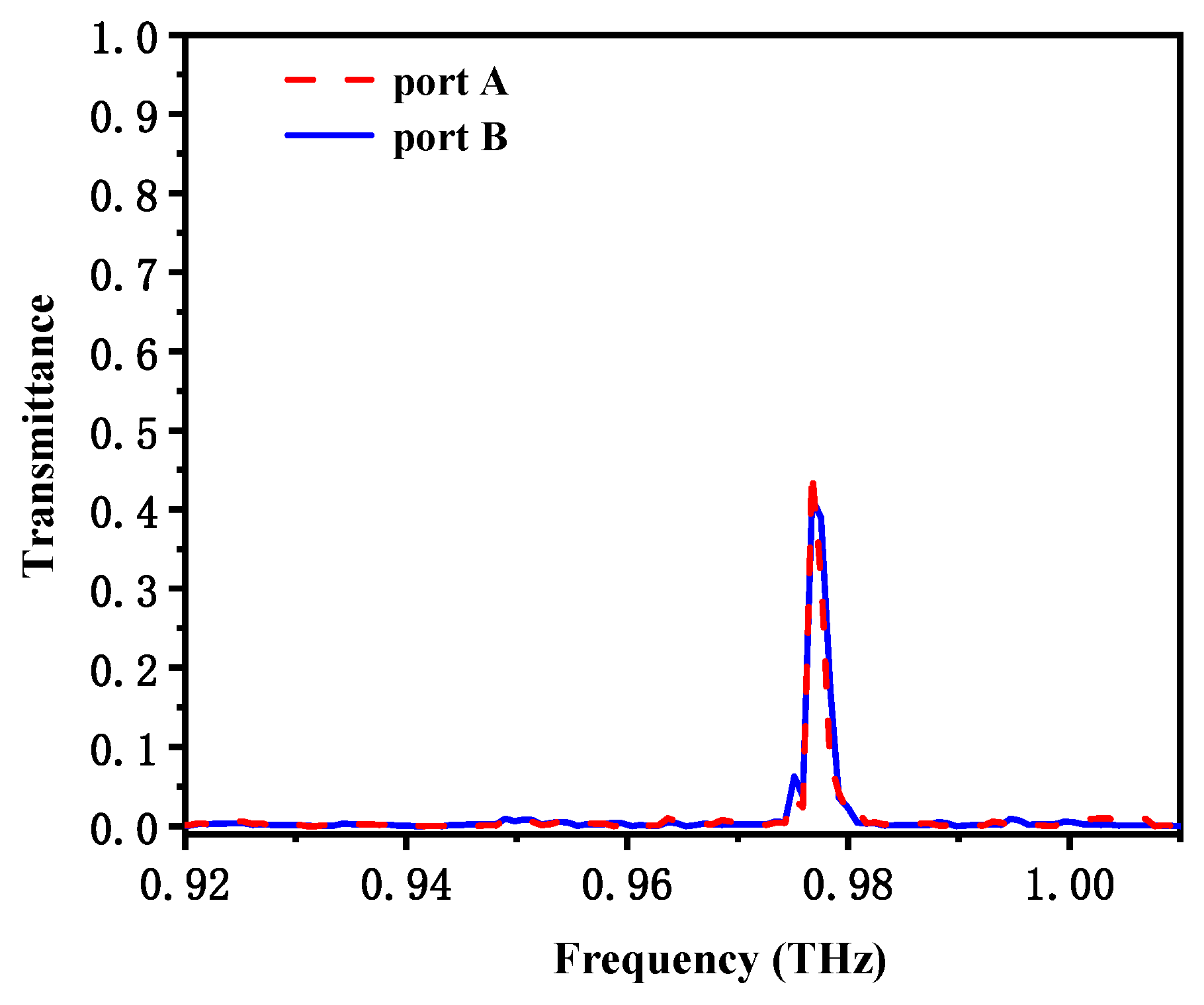
Next, we studied the transmission characteristics of the modulator in TM mode. Without pump excitation, the transmittance spectra of modulator from ports A and B in TM mode with frequencies of 0.92–1.01 THz is shown in Figure 4. It can be seen from Figure 4, only 0.977 THz of the center frequency produces weak resonance at the combined microcavity in the PBG range 0.92–1.01 THz and the transmittances of ports A and B are only 0.45 and 0.41, respectively. Therefore, we mainly discuss the TE mode with a larger PBG and higher resonance in the following.

3.2. Modulator Performance Analysis

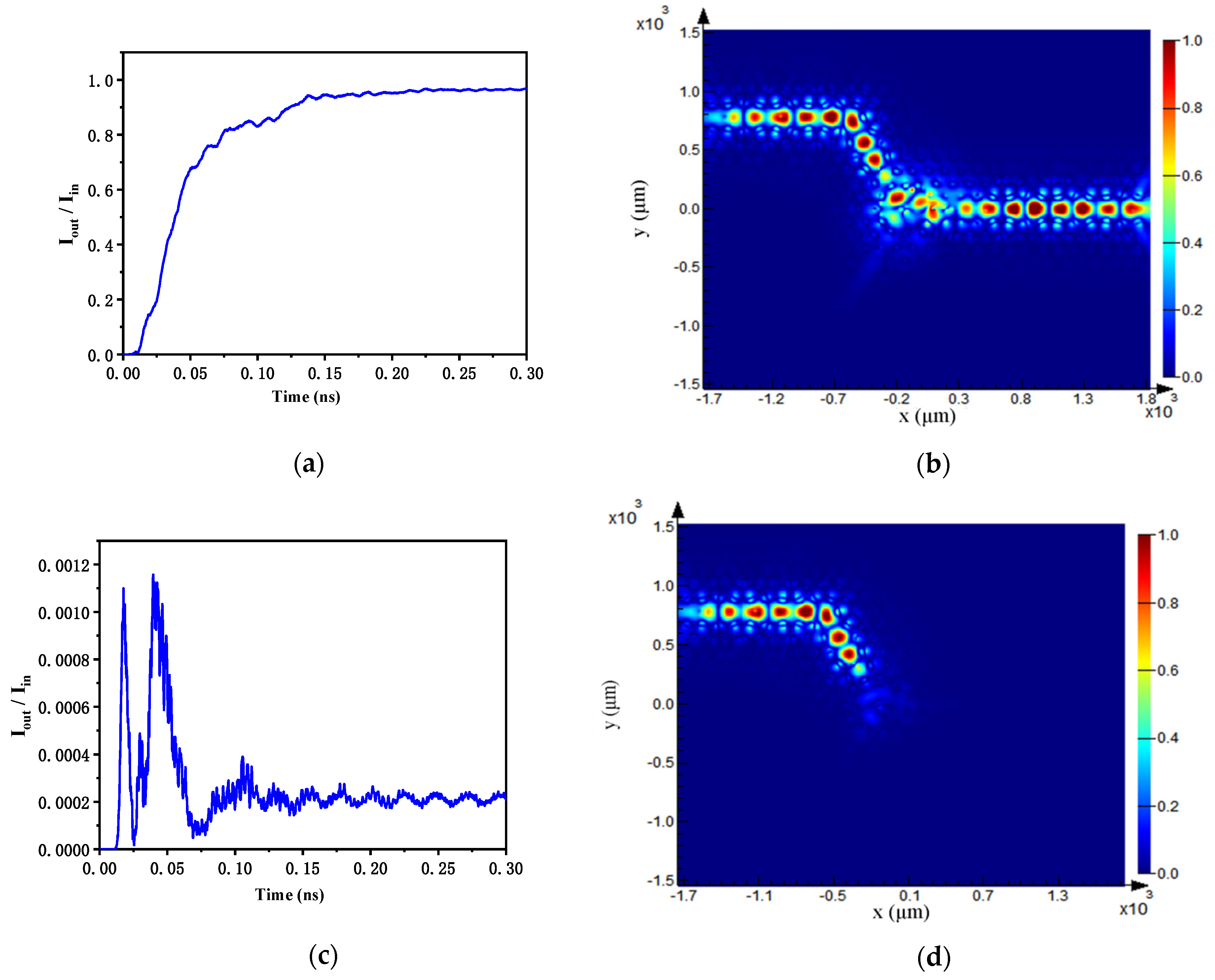
We first analyzed the case where ports A and C were used as the input and output ports, respectively. The single-frequency continuous-wave THz source is set at the input port of the modulator, and the monitor is placed at the output port. Without pump excitation, the corresponding steady-state THz wave field intensity distribution and time-domain steady-state response of the modulator are calculated by the FDTD method and visualized in Figure 5a,b, respectively. As shown in Figure 5a, the incident wave (f = 1.34 THz) is input from port A and output from port C with low transmission loss, and the ratio of output to input THz wave intensity is as high as 0.93. It is clearly seen from Figure 5b that the incident wave (f = 1.34 THz) can directly pass through the combined microcavity and be coupled to line defects for transmission. The modulator is in the ON state. With pump excitation, the refractive index of GaAs changes to 3.55 − i2.55 and the defect mode frequency at 1.34 THz disappears. The corresponding steady-state THz wave field intensity distribution and time-domain steady-state response are indicated in Figure 5c,d. As can be seen from Figure 5c, the ratio of output to input THz wave intensity (f = 1.34 THz) is only 0.0002. It can be observed from Figure 5d that the energy of the THz wave is concentrated in line defects in front of the point defect and cannot pass through the combined microcavity. There is almost no mode field energy distribution at the outlet end. The modulator is in the OFF state.
We calculated the insertion loss of the modulator when port A is the input port and port C is the output port. The insertion loss γ is defined by following equation [39]:
γ ( d B ) = 10 lg ( I i n / I o u t max ) ,
where I i n is the input intensity of the THz wave to the modulator, I o u t max is the maximum output intensity of the THz wave after modulation, and I o u t max / I i n is 0.93 according to Figure 5a. The insertion loss γ is calculated to be 0.31 dB, which is greatly reduced compared with the minimum insertion loss of 0.46 dB [24] reported in the current literature.
We also calculated the modulation depth (MD) of the modulator when port A is the input port and port C is the output port. The MD is defined as following [39]:
M D = ( I 1 I 0 / I 1 ) ,
where I1 is the output intensity of the THz wave in the ON state of the modulator and I0 is the output intensity of the THz wave in the OFF state. Since the intensity of the input THz wave remains invariant, according to Figure 5a,c, the modulation depth MD = (0.93 − 0.0002)/0.93 ≈ 100%, which is greatly improved compared with the maximum modulation depth of 94% reported in the current literature [40]. It is noteworthy that the modulation rate is related to not only the response time of nonlinear optical materials but also the steady-state response time of the system. The response time of the nonlinear optical-controlled material GaAs that is used in the simulation is about 100 ps [41]. It can be seen from Figure 5a that the steady-state response time when the system tends to be stable is about 0.15 ns, thus the maximum modulation rate is about 4.05 GHz (1/0.25 ns), which is greatly increased compared with the maximum modulation rate of 3 GHz reported in the current literature [42].
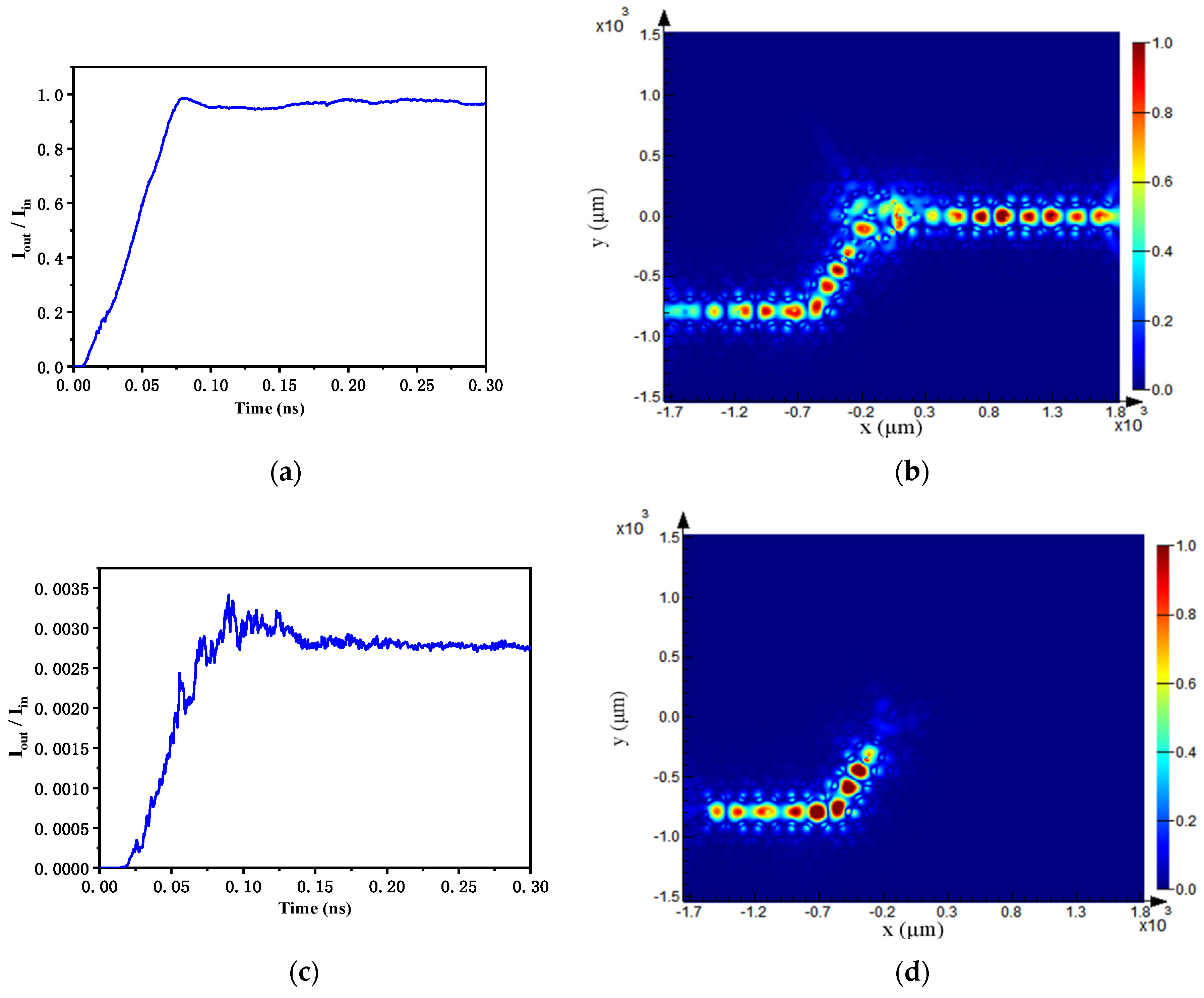
Next, we analyzed the case where ports B and C were used as the input and output ports, respectively. Without pump excitation, the corresponding steady-state THz wave field intensity distribution and time-domain steady-state response of the modulator are calculated by the FDTD method and presented in Figure 6a,b. It can be seen from Figure 6a,b that in the ON state without pump excitation, the incident wave (f = 1.83 THz) is input from port B and output from port C with low transmission loss, and the ratio of output to input THz wave intensity is as high as 0.96. In contrast, in the OFF state with pump excitation, Figure 6c,d illustrates the corresponding steady-state THz wave field intensity distribution and time-domain steady-state response. The incident wave (f = 1.83 THz) cannot pass through the combined microcavity. There is almost no mode field energy distribution at the outlet end, and the ratio of output to input THz wave intensity is only 0.0027. Accordingly, taking port B as the input, the insertion loss of the modulator is calculated to be 0.18 dB, and the modulation depth is as high as 99.7%. Additionally, the steady-state response time of the system is about 0.14 ns and the maximum modulation rate is about 4.17 GHz (1/0.24 ns). Compared with the performance parameters of the modulator when port A is used as the input, the modulation rate and insertion loss are further improved when port B is used as the input, and the modulation depth is also enhanced compared with the literature [40].
We compared the modulation depth, modulation rate, and insertion loss of the developed modulator to the parameters of similar THz devices developed. He et al. studied the effect of passivation on the fast carrier dynamics in GaAs and the modulation performance of a GaAs-based THz modulator by optically pumped terahertz probe technology. Under the appropriate excitation intensity, the maximum average modulation depth could reach 94%, and the modulation rate was 69 MHz [40]. Zhao et al. proposed a very high speed THz modulation mechanism based on tunable collective individual state conversion with a staggered netlike active two-dimensional electron gas metasurface. The modulation rate could reach 3 GHz, and the modulation depth could reach 93% [42]. Faramarz et al. Designed and optimized a high-speed and highly efficient THz intensity modulator with external power-dependent characteristics. The modulation rate could reach 3 GHz, the insertion loss was 2.2 dB, and the modulation depths were up to 99% [15]. The results, as shown in Table 2, indicate that the dual-channel modulator has good performance. It has high modulation depth (100%, 99.7%), fast modulation rate (4.05 GHz, 4.17 GHz), and good insertion loss (0.31 dB, 0.18 dB). The analysis shows that the high-performance THz wave modulator based on the combined microcavity can realize the ON–OFF regulation of optical signals and will play an essential role in becoming integrated into the optical path and THz wave communication, such as in optical add-drop multiplexers (OADMs) and real-time monitoring systems, etc.
This paper also studies the tolerance of errors that may occur in the production stage of the equipment. According to the radius shift of the silicon dielectric cylinder (the radius shift range is 32.52–33.69 μm), the modulation depth, modulation rate, and insertion loss of the modulator are obtained, as shown in Figure 7. In these three figures, when the radius of the silicon dielectric cylinder is 33.12–33.37 μm, 33.22–33.42 μm, and 33.19–33.42 μm, the modulation depth, modulation rate, and insertion loss remain unchanged. Based on the above analysis, it can be concluded that the silicon radius with 33.22–33.37 μm is the allowable error range for equipment processing.

4. Conclusions

We present a high-performance dual-channel photonic crystal THz wave modulator based on the defect mode disappearance of a combined microcavity that is designed and simulated by PWM and FDTD methods. The modulator is composed of silicon rod photonic crystals, introduced Y-type line defects as a dual-channel waveguide, and point defects and a ring resonator to form a combined microcavity. Due to the refractive index of the ring resonator filler, gallium arsenide, it is tunable with pump excitation; the defect mode frequency of the combined microcavity can be dynamically changed. Under pump excitation with a wavelength of 810 nm and an intensity of 0.4 μJ/cm2, 1.34 THz and 1.83 THz incident waves transmitted in the upper and lower channels are realized in the OFF state. The dual-channel modulator has modulation depths of 100% and 99.7%, modulation rates of 4.05 GHz and 4.17 GHz, and insertion losses of 0.31 dB and 0.18 dB, respectively. The results reveal that the modulator has virtues of high modulation depth, high modulation rate, low insertion loss, and low required pump power, which will play a crucial role in the prospective THz wave broadband wireless communication system.

Author Contributions

Conceptualization, G.L.; methodology, G.L., J.T. and Y.X.; software, J.T. and Y.X.; validation, G.L., J.T. and Y.X.; formal analysis, G.L., B.T. and N.X.; investigation, J.Z., W.Z. and N.X.; resources, B.T., H.C. and Z.J.; writing-original draft preparation, J.T. and Y.X.; writing—review and editing, G.L.; supervision, W.Z., H.C., Z.J. and N.X.; project administration, G.L. and J.Z.; funding acquisition, G.L. All authors have read and agreed to the published version of the manuscript.

Funding

This work was supported by the National Natural Science Foundation of China (Grant Nos. 62205194 and 52177185), Natural Science Foundation of Shanghai (Grant Nos. 17ZR1411500 and 20ZR1466300).

Institutional Review Board Statement

Not applicable.

Informed Consent Statement

Informed consent was obtained from all subjects involved in the study.

Data Availability Statement

Not applicable.

Conflicts of Interest

The authors declare no conflict of interest.

References

  1. Victor, P.P. Terahertz technologies and its applications. Electronics 2021, 10, 268. [Google Scholar]
  2. Ke, L.; Zhang, L. Corneal elastic property investigated by terahertz technology. Sci. Rep. 2022, 12, 19229. [Google Scholar] [CrossRef] [PubMed]
  3. Willner, A.E.; Su, X.Z. High capacity terahertz communication systems based on multiple orbital-angular-momentum beams. J. Opt.-UK 2022, 24, 124002. [Google Scholar] [CrossRef]
  4. Wei, M.; Zhang, D. High-performance all-optical terahertz modulator based on graphene/TiO2/Si trilayer heterojunctions. Nanoscale Res. Lett. 2019, 14, 1–6. [Google Scholar] [CrossRef] [PubMed]
  5. Ma, H.; Wang, Y. A flexible, multifunctional, active terahertz modulator with an ultra-low triggering threshold. J. Mater. Chem. C 2020, 8, 10213–10220. [Google Scholar] [CrossRef]
  6. Vitor, D.; Geraldo, M. Tunable THz switch-filter based on magneto-plasmonic graphene nanodisk. IEEE Trans. Magn. 2021, 57, 2900209. [Google Scholar]
  7. Liu, J.B.; Li, P.J. Flexible terahertz modulator based on coplanar-gate graphene field-effect transistor structure. Opt. Lett. 2016, 41, 816–819. [Google Scholar] [CrossRef]
  8. Huang, J.W.; Song, Z.Y. Terahertz graphene modulator based on hybrid plasmonic waveguide. Phys. Scr. 2021, 96, 1402–4896. [Google Scholar] [CrossRef]
  9. Huang, Y.D.; Yu, Y. Plasmonic terahertz modulator based on a grating-coupled two-dimensional electron system. Appl. Phys. Lett. 2016, 109, 201110. [Google Scholar] [CrossRef]
  10. Zhang, Y.X.; Qiao, S. Gbps terahertz external modulator based on a composite metamaterial with a double-channel heterostructure. Nano Lett. 2015, 15, 3501–3506. [Google Scholar] [CrossRef]
  11. Zheng, W.; Fan, F. Optically pumped terahertz wave modulation in MoS2-Si heterostructure metasurface. AIP Adv. 2016, 6, 075105. [Google Scholar] [CrossRef] [Green Version]
  12. Wang, H.X.; Ling, F.R. A terahertz wave all-optical modulator based on quartz-based MAPbI3 thin film. Opt. Mater. 2022, 127, 112235. [Google Scholar] [CrossRef]
  13. Kowerdziej, R.; Jaroszewicz, L. Active control of terahertz radiation using a metamaterial loaded with a nematic liquid crystal. Liq. Cryst. 2016, 43, 1120–1125. [Google Scholar] [CrossRef]
  14. Li, J.S. Terahertz modulator using photonic crystals. Opt. Commun. 2007, 269, 98–101. [Google Scholar] [CrossRef]
  15. Faramarz, A.; Zahra, H. Design and analysis of a high-performance terahertz photoconductive modulator enhanced by photonic crystal cavity. Appl. Phys. B-Lasers Opt. 2022, 128, 211. [Google Scholar]
  16. Chen, H.M.; Su, J. Optically-controlled high-speed terahertz wave modulator based on nonlinear photonic crystals. Opt. Express 2011, 19, 3599. [Google Scholar] [CrossRef]
  17. Moradi, M.; Mohammadi, M. Design and simulation of a fast all-optical modulator based on photonic crystal using ring resonators. Silicon 2022, 14, 765–771. [Google Scholar] [CrossRef]
  18. Wu, F.; Chen, M.Y. Omnidirectional terahertz photonic band gap broaden effect in one-dimensional photonic crystal containing few-layer graphene. Opt. Commun. 2021, 490, 126898. [Google Scholar]
  19. Wang, Y.L.; Chen, S.Y. Omnidirectional absorption properties of a terahertz one-dimensional ternary magnetized plasma photonic crystal based on a tunable structure. Results Phys. 2020, 18, 103298. [Google Scholar] [CrossRef]
  20. Osswa, S.; Sebastien, F. Tunable polychromatic filters based on semiconductor-superconductor-dielectric periodic and quasi-periodic hybrid photonic crystal. Opt. Mater. 2021, 111, 110690. [Google Scholar]
  21. Rakhshani, M.R.; Mansouri-Birjandi, M.A. Design and simulation of wavelength demultiplexer based on heterostructure photonic crystals ring resonators. Physica E 2013, 50, 97–101. [Google Scholar] [CrossRef]
  22. Mansouri-Birjandi, M.A.; Rakhshani, M.R. A new design of tunable four-port wavelength demultiplexer by photonic crystal ring resonators. Optik 2013, 124, 5923–5926. [Google Scholar] [CrossRef]
  23. Rakhshani, M.R.; Mansouri-Birjandi, M.A. Realization of tunable optical filter by photonic crystal ring resonators. Optik 2013, 124, 5377–5380. [Google Scholar] [CrossRef]
  24. Yan, D.X.; Li, J.S. Light-controlled tunable terahertz filters based on photoresponsive liquid crystals. Laser Phys. 2019, 29, 025401. [Google Scholar] [CrossRef]
  25. Gao, Y.F.; Wang, L.S. Transmission properties of one-dimensional magneto-optical photonic crystals containing graphene nanolayers. J. Supercond. Nov. Magn. 2019, 32, 1049–1055. [Google Scholar] [CrossRef]
  26. Jiang, Z.D.; Li, P.L. Light-control splitting ratio tunable Y-type Terahertz waves to beam splitter based on two-dimensional photonic crystal. J. Infrared Millim. W. 2020, 39, 561–566. [Google Scholar]
  27. Wang, Z.M.; Qiao, J. Recent progress in terahertz modulation using photonic structures based on two-dimensional materials. InfoMat. 2021, 3, 1110–1133. [Google Scholar] [CrossRef]
  28. Huang, Y.J.; Wang, Y. Tunable electro-optical modulator based on a photonic crystal fiber selectively filled with liquid crystal. J. Light. Technol. 2019, 37, 1903–1908. [Google Scholar] [CrossRef]
  29. Li, Z.J.; Kim, T.H. Wide-bandgap perovskite/gallium arsenide tandem solar cells. Adv. Energy Mater. 2020, 10, 1903085. [Google Scholar] [CrossRef]
  30. Mangla, O.; Savita, R. Synthesis of gallium arsenide nanostructures for solar cell applications. Mater. Lett. 2020, 274, 128036. [Google Scholar] [CrossRef]
  31. Yang, H.; Yun, G.H. Effects of point defect shapes on defect modes in two-dimensional magnonic crystals. J. Magn. Magn. Mater. 2014, 356, 32–36. [Google Scholar] [CrossRef]
  32. Ge, D.H.; Zhang, J.H.; Zhang, L.Q. Effect of Point and Linear Defects on Band-gap Properties in Triangular-Honeycomb Structure Photonic Crystals. In IOP Conference Series: Materials Science and Engineering; IOP Publishing Ltd.: Guangzhou, China, 2017; Volume 170, p. 012005. [Google Scholar]
  33. Kleine-Ostmann, T.; Koch, M. Modulation of THz radiation by semiconductor nanostructures. Microw. Opt. Technol. Lett. 2002, 35, 343–345. [Google Scholar] [CrossRef]
  34. Tiedje, H.F.; Haugen, H.K. Measurement of nonlinear absorption coefficients in GaAs, InP and Si by an optical pump THz probe technique. Opt. Commun. 2007, 274, 187–197. [Google Scholar] [CrossRef]
  35. Neamen, D.A. Semiconductor Physics and Devices, 2nd ed.; McGraw Hill Higher Education: New York, NY, USA, 2002. [Google Scholar]
  36. Fekete, L.; Kadlec, F. Ultrafast opto-terahertz photonic crystal modulator. Opt. Lett. 2007, 32, 680–682. [Google Scholar] [CrossRef]
  37. Javan, M.A.R.; Granpayeh, N. Fast terahertz wave switch/modulator based on photonic crystal structures. J. Electromagnet. Waves Appl. 2009, 23, 203–212. [Google Scholar] [CrossRef]
  38. Yablonovitch, A. Inhibited spontaneous emission in solid-state physics and electronics. Phy. Rev. Lett. 1987, 58, 2059–2062. [Google Scholar] [CrossRef] [PubMed] [Green Version]
  39. Lu, J.; Wang, D.; Chen, Y.F. Physics of Optoelectronic Devices, 2nd ed.; Publishing House of Electronics Industry: Beijing, China, 2009. [Google Scholar]
  40. He, Y.; Wang, Y. Enhanced performance of a fast GaAs-based terahertz modulator via surface passivation. Photonics Res. 2021, 9, 2230–2236. [Google Scholar] [CrossRef]
  41. Kuzel, P.; Kadlec, F. Propagation of terahertz pulses in photoexcited media: Analytical theory for layered systems. J. Chem. Phys. 2007, 127, 024506. [Google Scholar] [CrossRef]
  42. Zhao, Y.C.; Wang, L. High-speed efficient terahertz modulation based on tunable collective-individual state conversion within an active 3 nm two-dimensional electron Gas metasurface. Nano Lett. 2019, 19, 7588–7597. [Google Scholar] [CrossRef]
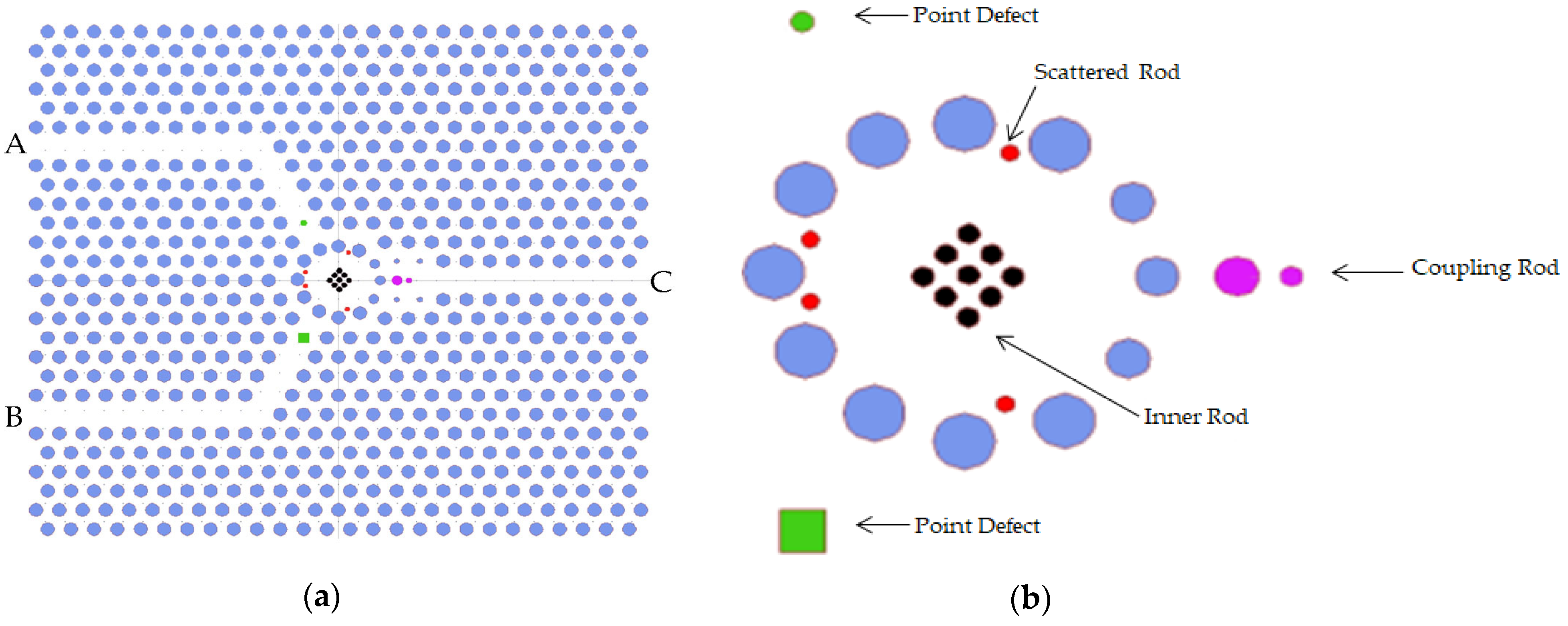
Figure 1. (a) The structure model of 2D photonic crystal THz wave modulator. (b) Sectional view of combined microcavity.
Photonics 10 00298 g001
Figure 2. TE (blue) and TM (red) modes of energy band diagram for perfect photonic crystal.
Photonics 10 00298 g002
Figure 3. (a) Transmittance spectrum of modulator from input port A in TE mode with (dashed line) and without pump excitation (solid line). (b) Transmittance spectrum of modulator from input port B in TE mode with (dashed line) and without pump excitation (solid line).
Photonics 10 00298 g003
Figure 4. Transmittance spectrum of the modulator from ports A and B in TM mode without pump excitation.
Photonics 10 00298 g004
Figure 5. Port A as the input port. The time domain steady-state response (a) and steady-state field distribution (b) without pump excitation, and the time domain steady-state response (c) and steady-state field distribution (d) with pump excitation.
Photonics 10 00298 g005
Figure 6. Port B as the input port. The time domain steady-state response (a) and steady-state field distribution (b) without pump excitation, and the time domain steady-state response (c) and steady-state field distribution (d) with pump excitation.
Photonics 10 00298 g006
Figure 7. (a) The modulation depth of input port A and port B with the radius of the silicon dielectric cylinder in the range of 32.52–33.69 μm. (b) The modulation rate of input port A and port B with the radius of the silicon dielectric cylinder in the range of 32.52–33.69 μm. (c) The insertion loss of input port A and port B with the radius of the silicon dielectric cylinder changes in the range of 32.52–33.69 μm.
Photonics 10 00298 g007
Table 1. Structure model parameters of photonic crystal THz modulator.
NameSymbolAttribute
The lattice constanta119 μm
The radius of circular silicon rodsR0.28a
The refractive index of siliconn3.4
The circular rod (green color)r0.1a
The square rod (green color)l0.42a
The inner rods (black color)b0.1a
The scattered rods (red color)s0.08a
The coupling rods (purple color)p0.2a
Table 2. Performance comparison.
ModulationInput PortTransmissivity (%)Modulation Depth (%)Modulation Rate (GHz)Insertion Loss (dB)
[24]No input portNot providedNot providedNot provided0.46
[40]One input portNot provided940.069Not provided
[42]One input portNot provided933Not provided
[15]One input portNot provided9932.2
dual-channel modulatorAON931004.050.31
OFF0.02
BON9699.74.170.18
OFF0.27
Disclaimer/Publisher’s Note: The statements, opinions and data contained in all publications are solely those of the individual author(s) and contributor(s) and not of MDPI and/or the editor(s). MDPI and/or the editor(s) disclaim responsibility for any injury to people or property resulting from any ideas, methods, instructions or products referred to in the content.