1. Introduction
Phase shifting plays an important role in a radar system. The pulse compression signal based on the phase-coded microwave signal solves the contradiction between the detection range and the range resolution in the radar system by expanding the signal bandwidth of the transmitted signal and realizing the pulse compression at the receiving end through the matched filter. However, the traditional electronic microwave phase shifter has a limited phase shift range and working bandwidth. Therefore, a microwave photonic phase shifter has been proposed to generate a high-frequency, broadband, and tunable phase-coded microwave signal by controlling the phase of the microwave signal in the optical domain [
1,
2], revealing important application prospects [
3,
4,
5].
To date, many schemes have been proposed to realize microwave photonic phase shifting, including phase shifting based on heterodyne mixing technology, which can be divided into integrated parallel modulator structures and series modulator structures. First, in the scheme involving the realization of 360° continuous phase tuning by adjusting the direct current (DC) bias voltage of the integrated parallel modulator, the radio frequency (RF) signal modulation and phase shifting are completed with the same equipment. However, this is not applicable to the array phase-shifting application, which requires multiple independent phase adjustments; in addition, the modulation bandwidth of the bias port limits its high-speed phase-coded applications [
6,
7,
8]. The series modulator structure, based on polarization adjustment, realizes the phase shifting mainly by inputting the polarization orthogonal signals obtained by RF signal modulation into the polarization-related devices, such as the phase modulator (PM), the polarization modulator (PolM), or the polarization controller (PC). By adjusting the DC driving voltage [
9,
10,
11] of the PM or the PolM, or by mechanically adjusting the PC [
12,
13], the two polarization orthogonal signals are introduced into different optical phase shifts, and finally, the microwave signals with continuous phase changes are obtained by the photodetector.
The optical heterodyne method can be used to generate phase-coded microwave signals when using a multilevel control voltage to achieve specific phase adjustments. The parallel structure inputs the microwave signal and the coding signal into the two arms of a single integrated modulator at the same time; the modulator is used to load the frequency and the phase signal into the optical domain. Finally, the optical sideband signal with the frequency-modulated and phase-modulated optical carriers is input into the photodetector to beat the frequency, and the phase-coded signal is obtained [
14,
15,
16,
17]. In [
15], by accurately changing the bias voltage of the modulator and the input power of the local oscillator (LO) signal, binary phase-coded signals with different frequency multiplication factors were obtained. However, due to the better Doppler tolerance of multiphase coded signals, some studies have obtained binary or quaternary phase-coded signals by changing the waveform of the input coding signals, but the function of the carrier frequency reconfiguration was sacrificed [
16,
17].
This problem can be solved by adopting the serial structure, which inputs the microwave signal and the coding signal into two different modulators; this has the advantage of the independent modulation of the frequency and the phase and can allow the system to have multiple functions at the same time. In [
18], by adjusting the bias voltage of the dual-parallel dual-polarization Mach–Zehnder modulator (DP-DPMZM), the switching of the first-order or second-order sideband signals of the carrier suppression was realized. Then, the sidebands and carrier signals with orthogonal polarization were input into the PM for phase modulation, and the binary phase-coded signal of the fundamental or harmonic carrier frequency was obtained. In [
19], the DP-DPMZM was used to generate two single sideband signals with orthogonal polarization, which were input into a PolM driven by a three-level electrical coding signal to realize the phase coding, and finally, a doubled frequency phase-coded microwave pulse was generated through photoelectric conversion. However, both methods are based on the odd function characteristic of the sine function. Binary coding is realized by using the input coding signal with opposite polarity; therefore, the multiphase coded signals cannot be generated by using multilevel electrical coding signals.
In [
20,
21,
22,
23,
24,
25,
26,
27,
28,
29], the phase-coded signal was realized based on the amplitude modulation of the input coding signal; this has two advantages: one is that the phase can be adjusted by changing the amplitude of the input coding signal, and the other is that the multiphase coded signal can be obtained by using the stepped wave coding signal. In [
20,
21,
22], a fiber Bragg grating (FBG) was used to separate optical sidebands modulated by RF signals. With this method, one sideband was modulated by a PM driven by coding signals; the other sideband kept its initial phase, and the last two sidebands were simultaneously coupled to a photodetector (PD) to obtain phase-coded signals. Another method is to directly divide the optical carrier into two parts, which are modulated by the RF signal and the coding signal [
23] and finally coupled to a PD for photoelectric conversion. It is also common to generate phase-coded signals based on a polarization adjustment. The orthogonally polarized signals modulated by the RF signal are input into the PolM [
24,
25,
26] or PM [
27] driven by the coding signal to realize phase modulation; finally, an arbitrary phase-coded signal is obtained when the amplitude of the input coding signal is changed. In addition, in [
28], an arbitrary phase was also realized by applying multilevel voltage amplitudes, and the frequency multiplication factors of the phase-coded signals could be changed by changing the input phase of the RF signal and the bias configuration of the front-end modulator. However, an FBG was needed to filter the optical carrier when obtaining the carrier-suppressed single-sideband (CS-SSB) signal, and an additional thermostat was used to avoid the wavelength drift of the FBG. In [
29], the frequency multiplication factor was changed by accurately changing the bias voltage of the modulator and the phase of the electric phase shifter. However, the bandwidth and stability of the electric phase shifter may affect the performance of the system.
In this paper, a scheme for generating fundamental/doubled frequency phase-coded microwave signals based on polarization multiplexed technology is proposed. The +1st-order CS-SSB of the LO signal can be obtained in the X polarization state. By controlling the RF switch and the bias voltage of the modulator, the configuration of the Y-DPMZM can be changed, and the optical carrier or the −1st-order CS-SSB of the LO signal can be obtained, and then the reconfiguration of the carrier frequency can be realized. After the DP-DPMZM, the polarized orthogonal optical signal is input into the polarization-dependent phase modulator (PD-PM) to realize the phase modulation. The phase difference between the two polarized optical signals is proportional to the phase-modulated driving signal voltage. The coding signals with multilevel voltage are used for phase modulation, and an arbitrary phase-coded microwave signal can be obtained after the PD. The proposed scheme can guarantee the loading of the microwave carrier frequency and the phase coding independently; this can then be effectively applied to the generation of a multichannel phase-coded microwave signal with a common carrier frequency. The proposed scheme is experimentally evaluated.
2. Principle and Methods
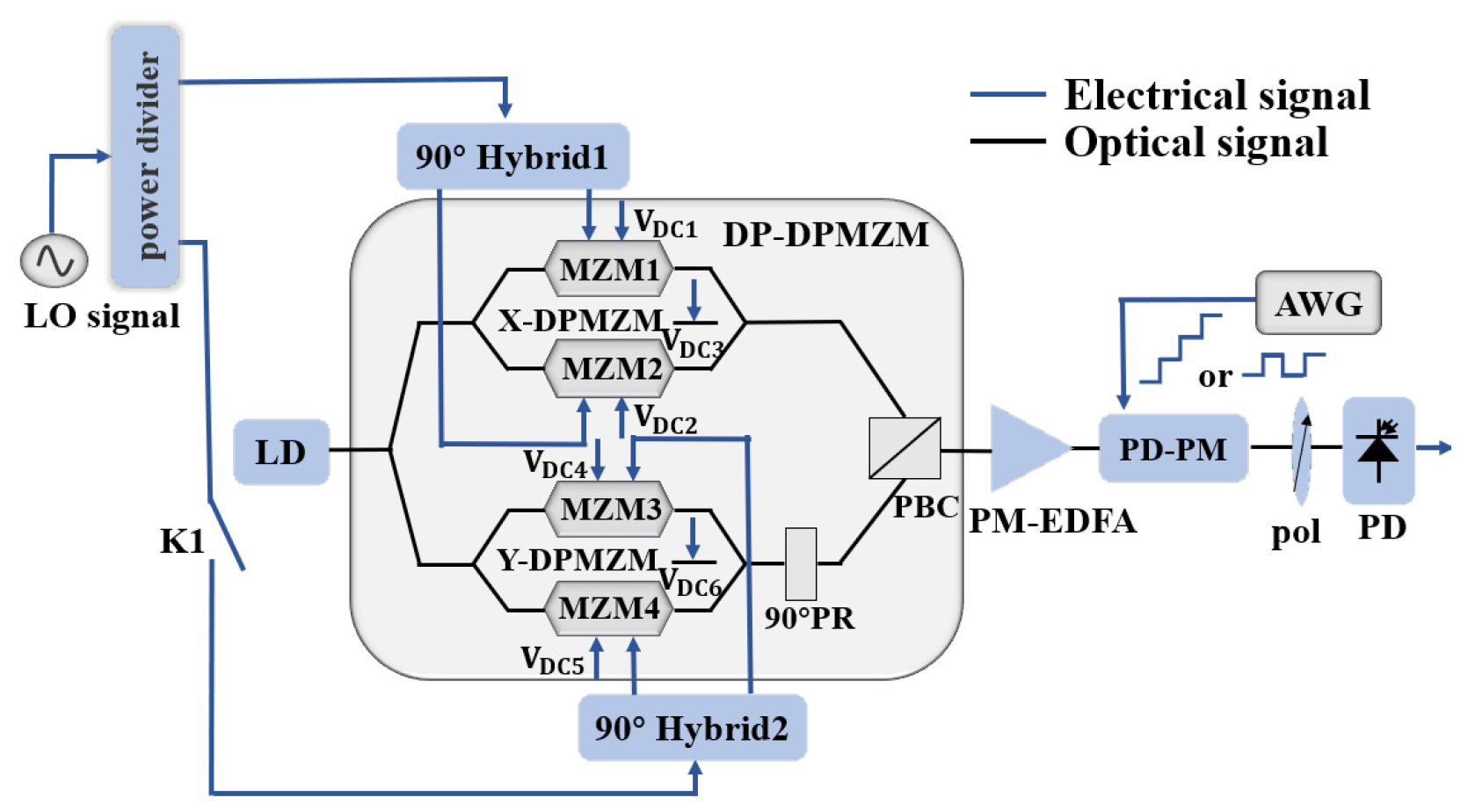
Figure 1 shows a schematic of the generation of a fundamental/doubled frequency phase-coded microwave signal based on polarization multiplexing technology. It contains a laser diode (LD), a radio frequency (RF) switch, a DP-DPMZM, two 90° hybrid couplers (HC), a PD-PM, a polarizer (Pol), a polarization-maintaining erbium-doped optical amplifier (PM-EDFA), and a photodetector (PD). The DP-DPMZM is composed of two sub-DPMZMs (an X-DPMZM and a Y-DPMZM) in parallel arms with a 90° polarization rotator (PR) after the Y-DPMZM. A polarization beam combiner (PBC) combines the output of the two sub-DPMZMs. Each sub-DPMZM consists of two sub-MZMs and three DC bias voltages, which are named sub-MZMn (
n = 1, 2…4) and
(i = 1, 2…6), respectively.
A continuous light wave produced by the LD is injected into the DP-DPMZM. The LO signal is divided into two parts through a power divider, one of which is input into the X-DPMZM through a 90° HC. When the DC bias voltage of the X-DPMZM is reasonably set, the +1st-order CS-SSB modulation of the LO signal in the X-DPMZM can be obtained. The other part is controlled by an RF switch. When the RF switch is in the open mode, the Y-DPMZM only outputs the optical carrier with a DC bias setting in the Y polarization state. When the RF switch is in the closed mode, the LO signal is input into the Y-DPMZM through a 90° HC. By reasonably setting the DC bias voltage of the Y-DPMZM, the −1st-order CS-SSB of the LO signal in the Y polarization state can be practically obtained. Then, the polarization multiplexed signal is input into the PD-PM, which is driven by the phase modulation voltage. The phase of a microwave signal can be tuned continuously by a phase modulation signal, and the carrier frequency is equal to or twice that of the LO signal. The arbitrary phase-coded signal is obtained when the RF port of the PD-PM is driven by a multilevel voltage signal.
The optical carrier from the LD is given by
, where
and
represent the angular frequency and amplitude of the optical carrier, respectively. The LO signal is divided into two parts by a power divider, one part of which is input into the X-DPMZM after passing through a 90° HC. In detail, the signal is first applied to the 90° HC; one path is sent to sub-MZM1, and the other path, with a 90° phase shift, is sent to sub-MZM2. The optical signal at the output of the X-DPMZM is
where
and
are the angular frequency and the amplitude of the LO signal;
is the modulation index of the sub-MZM;
corresponds to the phase shifts of the sub-MZM induced by the DC bias; and
is the half-wave voltage of the DP-DPMZM. In the small-signal modulation approximation, the high-order modulations (n ≥ 2) are neglected. Then, Equation (1) can be written as
where
is the
nth-order Bessel function of the first kind.
As seen in Equation (2), by biasing the two sub-MZMs at the minimum transmission point and the main MZM at the quadrature transmission point, which means that
and
, the +1st-order CS-SSB of the LO signal can be obtained, which can be given by
2.1. Generation of Arbitrary Phase Microwave Signal with a Fundamental Frequency
The other part of the LO signal is controlled by the RF switch to obtain the fundamental or doubled frequency modes. When the RF switch is in the open state, the Y-DPMZM is only biased with DC voltage. Setting
, the output of the Y-DPMZM is given by
Therefore, the optical field of the DP-DPMZM can be expressed as
The polarization-multiplexed optical signal is input into a PD-PM. A polarization-dependent phase modulator has different modulation efficiencies for TE and TM polarization. Therefore, the output expression of the PD-PM can be expressed as
where
and
are the phase shifts introduced by the PD-PM in the X and Y polarization states, respectively. A Pol is used to project the orthogonally polarized optical signal to the same polarization state as before the PD, and the output of the Pol can be given by
Suppose that the responsivity of the PD is
. Ignoring the DC component, the beating photocurrent can be expressed as
For the polarization-dependent phase modulator, the modulation efficiency in the TM polarization is approximately 3 times that in the TE polarization; and the optical phase difference is linearly related to the voltage of the PD-PM and can be expressed as
where
is the half-wave voltage of the PD-PM for the TM polarization;
is the phase-modulated voltage. Then, Equation (8) can be written as
Equation (10) shows that a microwave signal with a frequency equal to the LO signal is obtained and that the phase can be continuously adjusted by changing the driving voltage of the PD-PM.
2.2. Generation of an Arbitrary Phase Microwave Signal with a Doubled Frequency
When the RF switch is in a closed state, the Y-DPMZM is driven by the LO signal through a 90° HC. By setting
and
, the −1st-order CS-SSB of the LO signal can be obtained, and the output of the DP-DPMZM can be written as
Similarly, the PD-PM is driven by the phase-modulated voltage, and after photoelectric conversion, the output signal can be expressed as
By changing the configuration of the Y-DPMZM and the RF switch, the microwave signal has a frequency twice that of the LO signal.
2.3. Generation of Fundamental/Doubled Frequency Arbitrary Phase-Coded Signal
According to Equations (5) and (11), the orthogonally polarized optical signal in the fundamental or doubled frequency mode is obtained at the output of the DP-DPMZM, and the phase-coded signal can be realized by inputting it into the PD-PM driven by the coding signal.
Assuming that the PD-PM is driven by the coding signal
,
is the amplitude, and
is the coding mode. Hence,
Therefore, the PD output expression in the fundamental and doubled frequency modes can be written as
Overall, the Y-DPMZM configuration, which directly outputs the optical carrier or is set as the CS-SSB modulation of the LO signal, determines the generation of a fundamental or doubled carrier frequency, and the phase of the signal can be continuously changed by adjusting the driving voltage of the PD-PM. When the PD-PM is driven by a phase-coded signal, a fundamental or doubled frequency phase modulation coded signal can be obtained. The binary phase-coded signals are obtained by using square waves with the coding modes of ‘0’ and ‘1’. The multiphase coded signals can be realized by using the multilevel voltage. In other words, by adjusting the amplitude of the phase modulation coding signal, a microwave signal with any phase can be obtained.
3. Results
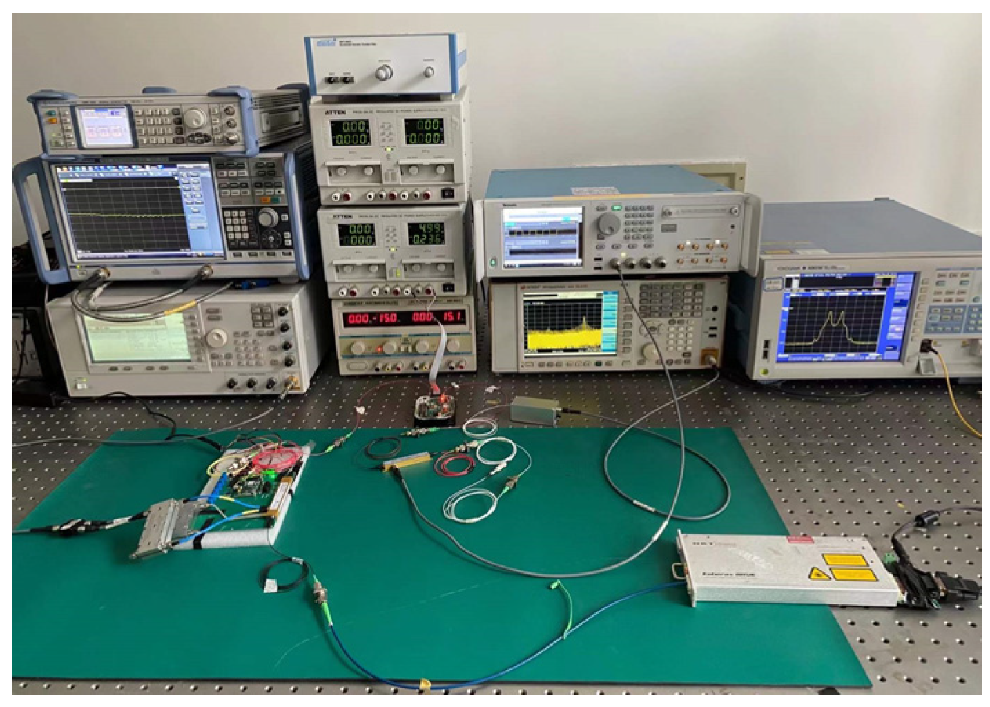
The experimental link was built according to the schematic diagram shown in
Figure 2. An LD (NKT, Koheras BASIK X15, Beijing, China) was used to generate the optical carrier with a wavelength of 1550.21 nm and a power of 15.5 dBm; the optical carrier was sent to a DP-DPMZM (Fujitsu, FTM7977HQA, Beijing, China) with a half-wave voltage of 3.5 V. The LO signal was generated by the microwave signal generator (MSG, Agilent, E8257D, Beijing, China) and sent to a DP-DPMZM through an electrical 90° hybrid coupler (Marki Microwave QH-0226, 2–26.5 GHz). The phase modulation signal that drives the PD-PM was generated from an arbitrary waveform generator (AWG, Tektronix AWG70002B, Beijing, China). A PD (Conquer, KG-PD-20G, 20 GHz, 0.75 A/W, Beijing, China) was used to realize the photoelectric conversion. In the experiment, a PM-EDFA was utilized to amplify the optical signals after the DP-DPMZM, and it functioned in an automatic power output control mode to ensure adequate signal power for the photoelectric detection. An optical spectrum analyzer (OSA, Yokogawa, AQ6370C, Beijing, China) and an oscilloscope (Tektronix DPO75902SX, Beijing, China) were employed to monitor the optical spectra and waveforms, respectively.
3.1. Generation of a Reconfigurable Carrier Frequency Microwave Signal with Phase-Shifting Capability
The performance of the reconfigurable carrier frequency and the phase shifting was demonstrated. The LO signal, with a frequency of 8 GHz and a power of 15 dBm, was input into the power divider and divided into two parts, one of which was input into the X-DPMZM through a 90° HC; in addition, the DC bias voltage of the X-DPMZM satisfied
and
to realize the +1st-order CS-SSB modulation of the LO signal. The other part was controlled by an RF switch. To obtain the fundamental carrier frequency signal, the RF switch was opened, and the bias voltage of the Y-DPMZM was adjusted to make
. Then, the Y-DPMZM only output an optical carrier. As the output of the DP-DPMZM combines the output of the X- and the Y-DPMZM through a PBC, the output optical signal of the DP-DPMZM is in an orthogonal polarization state, and both outputs can be distinguished by polarization control (PC) combined with a Pol.
Figure 3a shows the output spectra of the X-DPMZM, Y-DPMZM, and DP-DPMZM in the fundamental frequency mode. The carrier and −1st-order sideband suppression ratios in the X polarization state are 23.5 dB and 32.8 dB, respectively. Only the optical carrier is contained in the Y polarization state.
Figure 3b shows the output spectra of the X-DPMZM, Y-DPMZM, and DP-DPMZM in the doubled frequency mode. The configuration of the X branch is kept unchanged, and the RF switch is closed. The bias voltage of the Y-DPMZM is adjusted to satisfy
and
. The carrier and +1st-order sideband suppression ratios in the Y polarization state are 22.6 dB and 36.7 dB, respectively.
Next, a vector network analyzer was used to verify the broadband operation ability of the proposed scheme in the fundamental carrier frequency mode. First, as shown in
Figure 4a, a continuous 360° phase shift with a frequency bandwidth of 3–18 GHz was realized by adjusting the phase modulation driving voltage of the PD-PM. The frequency modulation range was limited by the bandwidth of the photodetector. The phase deviation was measured as be ±2.5°, and the voltage difference was approximately 8 V in a phase shift range of 360°. Then, the power response of the signal at different phase shifts was tested, as shown in
Figure 4b, and the maximum variation range was ±1.25 dB.
Figure 4c,d illustrates the stability of the system by testing the phase drift and power ripple with a phase shift of 90° within 5 min. The results show that the phase drift was less than 3°, and the power change was less than 1.23 dB. An oscilloscope (Agilent 86100C) was used to verify the phase-shifting ability of the doubled frequency microwave signal generated when the LO signal was 8 GHz. As shown in
Figure 4e, the waveforms of the doubled frequency microwave signal with phases of 0°, 90°, 180°, 270°, and 360° were obtained. Then, the LO signal was set to change at 2–9 GHz with a step of 1 GHz, and the power change in the doubled frequency microwave signal was observed with a spectrometer; its value was within 3 dB, as shown in
Figure 4f. Finally, the LO signal was fixed at 8 GHz, and the stability of the power of the generated doubled frequency microwave signal within 5 min was tested, as shown in
Figure 4g, and it was determined to be almost unchanged.
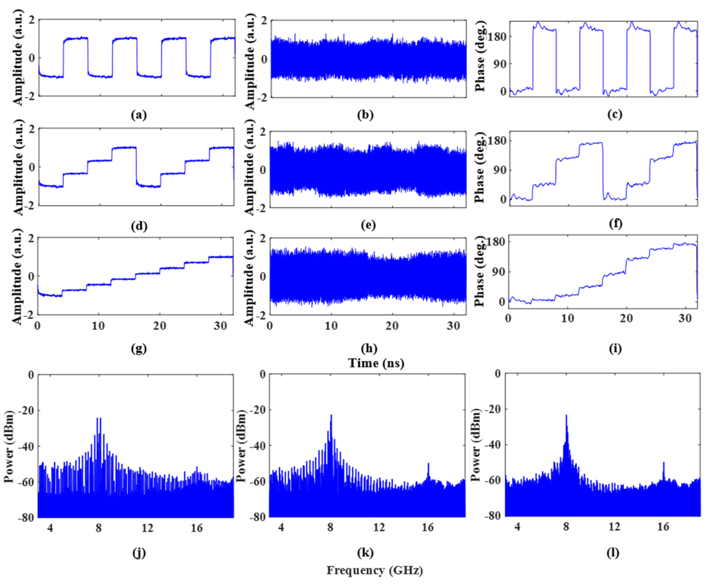
When the RF port of the PD-PM is driven by coding signals, the performance of the system in realizing the arbitrary phase-coded microwave signals is verified. An AWG was used to generate 2-, 4-, and 8-level voltage coding signals with a symbol rate of 250 Mb/s; these were amplified by an electric amplifier and then input into the RF port of the PD-PM. Then, the binary, quaternary, and octonary phase-coded signals could be obtained.
Figure 5 and
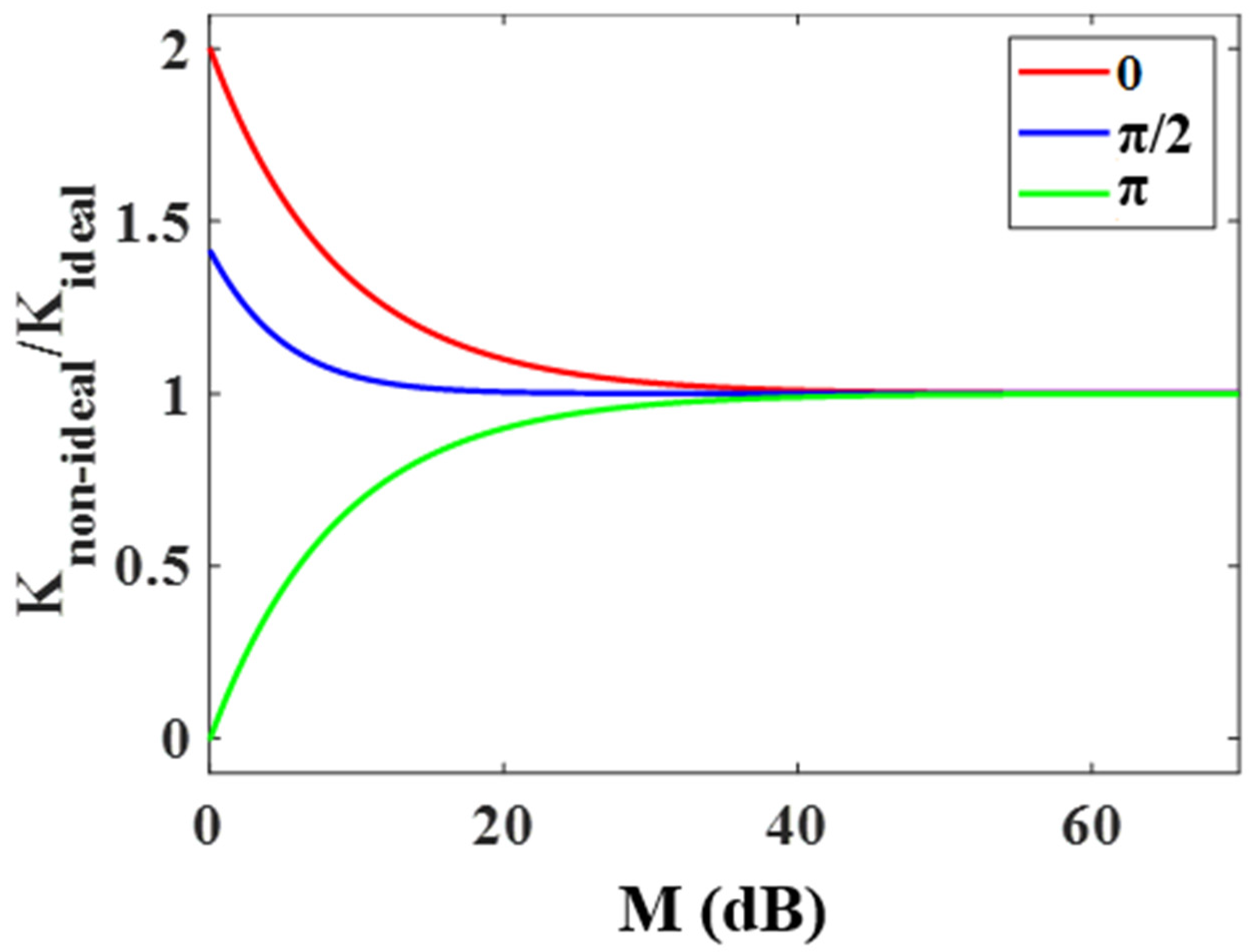
Figure 6 show the waveform of the original coding signal, the waveform diagrams of the fundamental and doubled frequency phase-coded signals with carrier frequencies of 8 GHz and 16 GHz, and the corresponding phase information and frequency spectrum, respectively. It can be seen that the system has realized the arbitrary phase-coded signals. However, due to the limited extinction ratio of the commercial modulators, the optical carrier and the unwanted sideband of the LO signal cannot be completely suppressed. Therefore, even if the modulator is accurately biased at the corresponding transmission point, there will still be some residual optical carriers and unwanted sidebands after the output of the modulator, which will cause some redundant unchanged phase signals after the photoelectric conversion. With the vector synthesis of the same frequency of phase-coded and redundant phase invariant signals, the amplitude of the output signal will change. A simulation was established to analyze the change in the amplitude ratio relative to the carrier suppression ratio in the nonideal (i.e., with residual optical carriers) and the ideal suppression under different phase shifts. The results are shown in
Figure 7. With the increase in the carrier suppression ratio
M, the ratio gradually approaches 1, which is the ideal state. When
, different signals have different amplitude fluctuations, but the whole is within 11.5%. If the optical carrier and the sideband of the LO signal in the experiment are suppressed as much as possible, the above phenomenon will be satisfactorily solved.
3.2. Generation of Binary Phase-Coded Microwave Signal with Reconfigurable Carrier Frequency
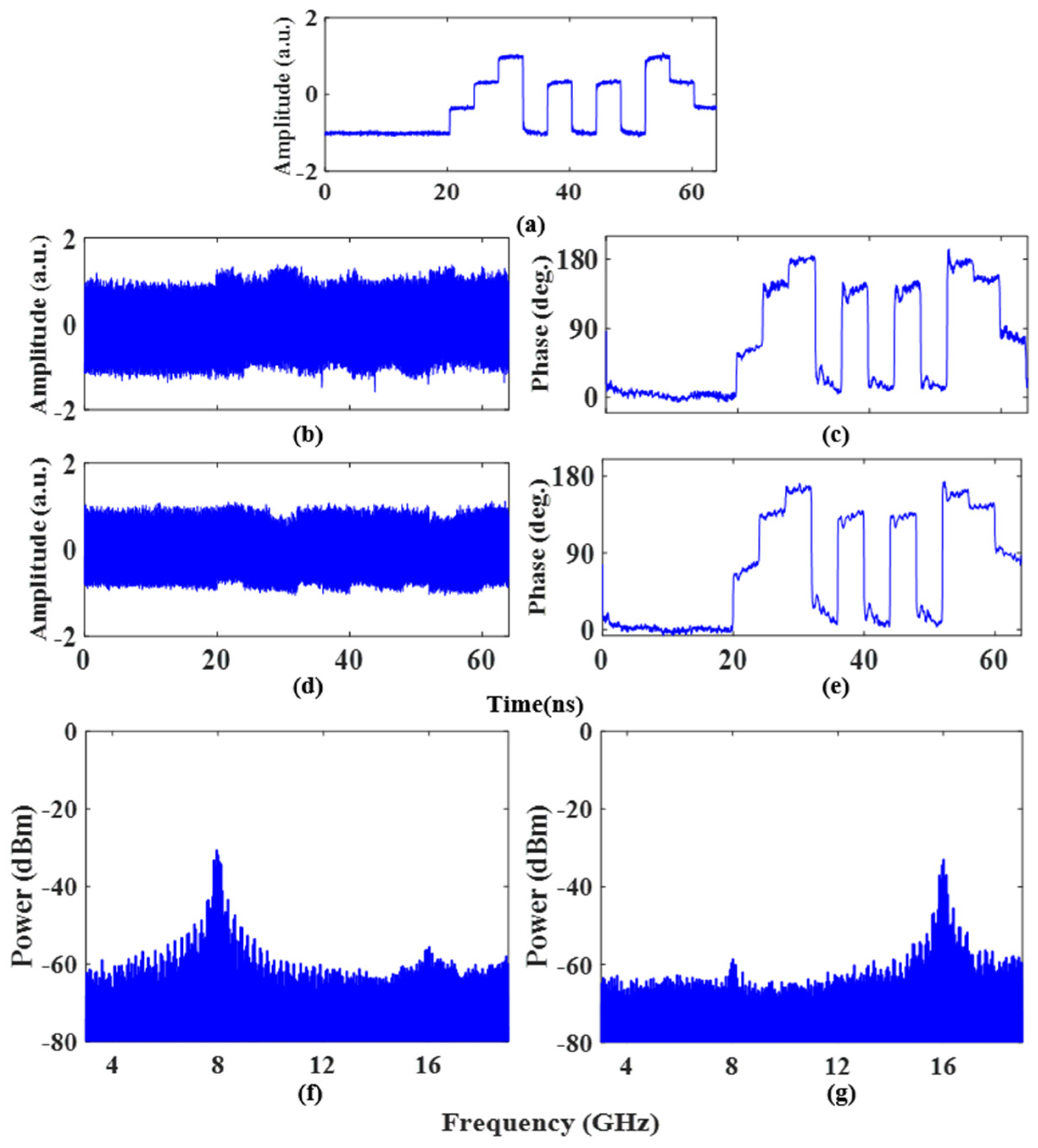
The radar receiver operates the cross-correlation between the microwave pulse and its echo to obtain a relatively narrow pulse. Therefore, calculating the autocorrelation performance is a common method used in evaluating the pulse compression capability of microwave signals. To verify the phase recovery accuracy and the pulse compression. Performance of the binary phase-coded signal generated by the proposed system, the PD-PM was driven by a 2-level phase-coded voltage with a coding rate of 250 Mb/s, and the coding mode was “1,1,1,1,1,0,0,1,1,0,1,0,1”, the waveform of the original coding signal as shown in
Figure 8a.
Figure 8b,c show the waveforms of the binary phase-coded signals in the fundamental carrier frequency mode and its extracted phase information when the frequency of the LO signal is 8 GHz, respectively.
Figure 8d,e shows the waveforms of the binary phase-coded signal in the doubled carrier frequency mode and its extracted phase information, respectively. The corresponding spectrum diagram is shown in
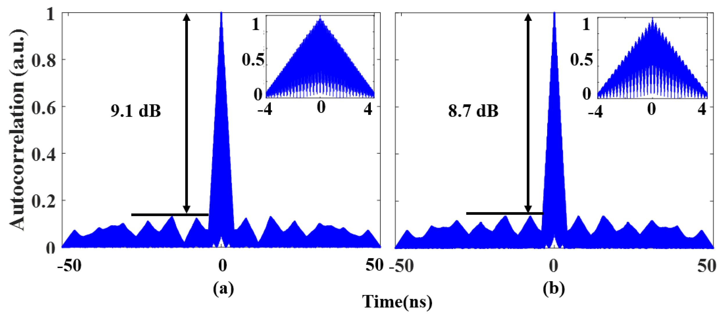
Figure 8f,g. To evaluate the pulse compression capability of the proposed system, the autocorrelations of the phase-coded signals were calculated, and the results are shown in
Figure 9.
Figure 9a shows the autocorrelation results in the fundamental carrier frequency mode. The peak-to-sidelobe ratio (PSR) is defined as the ratio of the peak power of the main lobe to that of the highest sidelobe; in this case, it was 9.1 dB. The more sidelobe suppression there is, the lower the interference. The full width at half maximum (FWHM) was 4.0 ns. The pulse compression ratio (PCR) is defined as the ratio of the pulse width before compression to the signal FWHM after compression; this was calculated as 13, and its theoretical value was equal to the symbol sequence length. The autocorrelation result in the doubled carrier frequency mode is shown in
Figure 9b, where the PSR, FWHM, and PCR are 8.7 dB, 4.1 ns, and 12.7, respectively.
3.3. Generation of Quaternary Phase-Coded Microwave Signal with Reconfigurable Carrier Frequency
Similarly, a 4-level coding signal was input into the RF port of the PD-PM to generate a quaternary phase-coded signal with a reconfigurable carrier frequency. The sequence pattern was set as “0,0,0,0,0,1,2,3,0,2,0,2,0,3,2,1”, with the waveform of the original coding signal, as shown in
Figure 10a.
Figure 10b,d shows the waveforms of the fundamental and doubled carrier frequency quaternary phase-coded signals, respectively. The corresponding recovered phase information is shown in
Figure 10c,e, and the 4-level phase jumps can be observed in the experimental results. The corresponding spectrum diagram is shown in
Figure 10f,g. The corresponding pulse compression performance is shown in
Figure 11. In the fundamental carrier frequency mode, the PSR, FWHM, and PCR are 4.8 dB, 4.5 ns, and 14.2, respectively, as shown in
Figure 11a. In the doubled carrier frequency mode, as shown in
Figure 11b, the PSR, FWHM, and PCR are 4.1 dB, 5 ns, and 12.8, respectively. It should be noted that a higher PCR will be obtained if a longer symbol sequence is used. A higher PCR means a larger time–bandwidth product (TBWP), which can increase the resolution of the radar systems.
The cascade phase-coded signal generator proposed in this paper can guarantee the loading of the microwave carrier frequency and the phase coding independently; this can then be effectively applied to the generation of a multichannel phase-coded microwave signal with a common carrier frequency. In the fundamental carrier frequency mode, the operating frequency range of the proposed scheme is only limited by the operating bandwidth of the frequency-dependent devices, such as the 90° hybrid, the DP-QPSK modulator, and the PD. In the doubled carrier frequency mode, the 90° hybrid DP-QPSK modulator needs only half the bandwidth of the system. The bandwidth of the system is mainly limited by the PD, while the commercially available 90° hybrid is already able to work in the frequency range of up to 40 GHz, and the frequency range of the commercial PD has exceeded 100 GHz. Therefore, the adjustable frequency range of the proposed scheme is twice the modulation bandwidth of the DP-DPMZM, while the modulation bandwidth that was used in this paper was greater than 32 GHz. For the modulation format of the generated signal, the binary, quaternary, or higher-order phase-coded signal can be generated by changing the amplitude of the phase modulation coding signal. The large tunable frequency range and the variable modulation format make the proposed scheme highly reconfigurable.
A comparison with other phase-coded microwave signal generators regarding the presence of a reconfigurable carrier frequency and arbitrary phase coding, with or without OBPF and an electric phase shifter, is shown
Table 1. Due to the utilization of all-optical operations without OBPF and an electric phase shifter, and cascade phase coding based on polarization multiplexed technology, the proposed generator has an ultra-wide operating frequency coverage and an arbitrary phase coding ability. In addition, the proposed reconfigurable carrier frequency phase-coded microwave signal generator can greatly decrease the frequency requirement of the LO signal for the high-frequency system.
