Article

Multi-Wavelength Spot-Array Beams Based on Tunable Dammann Grating Metasurface

1
School of Electromechanical Engineering, Guangdong University of Technology, Guangzhou 510006, China
2
School of Physics and Optoelectronic Engineering, Guangdong University of Technology, Guangzhou 510006, China
*
Author to whom correspondence should be addressed.
Photonics 2023, 10(2), 141; https://doi.org/10.3390/photonics10020141
Submission received: 13 December 2022 / Revised: 19 January 2023 / Accepted: 28 January 2023 / Published: 30 January 2023
(This article belongs to the Special Issue Advances and Application of Optical Manipulation)

Abstract

:
The structured light projection (SLP) method occupies a crucial position in three-dimensional (3D) imaging technology. Different working wavelengths of structured light can be employed depending on the situation. However, there are few structured lights that can be modulated based on wavelength at present. Therefore, we have comprehensively investigated and designed a Dammann grating (DG) based on metasurface, which can be controlled through multi-beam interference (MBI) to achieve a change of the working wavelength. In this work, we can convert the straight waveguide to the helical waveguide by fine-tuning the related parameters of the incident lights and generate 5 × 5 diffraction spot arrays in the wavelength range of 480–510 nm and 950–1020 nm, respectively. Furthermore, the metasurfaces exhibit good performance. For example, their spread angles can be up to 44° × 44° and they can reach a conversion efficiency of over ≥50% while maintaining a contrast ratio of roughly 40%. Compared with traditional structured light, it can be used in different working wavelengths and has a broader application range in 3D sensing systems.

1. Introduction

With the development of the new generation of technology, intelligent, compact, and easy integration has become the trend, coupled with the rapid development of automatic driving, facial recognition technology, augmented reality/virtual reality (AR/VR) technology, and 3D imaging technology is mainly divided into active forms and passive forms [1]. The active one requires an auto light or projection device, mainly the SLP method [2], time-of-flight method [3], etc. The passive one does not require active projection, and mainly includes monocular vision, binocular stereo vision, and multiple view stereo. The multiple view stereo increases the size and cost of the system, and monocular vision system imaging effects are restricted. In contrast, the SLP method shows the advantages of simple hardware structure, low cost, fast imaging, and high accuracy, indicating broad application prospects in 3D imaging.
SLP is a method that projects pre-designed patterns with special structures (such as discrete light spots, fringe light, coded structured light, etc.) onto the surface of objects in 3D space, and uses another camera to observe the distortion of imaging on the 3D physical surface. Guo et al. [4] proposed a high-precision 3D endoscope system based on speckle SPL, which can observe target objects in narrow space and meet most application scenarios. At present, another typical SLP technique, fringe projection profilometry (FPP), has also been widely used in actual 3D sensing applications. For example, Wu et al. [5] built a mirror-assisted fringe projection profilometry (FPP) system to convert the measured objects in different depth of field ranges to the same depth of field range, so as to realize the high-precision measurement of 3D contours of multiple measured objects in different depth of field ranges. By combining deep learning networks with FPP physical models, Li et al. [6] realized the absolute 3D information of complex scenes with large surface discontinuations or isolated objects under the condition of projecting only a single composite fringe pattern. Of course, there have been the other similar SLP methods, such as binocular stereo vision. Li et al. [7] proposed a measurement method of truck’s outer contours based on binocular stereo vision of an unmanned aerial vehicle (UAV), and used the binocular camera on the UAV to reconstruct the 3D point cloud of the truck to realize the estimation of truck’s outer contours. Tang et al. [8] proposed a fruit detection and location strategy based on binocular stereoscopic vision, which provides a reference for the detection and picking of mobile picking robots in complex orchard environments.
With the increasing demand for intelligence and miniaturization, the requirement for a 3D sensing system is on the rise. The appearance of metasurface provides a new idea for miniaturization and integration. The metasurface is a kind of planar optical element that regulates the light field by laying an artificial antenna with sub-wavelength size on the surface [9,10,11]. In contrast to conventional optical elements, the subwavelength structure of the metasurface can interact with the incident electromagnetic field, thus introducing abrupt changes in optical parameters on the surface, and breaking the dependence of traditional optical elements on the propagation optical path [12]. Based on the flexibility of the metasurface to control the light front, it can be used in the SLP method. To realize structured light based on the metasurface, a lot of efforts have been made [13,14,15,16,17,18,19,20]. Li et al. [13] designed an all-silicon phase-only metasurface, which utilized a geometric phase concept and depth-controlled dynamic phase modulation to achieve a 4 × 4 uniform spot array with an extending angle of 59° × 59° in the infrared band. Yang et al. [14] designed a metasurface based on an all-dielectric fundamental mode waveguide, which can realize a 5 × 5 spot array insensitive to polarized light. Chen et al. [15] proposed a fan-out diffraction optical element based on a geometric metasurface, which has continuous and accurate phase manipulation ability and high polarization conversion efficiency, realizing a uniform 4 × 4 spot array with an extending angle of 32° × 32°. Ni et al. [16] proposed a polarization-independent silica-based metasurface, which can project collimated laser beams to the far-field forming spot array with an extending angle of 120° × 120°. Zhang et al. [17] proposed an all-medium metasurface that achieves a 5 × 5 uniform diffraction spot array in a wide band of 650–690 nm with high efficiency and polarization insensitivity. Li et al. [18] proposed a scrambled metasurface made of amorphous silicon that can generate random point clouds in the whole space, whose distribution is similar to Lambeau scattering with compressed information density. Song et al. [19] proposed a novel strategy for generating selective diffraction orders based on dielectric metasurface, which can manipulate the amplitude by modulating geometric parameters in the normalization stage to strongly suppress the undesired diffraction order and achieve selective diffraction.
A structured light projector usually consists of a vertical cavity surface emitting laser (VCSEL) array, a collimating lens, and a diffracted optical element (DOE). DOE is used to extend the collimation laser pattern of a VCSEL array to a wide field of view. Among them, DG is widely used; previous studies [13,14,15,16,17] show DG based on metasurface. In 2021, Zhang et al. proposed a tunable multi-wavelength DG based on a liquid-solid [21] mixed structure, which realizes its main functional structure through the lithography process. However, it is difficult to tune the metasurface through the structure once it has been determined. Therefore, there are still few structured light projections with adjustable working wavelengths for metasurface structure transformation.
However, the problem of structure transformation can be solved by optical induction. Optical induction [22] is a method that uses a periodic light field to radiate a photorefractive medium and makes a photorefractive photonic lattice with periodic refractive index changes corresponding to the structure of the light field inside the medium through the photorefractive effect. The common optical induction methods are interference [23,24,25], laser direct writing [26,27], and so on. Bartal et al. [23] successfully fabricated photonic crystals using MBI. Jin et al. [24] used MBI to prepare area-expandable 2D photonic microstructures in photorefractive crystals. Xavier et al. [25] demonstrated the generation of photorefractive nonlinear photonic structures in reconfigurable 3D quasicrystals using MBI. We also recently used MBI to generate reconfigurable 3D quasicrystals to control the distribution of the light field [28,29].
Moreover, it is very significant to choose a material that can achieve adjustable dynamic performance [30,31,32,33,34,35,36]. Lithium niobate (LiNbO3, LN) [37] is a photoelectric crystal with excellent performance and has the characteristics of high transparency, electro-optic, acoustooptic, thermooptic, photorefractive, and so on. It is an ideal material for metasurface realization [32,33,34,35,36]. Analogous to silicon’s role in microelectronics, LN is also known as the “optical silicon” of the optoelectronic age. Zhang et al. [32] proposed a gradient metasurface beam splitter based on LN. Gao et al. [33] presented a metasurface based on LN to achieve subwavelength configuration, showing high-quality resonance and structural color characteristics. Ma et al. [34] created a nonlinear LN metasurface with controllable second harmonic properties to selectively improve the efficiency of the second harmonic at different wavelengths. Fedotova et al. [35] proposed a 2D metasurface based on LN, which exhibits Mihini-type resonance properties in the wavelength range of 1550 nm. Carletti et al. [36] proposed a monolithic nonlinear periodic metasurface based on LN to achieve effective control and polarization coding of narrow second harmonic diffraction orders. Due to its excellent photorefractive effect and its mature technology in waveguide fabrication, LN crystal is the best choice for the fabrication of photonic lattices by photoinduction [24,25,38].
In this work, we propose a tunable DG metasurface that realizes the change of nanorods’ structure through fine-tuning the parameters in MBI. These LN nanorods are capable of MBI from straight waveguides to helical waveguides, and the wavelength range of probe light also changes from the visible to near-infrared range. Based on this scheme, the proposed DG can achieve efficient and uniform beam splitting of 5 × 5 in the range of 480–510 nm for straight waveguides and 950–1020 nm for helical waveguides. The contrast ratio is nearly 40%, the conversion efficiency of straight DG is about 50%, and the helical DG is approximately 60%. This kind of DG is relatively simple to manufacture, with a smaller size and a wide range of applications in the field of dynamic driving, facial recognition, augmented reality/virtual reality (AR/VR), and so on.

2. Structure and Principle

DG is a binary phase grating with a special aperture function. The Fraunhofer diffraction pattern generated by the incident parallel beam is an equal intensity spot with a certain number of lattices, which completely avoids the uneven distribution of diffraction spot intensity caused by the sinc function intensity envelope of general amplitude grating [39]. The modulation phase of DG is set to be binary, namely 0 and π [40], and the period of the grating is normalized to 1. Figure 1 shows the transmittance distribution of 1D DG, in which φ represents phase delay and {xK} represents phase turning point within the normalized period, where k = 1,2... K, and x0 = 0, xK = 1.0. The intensity of the n diffraction order can be expressed as:
I n = ( 1 n π ) 2 { [ k = 1 K ( 1 ) k sin α k ] 2 + [ 1 + k = 1 K ( 1 ) k cos α k ] 2 }
where, αk is the phase angle corresponding to the kth phase turning point at the nth diffraction order, αk = 2nπxk, n is the diffraction order of Dammann grating.
The 2D DG can be obtained by first designing the 1D structure and then expanding it in the orthogonal direction to simplify the design process. Based on the aforementioned principles, we can obtain a desired 5 × 5 spot array in the far field by designing a 2D DG based on the metasurface. The typical nanorod structures are designed and simulated by using time-domain finite differential simulation software (FDTD). Nanorods are constructed and irradiated with plane waves. In the simulation, periodic boundary conditions are used in the x direction and the y direction, and a perfect matching layer (PML) is used in the z-direction. Subsequently, we scan the cylindrical radius from 100 nm to 200 nm to determine the best arrangement, while the cell size C is 600 nm, and the cylindrical height H is 1000 nm. The relationship between the phase and the cylindrical radius is shown in Figure 2a, and more than 2π phase change can be achieved. The transmission coefficient of DG is higher than 80% between 480 nm and 510 nm. To obtain the phase difference of the π, we select the radius R1 = 140 nm and R2 = 183 nm, where the transmission coefficients are 0.821 and 0.84, their reflectance is 0.179 and 0.16, and the sum of transmittance and reflectance is 1, indicating the correctness of our simulation. To verify its wide-band properties, we simulated it in the range of 480–510 nm, and obtained the results shown in Figure 2b, that is, the structure can maintain an approximate π phase difference change in this band. At the same time, at these two radii, the nanorods have a large transmittance coefficient, and the transmission loss is mainly caused by the reflection at the interface between the substrate and the nanorod.
Further, we set three cycles in the x direction and y direction, respectively, and the total size is 6 μm × 6 μm, which greatly reduces the DG size compared with other designs, as shown in Figure 3. We arranged two LN nanorods of different radii according to Dammam’s calculations [41]. Figure 4a shows the phase distribution of the transmission electric field Ex of the straight waveguides DG with two radii of R1 = 140 nm and R2 = 183 nm under the irradiation of the 483 nm plane wave; it can be seen that the electric field phase is about 0 or −3π, as expected, and we obtain a 5 × 5 diffractive spot array in the far field, as shown in Figure 4b.
In a similar manner, we simulate helical nanorods, as seen in Figure 5. The other parameters stay the same. To determine the change of phase and transmittance, the radius of the helical nanorod is scanned from 20 nm to 100 nm under the irradiation of a 1000 nm plane wave. The phase transition of the helical nanorod is greater than 2π, and the transmission coefficient is maintained above 90%. It should be noted that a radius of 95 nm should be avoided when selecting the phase. The sudden drop in transmittance (in Figure 6a) is mainly caused by Fano resonance [42]. Therefore, to obtain the phase difference of the π, we choose the radius R1 = 40 nm and R2 = 88 nm; at the same time, the simulation is carried out in the range of 950–1020 nm, and the results obtained were shown in Figure 6. That is, the two radii were chosen to meet the design requirements. Figure 7 shows the electric field intensity Ex of helical DG and the 5 × 5 far-field diffraction spot array obtained.
The helical waveguide structures considered here can be realized experimentally using well-established direct fs-laser writing or laser-induced methods in transparent dielectrics, such as fused silica, LN, and strontium barium niobite. As in previous studies [28,29], the helical waveguides can be controlled by fine-tuning the interference parameters of multiple beams, as long as the incidence angle of one of the interference beams is changed, the period of the helix can be easily modulated. For example, we assume that there are seven pump beams, where the central beam is distributed along the optical axis, and the side beams are arranged symmetrically around the central beam at an azimuth angle along the optical axis. If the central beam is not considered, the side beams will only form a straight waveguide hexagon lattice. When we add the central beam as the different wave vector components along the optical axis in the interference of other plane waves, the phase singularities of the vortex are effectively converted into the desired helical structure, in which case a 3D helical waveguide can be built based on the interference of the seven beams, and the additional phase of the central beam change along the propagation direction can change the pitch of the helix. Generally, LN crystal, as a photonic crystal, is a light sensitive material. When periodic interference light irradiates them, a photonic lattice is formed. The required lattice structures are decided by the parameters of the beam, such as wavelength, incidence angle, azimuth angle, and so on. Therefore, we can use these studies to modulate the straight waveguide into a helical waveguide through MBI and modulate the operating wavelength range of the grating.
In addition, we construct an actual 3D sensing system to evaluate the proposed DG, as shown in Figure 8. The source is vertically incident on the collimator lens, and the collimator beam through the lens is focused on the metasurface, which is mounted on the translation platform and can be adjusted freely. Transmitted beams of different diffraction orders can be observed in the far field and captured by the camera.

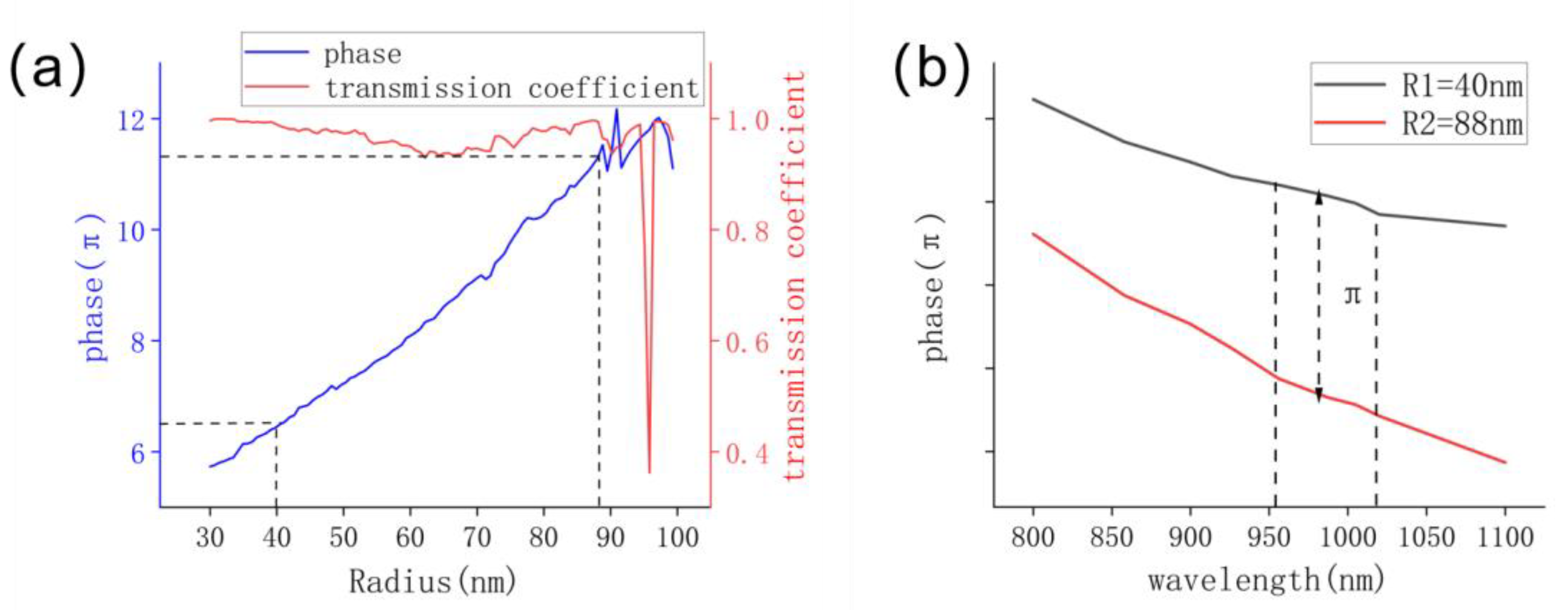
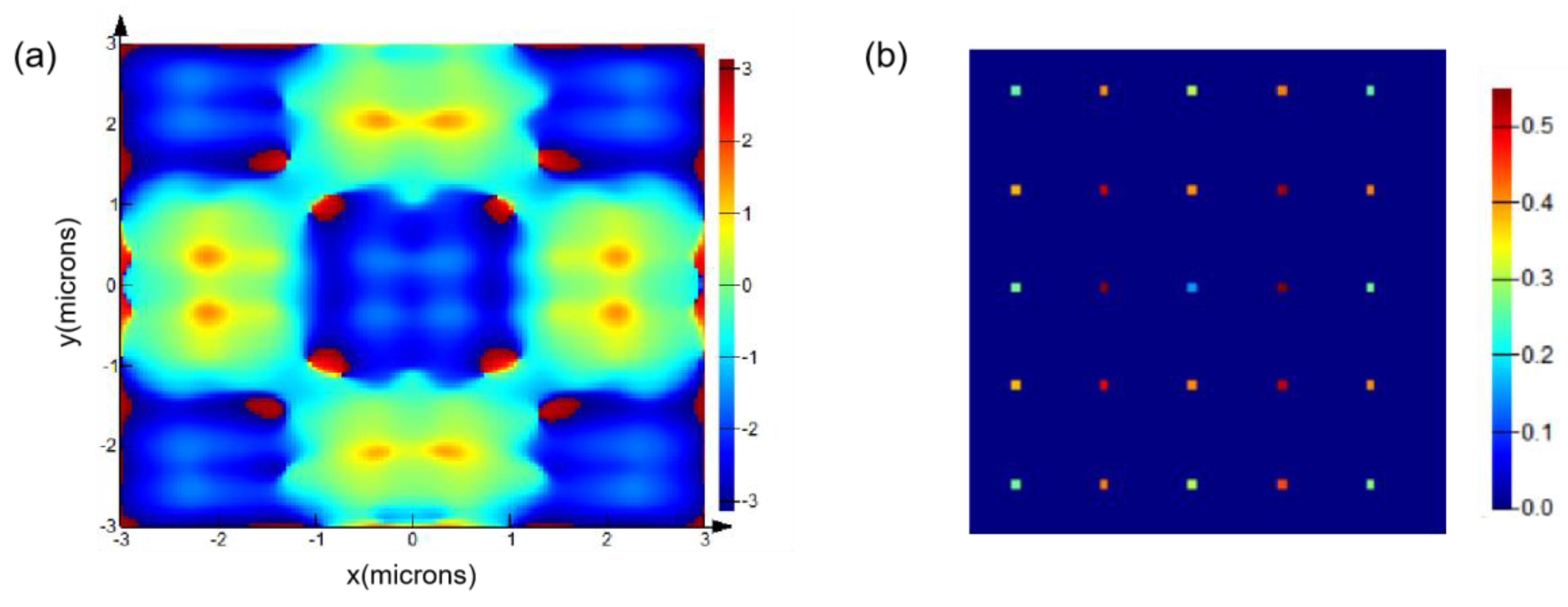
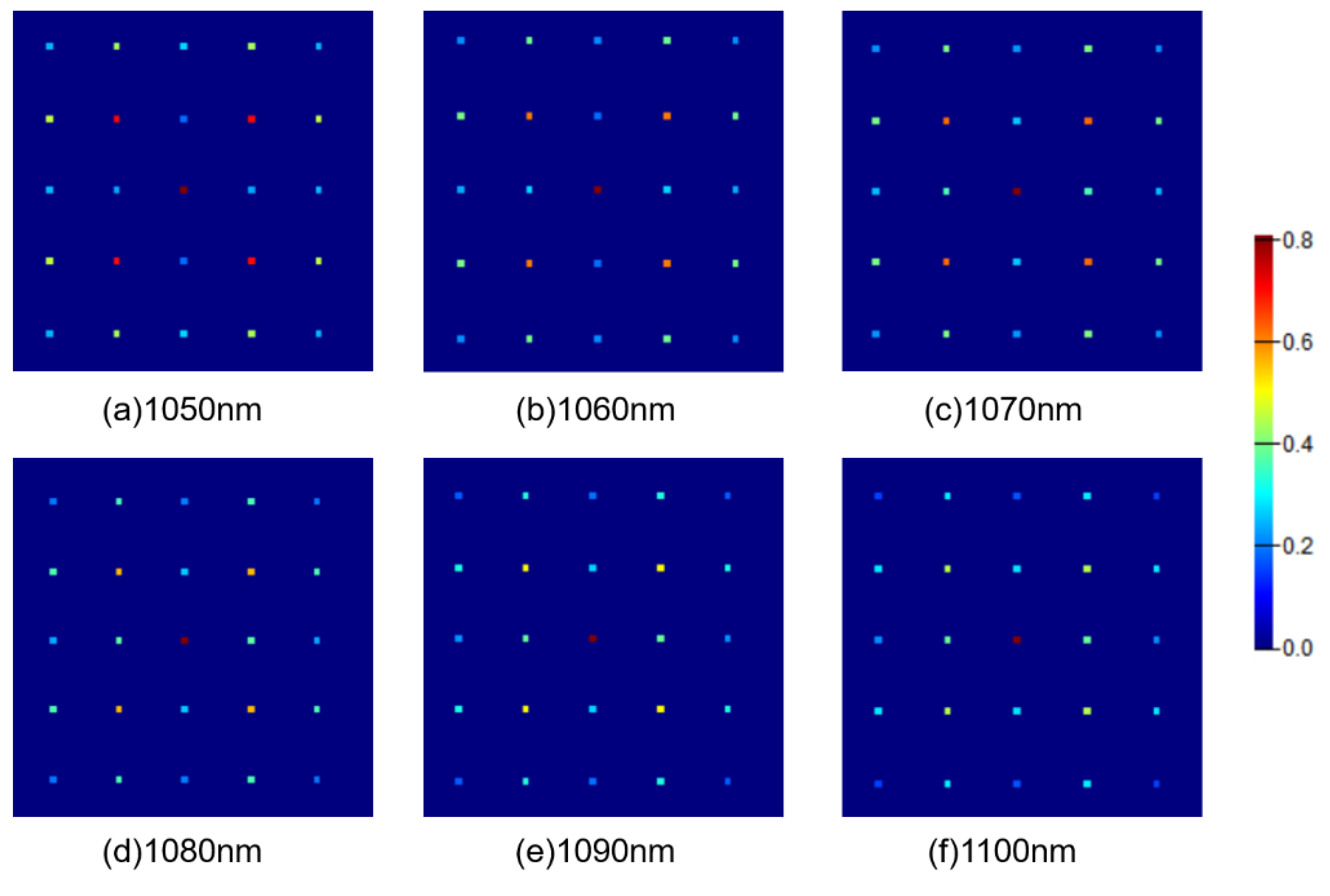
3. Results and Discussion

There are three indexes to evaluate its performance of grating. The first one is the diffraction angle, that is, the angle between two adjacent spots. According to the calculation, the angle between two adjacent spots of the DG is approximately 11°, and the positions of these five points are 0°, ±11°, and ±22°, respectively, which means that the diffraction angle of the DG is 44° × 44°. The second is the conversion efficiency, defined as the ratio of the optical power projected to the target diffraction order to the input power:
η = I 0 + 2 i = 1 N I i
where I0 is the intensity of the central diffraction order, and Ii is the intensity of the I diffraction order.
The third one is the intensity contrast ratio, which is defined as:
C = I max I min I max + I min
where Imax and Imin represent the maximum and minimum optical power of the target diffraction order. The contrast ratio represents the uniformity of the grating spot. A smaller C indicates a better uniformity.
We performed an analysis of the diffraction field at 480–510 nm based on the straight waveguide DG we proposed. First, we exposed it with plane waves of 480–510 nm, which created a nearly uniform diffraction spot of 5 × 5, whose normalized light intensities are shown in Figure 9a–f. It is evident that the distributions of light intensities are uniform between 480 nm and 510 nm. However, results of wavelength between 930 nm and 1020 nm are different, as depicted in Figure 9h-i. Its conversion efficiency can be calculated by Equation (2), which can reach more than 50%; the change of wavelength has little influence on it, and the central stage has a lower intensity than other stages, mainly because of energy loss and the zero-order dark spot phenomenon of grating, which excludes the influence of the middle stage. According to Equation (3), it can be calculated that the contrast ratio is about 40%. More impressively, when the wavelength reaches to 483 nm, the contrast ratio is excellent, close to 20%, as shown in Figure 10.
Similarly, the diffraction field of helical waveguide DG at 950–1020 nm is numerically simulated by using the same method. Figure 11a-f shows its far-field diffraction spot array at different wavelengths, and its far-field diffraction spot is roughly uniform. Compared with Figure 9g–i, the response wave bands for straight and helical waveguides are different, and the conversion efficiency of the helical waveguide is almost zero within the wavelength range of 480–510 nm, as shown in Figure 11f–i. Therefore, we can modulate different working wavelengths of structured light to adapt different scenes by changing the met surface structure using the MBI method. According to Equations (2) and (3), its conversion efficiency and contrast ratio can be calculated, as illustrated in Figure 12. Although its contrast ratio is inferior to the straight waveguide, its conversion efficiency has improved in comparison to the straight one. Due to energy loss and the zero-order dark spot appearance of the grating, the intensity of its central diffraction order is low, so the contrast ratio in Figure 12 is calculated after removing the central diffraction order.
In addition, a comparatively homogeneous spot array can be obtained at the wavelength of 1050–1100 nm by adjusting the height of the straight waveguide to 1500 nm, as shown in Figure 13. The conversion efficiency is about 60%, which is about 10% higher than that at the height of 1000 nm. The contrast ratio is up to 60%, as shown in Figure 14. This is mainly caused by the relatively low intensity of the spot in the corner, resulting from the degradation of energy.
Table 1 lists previous work on DG similar to this work. Although this is not the first time DG based on metasurface has been investigated, most studies have been unable to perform tunable operations. Our proposed DG can be tunable in the range of 480–510 nm and 950–1020 nm. Compared with the previous work, it has a wider range of applications, and has good performance in conversion efficiency and contrast ratio.

4. Conclusions

In summary, we propose a metasurface-based DG, which can flexibly control the phase and effectively form the wavefront. While maintaining high transmittance, different phases can be obtained by adjusting the radius of the nanorods. In this sense, we designed and studied a DG with two radii of LN nanorods and realized the structure adjustment of the nanorods through the MBI method. The straight waveguide DG has a wide working band of 480–510 nm, the conversion efficiency can reach more than 50%, and the contrast ratio is less than 40%. By using MBI, the incidence angle and phase of the beam can be adjusted into a helical waveguide. For helical waveguide DG, the conversion efficiency can reach more than 60% and the contrast ratio is about 40% in the wide operating band of 950–1020 nm. Finally, adjusting the height of the straight waveguide DG can also achieve a change in the operating wavelength, but at the expense of contrast; therefore, there is a trade-off in practical application. The proposed DG has the advantages of tunability, simple fabrication, and multi-wavelength application, and can be widely used in 3D sensing systems.

Author Contributions

Conceptualization, Z.S.; methodology, Y.W. and Y.D.; validation, Y.W. and Z.S.; formal analysis, Y.W. and Z.S.; investigation, Y.W. and H.J.; writing—original draft preparation, Y.W.; writing—review and editing, H.J. and Z.S.; funding acquisition, H.J. and Y.D. All authors have read and agreed to the published version of the manuscript.

Funding

This research was funded by the Guangdong Basic and Applied Basic Research Foundation with grant number 2020A1515010623, the Natural Science Foundation of China with grant number 52175457, 12004080, and 61705046.

Institutional Review Board Statement

Not applicable.

Informed Consent Statement

Informed consent was obtained from all subjects involved in the study.

Data Availability Statement

The data presented in this study are available on request from the corresponding author. The data are not publicly available due to privacy restrictions.

Acknowledgments

This work was supported by the Guangdong Basic and Applied Basic Research Foundation (2020A1515010623), and the Natural Science Foundation of China (52175457, 12004080, and 61705046).

Conflicts of Interest

The authors declare no conflict of interest.

References

  1. Wang, W.-X.; Zhou Fang Wan, Y.-L.; Ning, H.-S. A Survey of Metaverse Technology. Chin. J. Eng. 2022, 44, 744–756. [Google Scholar]
  2. Geng, J. Structured-Light 3d Surface Imaging: A Tutorial. Adv. Opt. Photonics 2011, 3, 128–160. [Google Scholar] [CrossRef]
  3. Ganapathi, V.; Plagemann, C.; Koller, D.; Thrun, S. Real Time Motion Capture Using a Single Time-of-Flight Camera. In Proceedings of the 2010 IEEE Computer Society Conference on Computer Vision and Pattern Recognition, San Francisco, CA, USA, 13–18 June 2010; pp. 755–762. [Google Scholar]
  4. Guo, J.; Gu, F.; Ye, Y.; Song, Z. A Speckle 3d Reconstruction System Based on Binocular Endoscope. J. Integr. Technol. 2021, 11, 13–26. [Google Scholar]
  5. Wu, R.; Zhao, S.; Zhao, Y.; Xie, F. Fringe Projection Profilometry for 3d Measurement of Objects with Different Depth of Fields. Infrared Laser Eng. 2022, 51, 20220088. [Google Scholar]
  6. Li, Y.; Qian, J.; Feng, S.; Chen, Q.; Zuo, C. Deep-Learning-Enabled Dual-Frequency Composite Fringe Projection Profilometry for Single-Shot Absolute 3d Shape Measurement. Opto-Electron. Adv. 2022, 5, 210021. [Google Scholar] [CrossRef]
  7. Li, S.; Han, L.; Dong, P.; Sun, W. Algorithm for Measuring the Outer Contour Dimension of Trucks Using Uav Binocular Stereo Vision. Sustainability 2022, 14, 14978. [Google Scholar] [CrossRef]
  8. Tang, Y.; Zhou, H.; Wang, H.; Zhang, Y. Fruit Detection and Positioning Technology for a Camellia Oleifera C. Abel Orchard Based on Improved Yolov4-Tiny Model and Binocular Stereo Vision. Expert Syst. Appl. 2023, 211, 118573. [Google Scholar] [CrossRef]
  9. Yu, N.; Genevet, P.; Kats, M.A.; Aieta, F.; Tetienne, J.-P.; Capasso, F.; Gaburro, Z. Light Propagation with Phase Discontinuities: Generalized Laws of Reflection and Refraction. Science 2011, 334, 333–337. [Google Scholar] [CrossRef] [Green Version]
  10. Chen, H.T.; Taylor, A.; Yu, N. A Review of Metasurfaces: Physics and Applications. Rep. Prog. Phys. 2016, 764, 7901. [Google Scholar] [CrossRef] [Green Version]
  11. Cai, T.; Wang, G.; Tang, S.; Xu, H.; Duan, J.; Guo, H.; Guan, F.; Sun, S.; He, Q.; Zhou, L. High-Efficiency and Full-Space Manipulation of Electromagnetic Wave Fronts with Metasurfaces. Phys. Rev. Appl. 2017, 8, 034033. [Google Scholar] [CrossRef]
  12. Hisao, K.; Toyota, H.; Yu, W. Optical Elements with Subwavelength Structured Surfaces. Opt. Rev. 2003, 10, 63–73. [Google Scholar]
  13. Li, Z.; Zheng, G.; He, P.; Li, S.; Deng, Q.; Zhao, J.; Ai, Y. All-Silicon Nanorod-Based Dammann Gratings. Opt. Lett. 2015, 4285, 40–48. [Google Scholar] [CrossRef] [PubMed]
  14. Yang, S.; Li, C.; Liu, T.; Da, H.; Feng, R.; Tang, D.; Sun, F.; Ding, W. Simple and Polarization-Independent Dammann Grating Based on All-Dielectric Nanorod Array. J. Opt. 2017, 19, 095103. [Google Scholar] [CrossRef]
  15. Chen, K.; Wang, Y.; He, T.; Cui, Y.; Tao, J.; Li, Z.; Zheng, G. Metasurface Fan-out Diffractive Optical Elements. J. Appl. Opt. 2019, 40, 306. [Google Scholar]
  16. Ni, Y.; Chen, S.; Wang, Y.; Tan, Q.; Xiao, S.; Yang, Y. Metasurface for Structured Light Projection over 120 Degrees Field of View. Nano Lett. 2020, 6719, 20–24. [Google Scholar]
  17. Zheng, X.; Yang, J.; Wang, R.; Lan, T. Visible Light Waveband Dammann Grating Based on All-Dielectric Metasurface. Appl. Opt. 2022, 2184, 61–91. [Google Scholar] [CrossRef]
  18. Ye, Z.; Liu, W.; Sun, P.; Jin, G.; Li, J.; Xie, Y.; Zhou, C.; Jia, W. Equilateral Triangle Hexagonal Array by Crossing Two One-Dimensional Dammann Gratings with 60°. Microw. Opt. Technol. Lett. 2021, 2297, 63–302. [Google Scholar] [CrossRef]
  19. Li, Z.; Dai, Q.; Mehmood, M.; Hu, G.; Yanchuk, B.; Tao, J.; Hao, C.; Kim, I.; Jeong, H.; Zheng, G.; et al. Full-Space Cloud of Random Points with a Scrambling Metasurface. Light Sci. Appl. 2018, 7, 63. [Google Scholar] [CrossRef]
  20. Song, X.; Huang, L.; Tang, C.; Li, J.; Li, X.; Liu, J.; Wang, Y.; Zentgraf, T. Selective Diffraction with Complex Amplitude Modulation by Dielectric Metasurfaces. Adv. Opt. Mater. 2018, 6, 1701181. [Google Scholar] [CrossRef]
  21. Zhang, H.; Zhang, Z.; Song, X.; Zhao, R.; Jia, D.; Liu, T. Tunable Multi-Wavelength Optofluidic Dammann Grating with Beam Splitting Property. Opt. Express. 2021, 29, 33414–33423. [Google Scholar] [CrossRef]
  22. Carletti, L.; Zilli, A.; Moia, F.; Toma, A.; Finazzi, M.; De Angelis, C.; Neshev, D.; Celebrano, M. Steering and Encoding the Polarization of the Second Harmonic in the Visible with a Monolithic Linbo(3) Metasurface. ACS Photonics 2021, 8, 731–737. [Google Scholar] [CrossRef] [PubMed]
  23. Bartal, G.; Cohen, O.; Buljan, H.; Fleischer, J.; Manela, O.; Segev, M. Brillouin-Zone Spectroscopy of Nonlinear Photonic Lattices. In Proceedings of the 2005 Quantum Electronics and Laser Science Conference, Baltimore, MD, USA, 22–27 May 2005. [Google Scholar]
  24. Jin, W.; Yan, L.X.; Jiang, D. Area Scalable Optically Induced Photorefractive Photonic Microstructures. Opt. Mater. 2016, 57, 174–178. [Google Scholar] [CrossRef]
  25. Xavier, J.; Boguslawski, M.; Rose, P.; Joseph, J.; Denz, C. Reconfigurable Optically Induced Quasicrystallographic Three-Dimensional Complex Nonlinear Photonic Lattice Structures. Adv. Mater. 2010, 22, 356–360. [Google Scholar] [CrossRef]
  26. Xia, S.; Jukic, D.; Wang, N.; Smirnova, D.; Smirnov, L.; Tang, L.; Song, D.; Szameit, A.; Leykam, D.; Xu, J.; et al. Nontrivial Coupling of Light into a Defect: The Interplay of Nonlinearity and Topology. Light Sci. Appl. 2020, 9, 147. [Google Scholar] [CrossRef]
  27. Sun, K.; Tan, D.; Fang, X.; Xia, X.; Lin, D.; Song, J.; Lin, Y.; Liu, Z.; Gu, M.; Yue, Y.; et al. Three-Dimensional Direct Lithography of Stable Perovskite Nanocrystals in Glass. Science 2022, 375, 307–310. [Google Scholar] [CrossRef]
  28. Shi, Z.; Li, H.; Zhu, X. Necklacelike Solitons Formed by Manipulating Vortex Beams in a Synthetic Structure. J. Opt. Soc. Am. B 2019, 36, 2007–2012. [Google Scholar] [CrossRef]
  29. Shi, Z.; Preece, D.; Zhang, C.; Xiang, Y.; Chen, Z. Generation and Probing of 3d Helical Lattices with Tunable Helix Pitch and Interface. Opt. Express. 2019, 27, 121–131. [Google Scholar] [CrossRef] [PubMed]
  30. Jiang, H.; Peng, K.; Cui, Y.; Zhong, J.; Zhang, H.; Jiang, Y.; Zhao, W. Design and Simulation of a Gst-Based Metasurface with Strong and Switchable Circular Dichroism. Opt. Lett. 2022, 47, 1907–1910. [Google Scholar] [CrossRef]
  31. Jiang, H.; Zhu, W.; Huang, J.; Zhang, H.; Zhao, W. Active Metasurface in the near-Infrared Region by Gating Ultrathin Tin Films. Opt. Lett. 2022, 5072, 47–75. [Google Scholar] [CrossRef]
  32. Zhang, D.; Ren, M.; Wu, W.; Gao, N.; Yu, X.; Cai, W.; Zhang, X.; Xu, J. Nanoscale Beam Splitters Based on Gradient Metasurfaces. Opt. Lett. 2018, 43, 267–270. [Google Scholar] [CrossRef]
  33. Gao, B.; Ren, M.; Wu, W.; Hu, H.; Cai, W.; Xu, J. Lithium Niobate Metasurfaces. Laser Photonics Rev. 2019, 13, 1800312. [Google Scholar] [CrossRef] [Green Version]
  34. Ma, J.; Xie, F.; Chen, W.; Chen, J.; Wu, W.; Liu, W.; Chen, Y.; Cai, W.; Ren, M.; Xu, J. Nonlinear Lithium Niobate Metasurfaces for Second Harmonic Generation. Laser Photonics Rev. 2021, 15, 2000521. [Google Scholar] [CrossRef]
  35. Fedotova, A.; Younesi, M.; Sautter, J.; Vaskin, A.; Lochner, F.; Steinert, M.; Geiss, R.; Pertsch, T.; Staude, I.; Setzpfandt, F. Second-Harmonic Generation in Resonant Nonlinear Metasurfaces Based on Lithium Niobate. Nano Lett. 2020, 20, 8608–8614. [Google Scholar] [CrossRef] [PubMed]
  36. Fang, B.; Li, H.; Zhu, S.; Li, T. Second-Harmonic Generation and Manipulation in Lithium Niobate Slab Waveguides by Grating Metasurfaces. Photonics Res. 2020, 8, 1296–1300. [Google Scholar] [CrossRef]
  37. Bartal, G.; Cohen, O.; Buljan, H.; Fleischer, J.; Manela, O.; Segev, M. Brillouin Zone Spectroscopy of Nonlinear Photonic Lattices. Phys. Rev. Lett. 2005, 1639, 9402. [Google Scholar]
  38. Wu, X.; Hao, Z.; Bo, F.; Zhang, G.; Xu, J. Advances in Second-Order Nonlinear Optical Effects of Lithium Niobate Micro/Nano Waveguides. Chin. Sci. Bull. 2022, 67, 3915–3927. [Google Scholar]
  39. Jin, G. Binary Optics. Phys. Eng. 2000, 5, 2–5+16. [Google Scholar]
  40. Moreno, I.; Davis, J.; Cottrell, D.; Zhang, N.; Yuan, X.C. Encoding Generalized Phase Functions on Dammann Gratings. Opt. Lett. 2010, 1536, 35–38. [Google Scholar] [CrossRef]
  41. Dammann, H.; Klotz, E. Coherent Optical Generation and Inspection of Two-Dimensional Periodic Structures. Opt. Acta Int. J. Opt. 2010, 24, 505–515. [Google Scholar] [CrossRef]
  42. Fano, U. Effects of Configuration Interaction on Intensities and Phase Shifts. Phys. Rev. 1961, 1866, 124–178. [Google Scholar] [CrossRef]
Figure 1. Transmittance distribution of a 1D DG.
Photonics 10 00141 g001
Figure 2. (a) Curve of phase change and transmittance of the straight waveguide as the radius R of the waveguide from 100 nm to 200 nm. (b) The transmission phase difference of the straight waveguide with two radii of R1 = 140 nm and R2 = 183 nm with a plane wave.
Photonics 10 00141 g002
Figure 3. (a) Top view of straight waveguide nanorod unit. (b) DG metasurface with two sizes of LN straight waveguide nanorods R1 = 140 nm and R2 = 183 nm on the silica substrate. (c) Structure diagram of the unit nanorod with size C = 600 nm and height H = 1000 nm. (d) The planform of straight waveguide DG metasurface.
Photonics 10 00141 g003
Figure 4. (a) Electric field phase distribution of Ex of the transmitted field in the xy plane. (b) Normalized diffractive intensity distribution in the far−field of the straight waveguides DG with two radii of R1 = 140 nm and R2 = 183 nm with x−pol light incident. The color bars show the phase and intensity distribution change in (a,b), respectively.
Photonics 10 00141 g004
Figure 5. (a) Top view of the helical waveguide nanorod cell. (b) DG metasurface with two sizes of LN helical waveguide nanorod R1 = 40 nm and R2 = 88 nm on the silica substrate. (c) Structure diagram of the unit nanorod with size C = 600 nm and height H = 1000 nm. (d) The planform of helical waveguide DG metasurface.
Photonics 10 00141 g005
Figure 6. (a) Curve of phase change and transmittance of the helical waveguide as the radius R of the helix varies from 100 nm to 200 nm. (b) The transmission phase difference of the helical waveguide with two radii of R1 = 40 nm and R2 = 88 nm.
Photonics 10 00141 g006
Figure 7. (a) Phase distributions of Ex of the transmitted field and (b) normalized diffractive intensity distribution in the far−field of the helical waveguide DG with two radii of R1 = 40 nm and R2 = 88 nm with x−pol light incident. The color bars show the phase and intensity distribution change in (a,b), respectively.
Photonics 10 00141 g007
Figure 8. Schematic illustration of 3D sensing system. CL, collimation lens; L, lens.
Photonics 10 00141 g008
Figure 9. (ai) Normalized light intensity distribution of the diffraction spots when plane waves with different wavelengths are incident.
Photonics 10 00141 g009
Figure 10. The conversion efficiency (red, y-axis on the left) and the contrast ratio (blue, y-axis on the right) of DG wavelengths from 480 nm to 510 nm.
Photonics 10 00141 g010
Figure 11. (ai) Normalized light intensity distribution of the diffraction spots when plane waves with different wavelengths are incident.
Photonics 10 00141 g011
Figure 12. The conversion efficiency (red, y-axis on the left) and the contrast ratio (blue, y-axis on the right) of DG wavelengths from 950 nm to 1020 nm.
Photonics 10 00141 g012
Figure 13. (af) Normalized light intensity distribution of the diffraction spots when plane waves with different wavelengths are incident.
Photonics 10 00141 g013
Figure 14. The conversion efficiency (red, y-axis on the left) and the contrast ratio (blue, y-axis on the right) of DG wavelengths from 1050 nm to 1100 nm.
Photonics 10 00141 g014
Table 1. Comparison with previous studies.
PaperWork BandConversion EfficiencyContrast RatioDiffraction Angle
This study480–510 nm, 950–1020 nm>50%, >60%40%44° × 44°
[13]1530–1565 nm50–52%4.67%59° × 59°
[14]1550 nm41.4%50%18° × 18°
[15]633 nmNA24.3%32° × 32°
[16]1550 nm59.1%38.68%120° × 120°
[17]650–690 nm>60%<33%20° × 20°
Disclaimer/Publisher’s Note: The statements, opinions and data contained in all publications are solely those of the individual author(s) and contributor(s) and not of MDPI and/or the editor(s). MDPI and/or the editor(s) disclaim responsibility for any injury to people or property resulting from any ideas, methods, instructions or products referred to in the content.

