Article

Optical Phased Array-Based Laser Beam Array Subdivide Pixel Method for Improving Three-Dimensional Imaging Resolution

1
Beijing Institute of Tracking and Communication Technology, Beijing 100094, China
2
School of Space Information, Space Engineering University, Beijing 101416, China
*
Author to whom correspondence should be addressed.
Photonics 2023, 10(12), 1360; https://doi.org/10.3390/photonics10121360
Submission received: 8 November 2023 / Revised: 27 November 2023 / Accepted: 1 December 2023 / Published: 9 December 2023
(This article belongs to the Special Issue Optical Measurement Systems)

Abstract

:
The small number of pixels in the current linear mode avalanche photodiode (LM-APD) array limits its three-dimensional (3D) imaging resolution. We use an optical phased array-based beam array subdivided pixel method to improve the 3D imaging resolution, using an optical phased array to generate a beam array with the same number of pixels as the LM-APD array and matching positions and controlling each sub-beam in the beam array to scan in the field of view of the corresponding pixel. The sub-beam divergence angle in the beam array is smaller than the instantaneous field of view angle of a single pixel in the LM-APD array. The sub-beam scanning in a single pixel’s field of view realizes the multiple acquisition of the target 3D information by the LM-APD array, thus improving the resolution of the LM-APD array. The distribution of the beam array in the far field is simulated, and the main performance parameters of 3D imaging are analyzed. Finally, a liquid crystal phase modulator is used as an optical phased array device to conduct experiments on a target 20 m away, and the results prove that our method can improve the resolution from 4 × 4 to 8 × 8, which can be improved at least four times.

1. Introduction

Pulsed ranging laser 3D imaging, which emits lasers and acquires 3D information on the target surface according to the flight time of a photon, has been widely used in 3D reconstruction, autonomous driving, relative navigation, etc. [1]. With the increasing number of spacecrafts in space, there is an urgent need for 3D imaging means to observe the state of target spacecraft for the purpose of fault diagnosis and feature identification. A laser 3D imaging system using the LM-APD array as detectors (LM-APD array 3D imaging) could rapidly acquire 3D information about a target. With the advantages of an all-solid-state structure, a low operating voltage, a high frame rate, long-distance imaging and no dependence on ambient light, it is very suitable for the applications that require a limited volume, low power consumption, long imaging distance and high accuracy, such as the 3D imaging of space targets.
Research on laser 3D imaging of non-cooperative targets in space has started in recent years. The German Rendezvous and Docking Sensors (RVSs) pulsed scanning lidar is used for 3D imaging to acquire relative attitude information between the imaging system and the target after more than 40 on-orbit tests [2]. The DragonEye lidar from Advanced Scientific Concepts (ASC) (USA, Goleta), employing the LM-APD array, has been used as the primary sensor for autonomous rendezvous and docking attitude measurements for more than 10 successful autonomous rendezvous missions with the ISS since 2012 [3,4]. NASA’s Origins Spectral Interpretation Resource Identification Security Regolith Explorer (OSIRIS-REX) also uses DragonEye to achieve autonomous rendezvous attitude measurements with non-cooperating targets of an asteroid [5]. The US CST-100 spacecraft also uses DragonEye as a relative attitude measurement sensor to realize autonomous rendezvous. Sensor Test for Orion Relative navigation Risk Mitigation Vision Navigation System (STORRM VNS) from Ball Aerospace & Technologies Corporation, USA also uses the LM-APD array as a detector and realizes relative attitude measurements for the Orion spacecraft. It can be seen that the imaging system using the LM-APD array as a detector has a promising future in 3D imaging of non-cooperative space targets.
When the system field of view is fixed, the number of pixels greatly limits the spatial resolution of the laser 3D imaging system. The maximum number of pixels of the LM-APD array in the laboratory has reached 256 × 256, but that of the commercial LM-APD array is only 16 × 16, which is too low for space target 3D imaging applications. Improvement of the spatial resolution of 3D imaging with a small LM-APD array is a hot research issue. Fiber coupling, image fusion and mechanical scanning methods can help a lot. The main idea of the fiber coupling method is to use the fiber-optic arrays in the image plane instead of the LM-APD array [6,7], but the frame rate is seriously limited; it usually needs 30 s to obtain a frame [8], and it is difficult to control volume and perform assembly. The image fusion method obtains high-resolution 3D images by fusing low-resolution 3D images with high-resolution 2D images [9,10], which can help maintain the frame rate, but there are high requirements for target features and complicated algorithms. The mechanical scanning method is the most mature means to improve resolution. Earlier, Richard et al. [11] utilized the APD array with 4 × 4 pixels combined with dual optical wedge scanning to obtain a resolution of 128 × 128. Zhang Y et al. [12] used the double optical wedge scanning method and utilized an APD array with 5 × 5 pixels to realize a resolution of 128 × 128. Sun et al. [13] used Dammann grating to obtain an 8 × 8 beam array matching the APD array to irradiate the target, deflected the echo with a digital micromirror device to realize random sampling, and compressed perception to improve resolution. Li et al. [14] used diffractive optics to generate a 1 × 100 beam array and a 1 × 100 fiber array coupled with an LM-APD array to achieve simultaneous reception of multiple beams, solving the problem of large-scale multi-beam high-precision transceiver matching, finally obtaining 80 × 1200 3D imaging through 2D mechanical scanning of the platform. Chen et al. [15] used array detectors combined with 1D coaxial scanning to realize the vehicle-mounted platform fast terrain 3D imaging. In Kang et al. [16], based on 32 × 32 SPAD arrays and diffractive optics to build a transceiver common optical path scanning 3D imaging experimental system, spatial resolution was improved by four times. Xie et al. [17] used mechanical micro-scanning to improve APD array resolution from 32 × 32 to 64 × 64. Mechanical scanning is an effective method to improve the 3D imaging resolution of the APD array, but previous methods have scanned the field of view rather than the pixels; the uneven distribution of scanning lines causes the uneven density of the point cloud and the mechanical scanning hysteresis angle has some impact on the imaging quality. It also suffers from problems such as larger volume and higher power consumption. It can be seen that the method to improve the 3D imaging resolution of LM-APD arrays with high efficiency and miniaturization has high research significance and application value.
In response to the problem of low 3D imaging resolution caused by the limited pixels in the current LM-APD arrays, we propose a method to improve the 3D imaging resolution by subdividing the pixel with a beam array based on an optical phased array. First, we present the fundamentals and advantages. Then, we establish the distribution model of the beam array in the far field; the correspondence between the far field distribution of the beam array and the phase modulation parameters of the optical phased array is obtained and a fast design method for modulation parameters of the optical phased array with cascade modulation is proposed to simultaneously realize the generation and scanning of beam arrays on one single-phase modulation device. The number and arrangement of sub-beams in the beam array is consistent with that of the LM-APD array. The divergence angle of each sub-beam is smaller than that of the corresponding LM-APD pixel field-of-view angle, and each sub-beam scans within the corresponding LM-APD pixel field of view, thus completing the subdivision of each pixel field of view, ultimately realizing high-resolution 3D images. Then, we analyze the effects and limitations of our method for improving the 3D imaging performance of LM-APD arrays. Finally, 3D imaging experiments are conducted on a diffusely reflecting target at 20 m, which improves the spatial resolution of system by a factor of four.

2. Methods

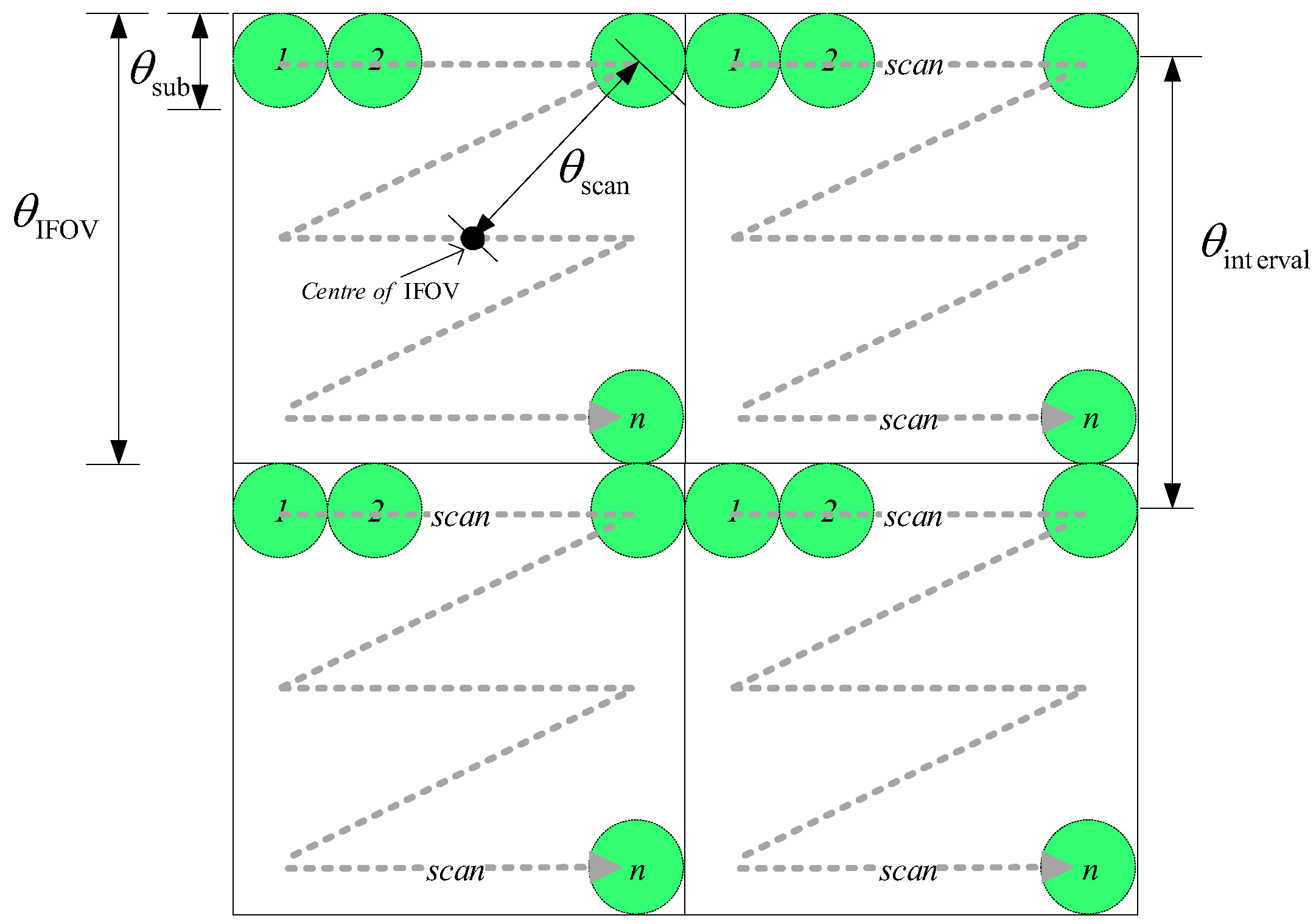
2.1. Fundamentals of the Beam Array Scanning Method for Improving Spatial Resolution

Each pixel of the LM-APD array is independent of each other and the crosstalk is very low, the signal received by each pixel does not affect the surrounding pixels, i.e., each pixel of the LM-APD array can be regarded as an independent 3D imaging unit, and the field of view (FOV) of each pixel can be equated to an independent instantaneous FOV, and each pixel can receive and respond to the laser echo signal only in its corresponding instantaneous FOV [18,19].
Utilizing this characteristic of LM-APD, we improve the resolution of 3D imaging of the LM-APD array by beam array scanning, which generates beam arrays that match the number and distribution of pixels in the LM-APD array, Figure 1 shows the schematic diagram of resolution improvement after the beam array scans in the corresponding LM-APD array FOV. The three diagrams on the left show that when the beam array is deflected at different angles from 1, 2, to n , the sub-beams point to different regions of the instantaneous FOV of the corresponding LM-APD pixels, and the time of flight (TOF) of the photons in the sub-beams to return to the corresponding LM-APD pixel is the relative distance to the corresponding region to which the sub-beams are pointing. Each sub-beam scans multiple times simultaneously in the instantaneous FOV of the corresponding pixel, and the corresponding TOF of the photons is recorded independently for each pixel, realizing subdivided multiple sampling of each pixel to improve the spatial resolution of the LM-APD array by subdividing the instantaneous field of view of the pixel. The right side of Figure 1 shows that the 3D imaging resolution of the LM-APD array can be improved by storing the data acquired in each scan according to the deflection angle at the time of scanning after multiple scans.
As shown in Figure 2, assuming that the instantaneous FOV angle of the pixel in the LM-APD array is θ IFOV and the divergence angle of each sub-beam in the beam array is θ sub , our method can maximally increase the number of sampling points by θ IFOV 2 / θ sub 2 times, which means that the spatial resolution of 3D imaging can be increased by θ IFOV 2 / θ sub 2 times. This method allows the beam array to scan simultaneously at each pixel, and the efficiency improvement over single-beam scanning of the unit detector is a multiple of the number of pixels n APD × n APD , which effectively reduces the scanning time. Since the beam array and the LM-APD array transmit and receive coaxially, and the angle between the sub-beams θ interval is equal to the instantaneous FOV angle of the LM-APD pixel, the coaxial matching relationship between the beam array and the LM-APD array will not be changed with the change in the target distance.
The key technology required to realize beam array scanning is divided into two steps: beam array generation and beam array scanning. Single beam splitting into beam array has a variety of realization methods, such as microlens array, fiber coupling, diffractive elements, etc., but these methods still need to cooperate with other methods such as mechanical scanning after beam splitting in order to realize beam array scanning, which increases the complexity of the beam array scanning method. We previously [20] tried to use Dammann grating to realize beam splitting, and combined it with liquid crystal phase space light modulator scanning to realize the method in this paper. Figure 3 shows the structure schematically; although the generation and scanning of the beam array was realized, the energy efficiency was low and the structure was complicated.
In this paper, a single optical phased array is used to realize the generation and scanning of the beam array simultaneously, as shown in Figure 4, which represents the side view of the system structure. According to the parameters of the received field-of-view angle and the number of pixels, the optical phased array is used to generate the matched beam array, and the deflection direction of the beam array is simultaneously controlled in the same optical phased array, so that each sub-beam that scans simultaneously in the FOV of the corresponding pixel is realized. At the transmitter end, only one optical phased array is used to generate and scan simultaneously, which greatly simplifies the system’s structure.

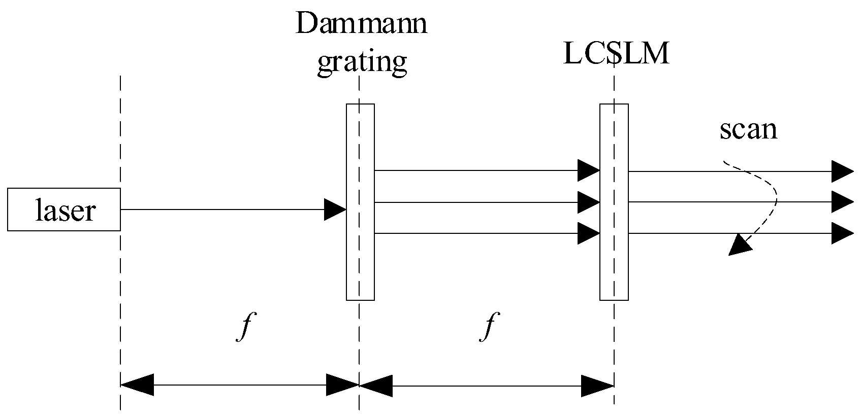
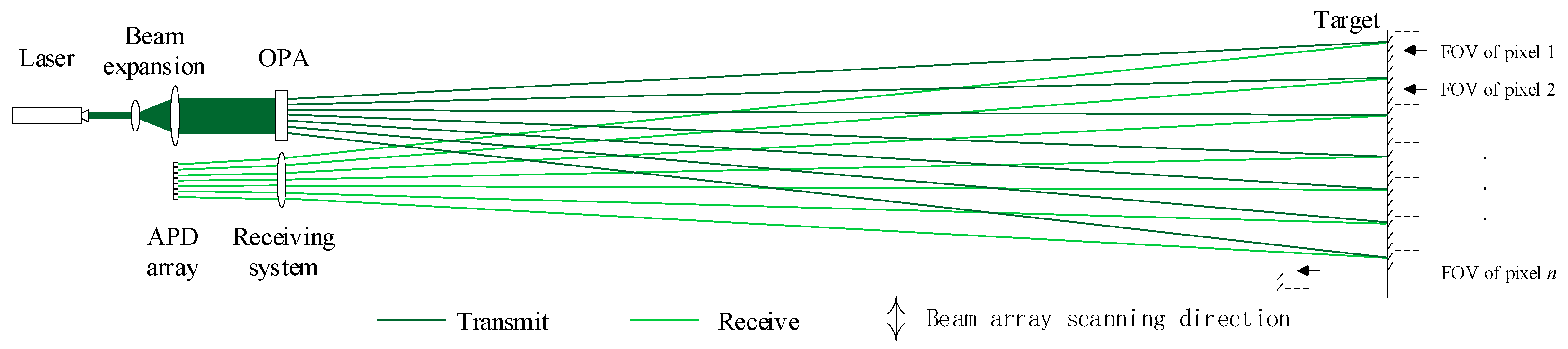
2.2. Optical Phased Array Beam Array Generation and Scanning Methods

The optical phased array beam array control method is based on the theory of diffractive optics, which is widely been used such as on-chip wireless interconnection, etc. [21]. The generation and control of the beam array is realized by loading different modulation phases.

2.2.1. Principle of Optical Phased Array Beam Control

Optical phased arrays modulate the complex amplitude distribution of the incident beam by controlling the phase relationship between each array element. According to the Huygens–Fresnel principle, the near-axis Fresnel diffraction is shown in Equation (1) [22]:
U z ( x z , y z ) = e i 2 π z λ e i π λ z ( x i 2 + y i 2 ) i λ z U 0 ( x 0 , y 0 ) e i π λ z ( x 0 2 + y 0 2 ) e i 2 π λ z ( x 0 x i + y 0 y i ) d x 0 d y 0
where U z ( x z , y z ) is the complex amplitude distribution of the laser in the plane at the distance of z ; U 0 ( x 0 , y 0 ) is the complex amplitude distribution of the laser in the plane at the distance of z = 0 ; and the corresponding spatial frequency of U z ( x i , y i ) is ( x i / λ z , y i / λ z ) . When z π ( x 0 2 + y 0 2 ) / λ , Equation (2) is the corresponding Fourier transform of Equation (1):
U z ( x i , y i ) = e i 2 π z λ e i π λ z ( x i 2 + y i 2 ) i λ z F U 0 ( x 0 , y 0 )
In practice, optical phased arrays typically have spacing between the array elements and are limited in aperture, which results in amplitude modulation as shown in Equation (3):
t A = i = 0 M j = 0 N rect x m d OPA a OPA rect y n d OPA a OPA
where M and N are the array elements number in the directions x and y , respectively; d OPA is the size of the array elements; a OPA is the size of the electrodes in the array elements.
Assuming that the complex amplitude distribution of the incident beam is U in ( x , y ) and the modulation phase of the optical phased array is t OPA , the complex amplitude distribution of the beam after modulation by the optical phased array is as shown in Equation (4):
U 0 ( x 0 , y 0 ) = t A t OPA U in ( x , y )
Combined with Equation (2), the complex amplitude distribution of the emitted beam of the optical phased array at the distance of z is shown in Equation (5).
U z ( x z , y z ) = e i 2 π z λ e i π λ z ( x 1 2 + y 1 2 ) i λ z F t A t OPA U in ( x , y )

2.2.2. Modulation Phase Design

The two main methods for designing the phase of multibeam modulation are the sub-aperture method and cascade modulation. The sub-aperture method is shown in Figure 5a, where the whole optical phased array is divided into a total of n sub-phased arrays s 1 s 2 s n loaded with different modulation phases, each of which is equivalent to an independent phased array, and the independent modulation of each sub-beam is realized by changing the modulation phase of each sub-phased array. The cascade modulation method loads multiple modulation phase matrices on the optical phased array simultaneously, which is equivalent to the beam passing through multiple zero-pitch optical phased arrays in sequence, as shown in Figure 5b.
The sub-beam of the sub-aperture method corresponds to a limited number of array elements in the sub-phased array, while the sub-beam of the cascade modulation method is the joint action of all array elements in the phased array, and the divergence angle of the sub-beam is narrower than that of the sub-aperture method, which can achieve a higher angular resolution. Therefore, the cascade modulation method is adopted, and the modulation phase is shown in Equation (6):
t OPA ( x , y ) = t OPA _ s ( x , y ) t OPA _ g ( x , y )
where t OPA _ g is the beam array generation modulation phase and t OPA _ s is the beam array scanning modulation phase. Equation (7) shows the final beam complex amplitude distribution in the far field:
U z ( x z , y z ) = e i 2 π z λ e i π λ z ( x z 2 + y z 2 ) i λ z F t A ( x , y ) F t OPA _ s ( x , y ) F t OPA _ g ( x , y ) F U in ( x , y )
The intensity distribution of the beam array I z ( x z , y z ) is shown in Equation (8):
I z ( x z , y z ) = F t A ( x , y ) F t OPA _ g ( x , y ) F t OPA _ s ( x , y ) F U in ( x , y ) 2

Beam Array Generation Phase Design

A binary optical approach is used to design beam arrays to generate modulated phases. The design of the 2D beam array generation modulation phase must start in 1D and then expand in 2D. The 1D distribution of the beam array in the far field is determined by the coordinates of the hopping point a l , b l ( l = 1 , 2 L ) in a single cycle, and the modulation phase of a single cycle t OPA _ g x _ s ( x ) in the x-direction is as shown in Equation (9):
t OPA _ g x _ s ( x ) = e i π , o t h e r 1 , a l x b l
A Fourier series expansion of the modulation phase t OPA _ g x _ s ( x ) is performed as Equation (10):
t OPA _ g x _ s ( x ) = T OPA _ g x ( m ) e i 2 π m x
where T OPA _ g x ( m ) is the Fourier transform coefficients of each diffraction level of the Fourier series expansion as shown in Equation (11):
T OPA _ g x ( m ) = 2 l = 1 L ( b l a l ) 1 ,   m = 0 i π m l = 1 L ( e i 2 π m b l e i 2 π m a l ) ,   m 0
When the incident light of the optical phased array is a plane light of unit amplitude, the relative intensity distribution of the generated beam array at each diffraction level in 1D of the far field is as shown in Equation (12):
P OPA _ g x ( m ) = | T OPA _ g x ( m ) | 2
Taking the uniformity and diffraction efficiency of the beam as the evaluation criteria, the objective function E 2 is constructed to calculate the hopping point coordinates, as shown in Equation (13):
E 2 = α P ( 0 ) P E P ( 0 ) 2 + 2 m = 1 P ( m ) P E P ( m ) 2 + ( 1 α ) ( 1 P E ) 2
where α is the weighting parameter of beam uniformity and diffraction efficiency; P ( m ) is the theoretical object value of intensity distribution at all levels; and P E is the sum of diffraction efficiency of beams at all levels. The number of LM-APD array pixels in 1D determine the required beam splitting ratio 1 × n APD , and the coordinates of the hopping point of the generated modulation phase in the direction of x in a single cycle and the 1D distribution of t OPA _ g x _ s ( x ) can be obtained by the iterative optimization of Equation (13) after making m = n . The distribution of t OPA _ g ( x ) in the x-direction t OPA _ g x ( x ) can be obtained by expanding k times of t OPA _ g x _ s ( x ) . Transpose t OPA _ g x ( x ) to obtain the distribution in the y direction t OPA _ gy ( y ) , and the final beam array generation modulation phase t OPA _ g is as shown in Equation (14):
t OPA _ g = t OPA _ g x t OPA _ g y
Then, an n APD × n APD beam array is obtained in the far field.
At the same time, in order to meet the scanning requirements, the angle θ interval between neighboring sub-beams in the beam array needs to be equal to the instantaneous FOV angle of a pixel, as shown in Equation (15):
θ interval = θ FOV / n APD
θ interval is modulated by the physical length of a single cycle d OPA _ g in t OPA _ g . In practice, the size of an optical phased array is fixed, and the corresponding length of a single cycle can only be changed by adjusting the number of expansion cycles in the optical phased array. When n APD is odd, θ interval is equal to the angle between two diffraction stages; when n APD is even, the beam splitting is realized by the removing the even diffraction stages, θ interval is equal to two times of the angle between two diffraction stages, as shown in Equation (16):
θ interval = λ / d OPA _ g ,   n APD = o d d 2 λ / d OPA _ g ,   n APD = e v e n
where λ is the wavelength of the incident light of the optical phased array. Combining Equations (15) and (16), when the FOV is θ FOV , the length of a single cycle in t OPA _ g is as shown in Equation (17):
d OPA _ g = n APD λ / θ FOV ,   n APD = o d d 2 n APD λ / θ FOV ,   n APD = e v e n
When the physical size of the optical phased array is D OPA × D OPA , when combined with Equation (17), the number of extended cycles k g is as shown in Equation (18):
k g = D OPA θ FOV n APD λ ,   n APD = o d d D OPA θ FOV 2 n APD λ ,   n APD = e v e n
When k g cannot be rounded, the phase modulation parameters in the last cycle can be truncated proportionally. In summary, the generated modulation phase t OPA _ g of the beam array is as shown in Equation (19):
t g ( x , y ) = k g = 1 K g rect [ rem ( x d OPA _ g ) b k g + a k g 2 b k g a k g ] + e i π k g = 1 K g 1 rect [ rem ( x d OPA _ g ) a k g + 1 + b k g 2 a k g + 1 b k g ] k g = 1 K g rect [ rem ( y d OPA _ g ) b k g + a k g 2 b k g a k g ] + e i π k g = 1 K g 1 rect [ rem ( y d OPA _ g ) a k g + 1 + b k g 2 a k g + 1 b k g ]
where rem is the residual function.

Beam Array Scanning Phase Design

The beam array scanning is realized by adjusting the phase difference between the array elements in the optical phased array (see Figure 6).
Assuming that the optical phased array is an ideal continuous phased array, i.e., without considering the spacing between the array elements, when the beam array scans at an angle of θ x in the x direction, the modulation phase loaded by the array element with the largest phase delay φ max is as shown in Equation (20):
φ max = e i 2 π D tan θ x λ
And as the delay between neighboring array elements is equidistant, the difference in modulation phase between neighboring array elements Δ φ OPA is as shown in Equation (21):
Δ φ OPA = e i 2 π D OPA tan θ x λ n OPA
Then, the modulation phase of t OPA _ s in the x direction t OPA _ s x is as shown in Equation (22):
t OPA _ s x ( x ) = e i 2 π x D OPA tan θ x λ n OPA
Similarly, the modulation phase of t OPA _ s in y direction t OPA _ s y can be obtained. In summary, the scanning modulation phase t OPA _ s of the beam array is as shown in Equation (23):
t OPA _ s ( x , y ) = e i 2 π ( x D OPA tan θ x λ n OPA + y D OPA tan θ y λ n OPA )
Combining Equations (3), (16) and (20), the modulation phase of the optical phased array finally loaded is as shown in Equation (24):
t OPA ( x , y ) = e i 2 π ( x D OPA tan θ x λ n OPA + y D OPA tan θ y λ n OPA ) k g = 1 K g rect [ rem ( x d OPA _ g ) b k g + a k g 2 b k g a k g ] + e i π k g = 1 K g 1 rect [ rem ( x d OPA _ g ) a k g + 1 + b k g 2 a k g + 1 b k g ] k g = 1 K g rect [ rem ( y d OPA _ g ) b k g + a k g 2 b k g a k g ] + e i π k g = 1 K g 1 rect [ rem ( y d OPA _ g ) a k g + 1 + b k g 2 a k g + 1 b k g ]
By loading the optical phased array with the modulation phase as in Equation (24), the generation and scanning of the beam array can be performed simultaneously after a single beam is incident on the phased array.

3. Simulation and Analysis

3.1. Beam Control Method Simulation

According to Equations (1)–(5), we can simulate and analyze the beam array control method.

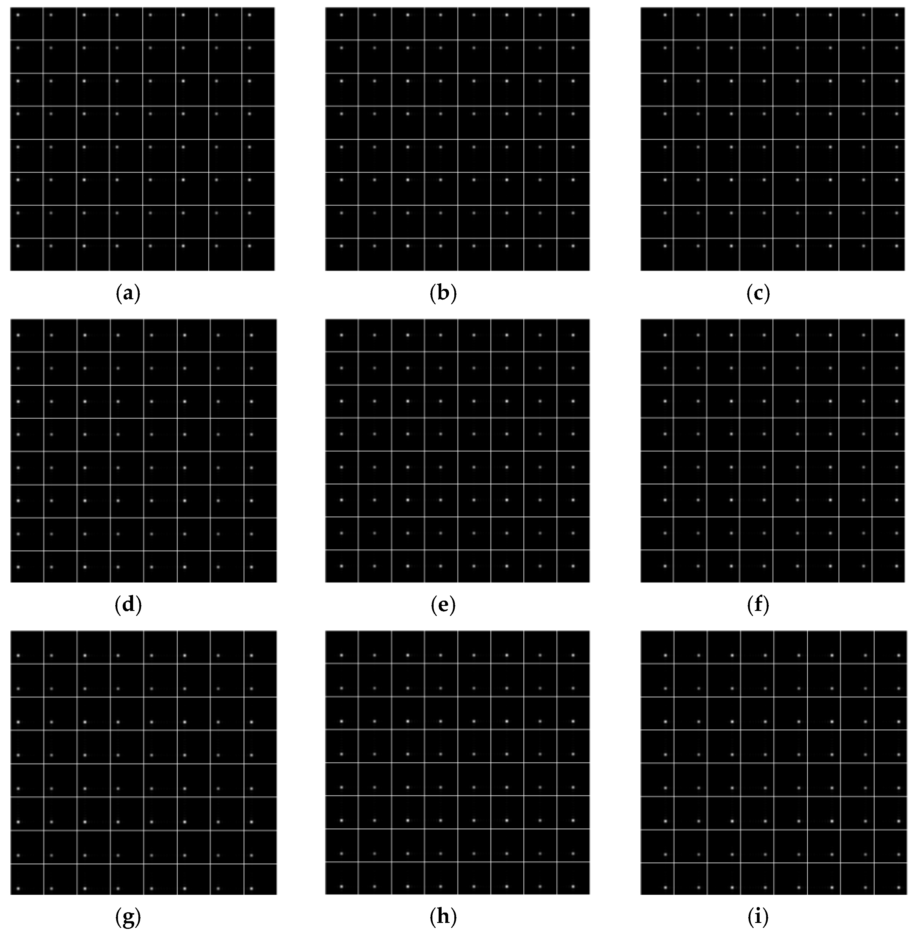
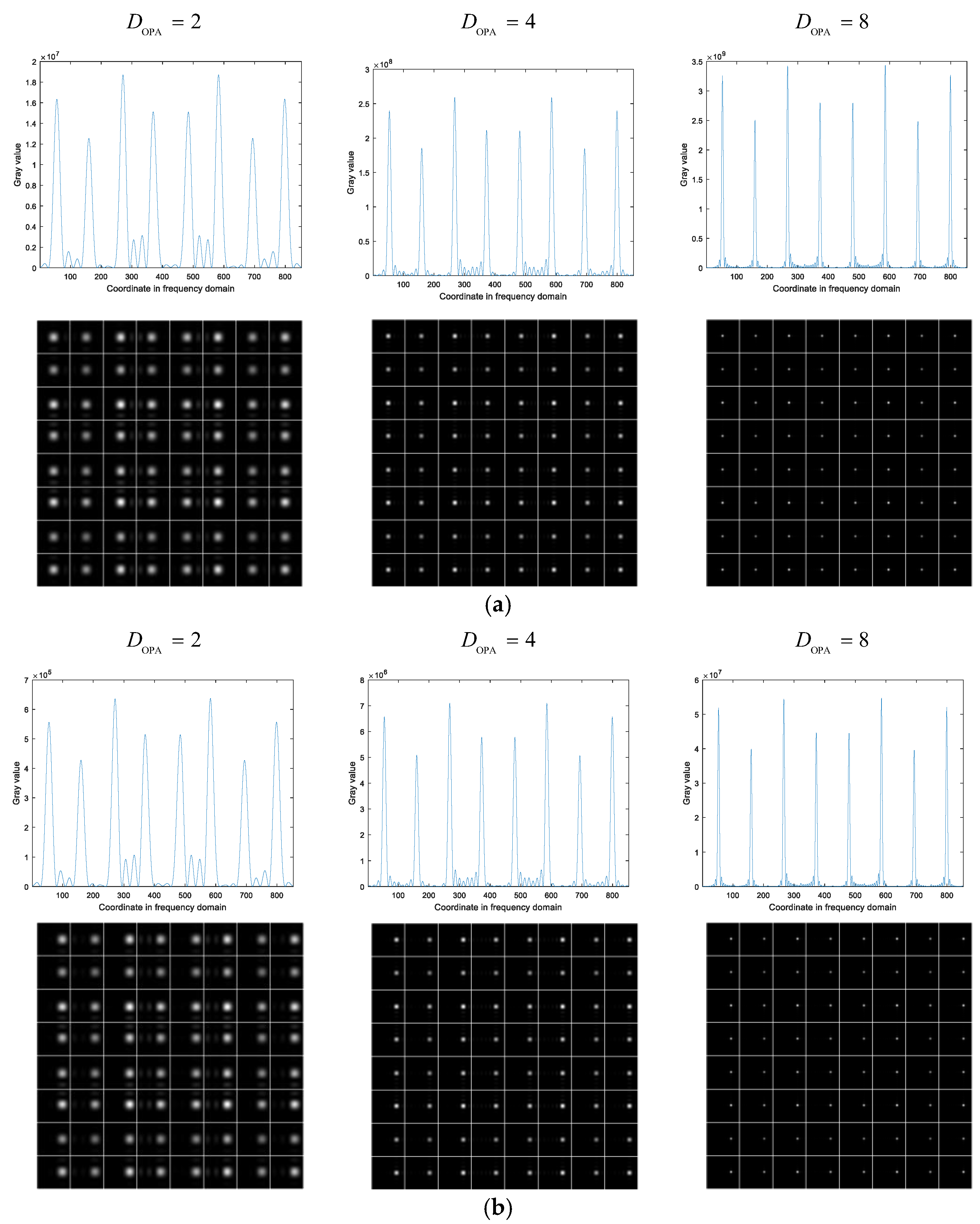
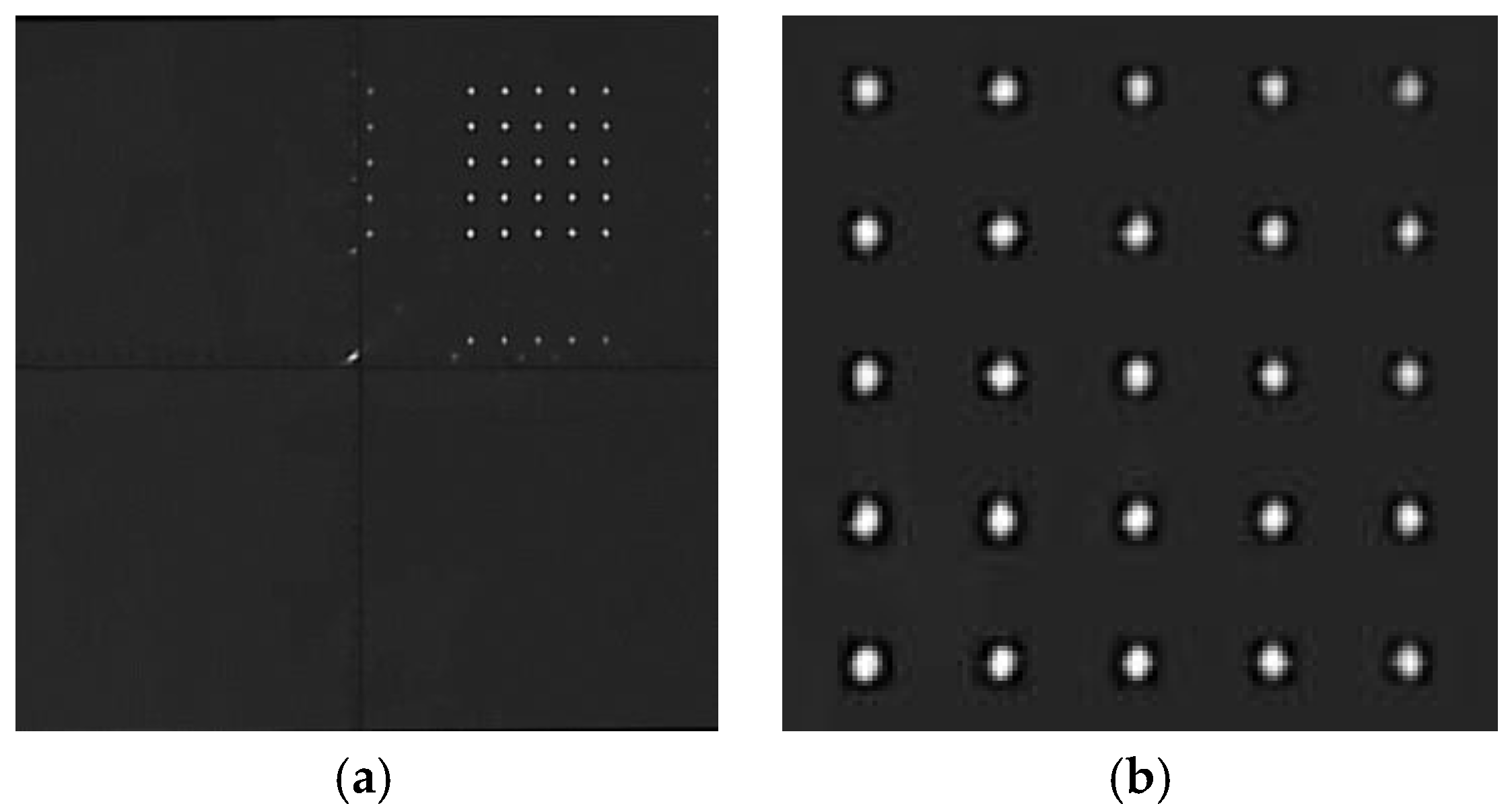
3.1.1. Simulation Results

The scanning of a target at a distance of 10 m was analyzed via simulation, and the corresponding physical parameters are: the pixels of the LM-APD array is 8 × 8, the array elements number of the optical phased array is 720 × 720, the size of a single array element is 6.3 μ m × 6.3 μ m , and the FOV of the receiving optical system is 50 mrad × 50 mrad, which means that the field of view of each pixel is 6.25 mrad × 6.25 mrad.
The spot distributions of the beam array scans at 10 m in 9 angles are shown in Figure 7, and each figure corresponds to a physical size of 0.5 m. The white box lines in the figure are the received FOV ranges of each pixel of the LM-APD.

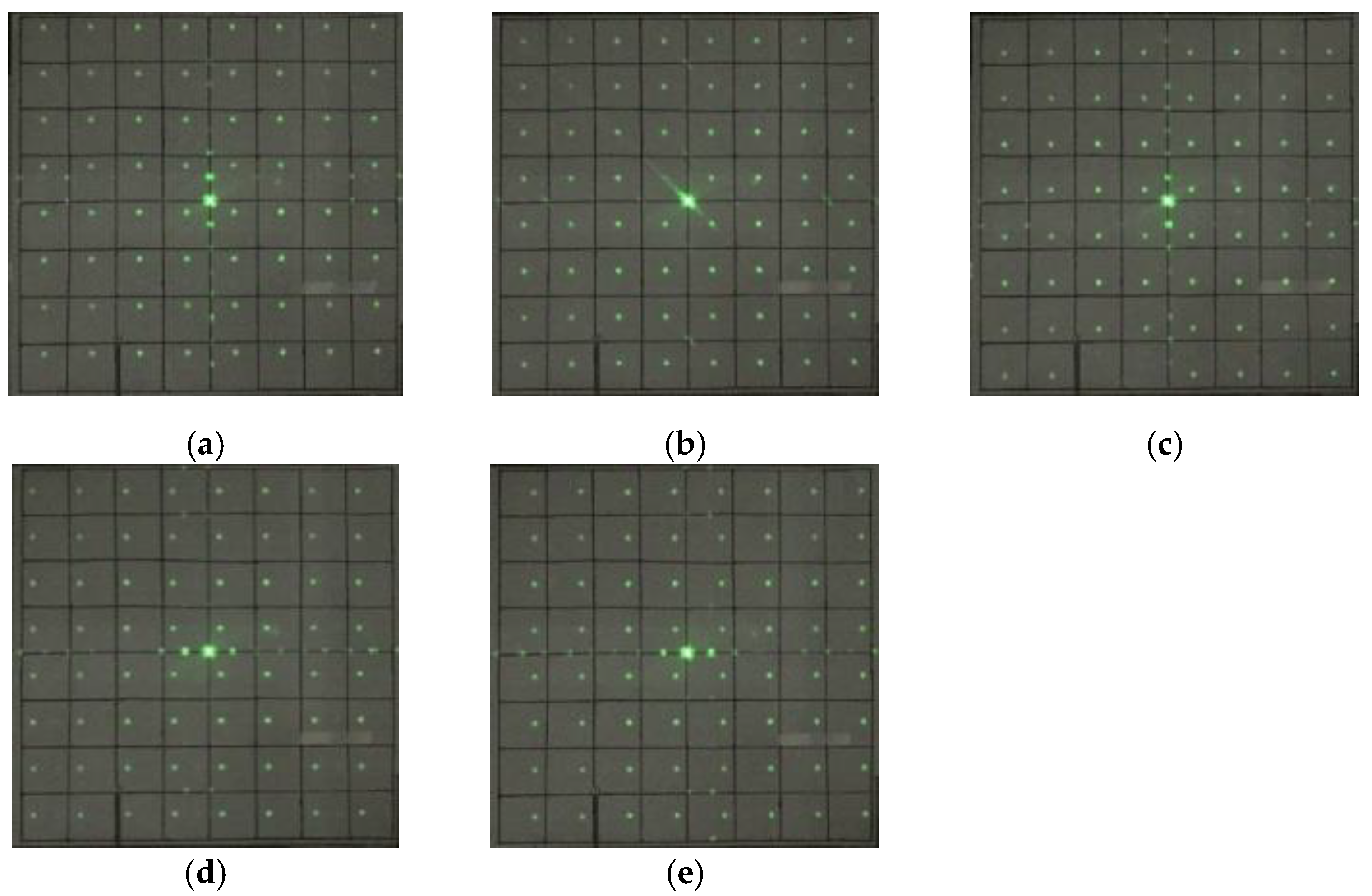
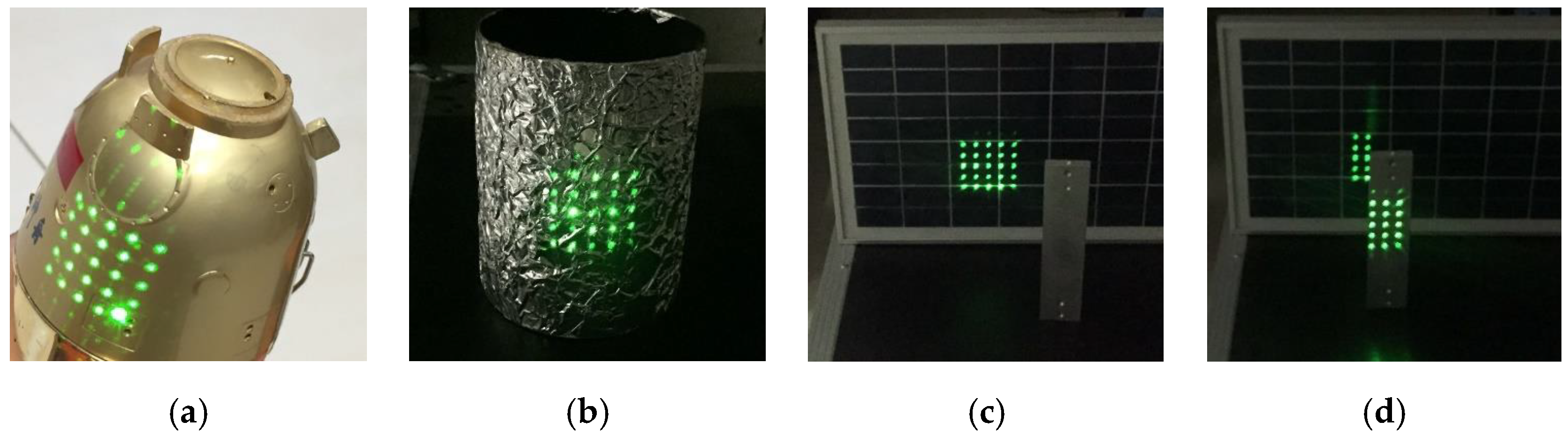
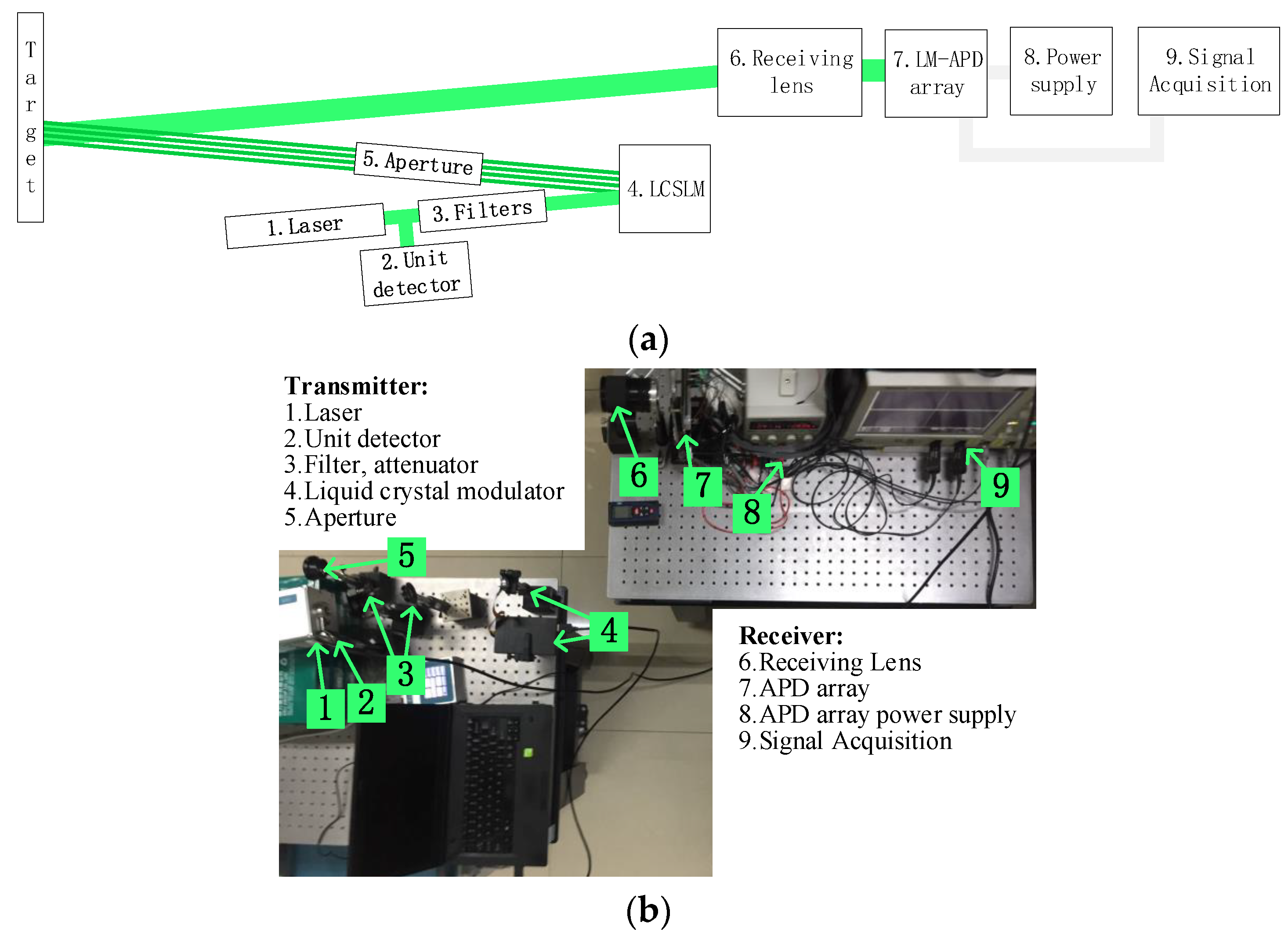
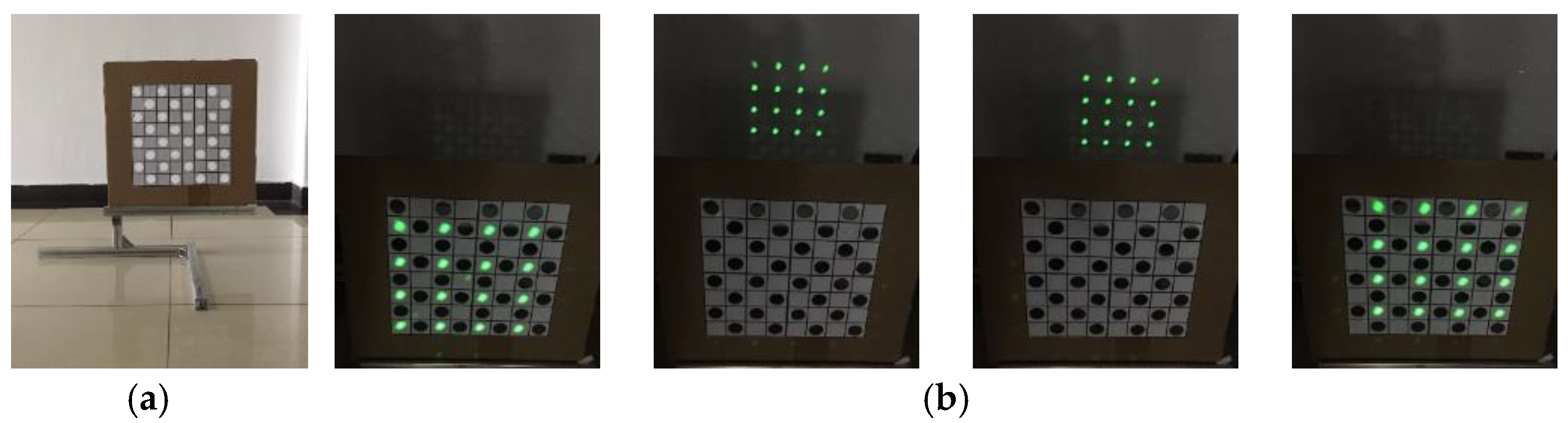
3.1.2. Experiment Results

The liquid crystal modulator is the optical phased array in the experiment, and the receiving end is as shown in Figure 8, which is drawn with a square gird to show the FOV area of the receiving optical system with the FOV of each pixel of the LM-APD array. The total size of the square grid is 50 cm × 50 cm, and the size of each small grid is 6.25 cm × 6.25 cm, i.e., representing the corresponding FOV of each pixel of the 8 × 8 LM-APD array, corresponding to the 50 mrad × 50 mrad of the receiving field of view. When z = 10   m , the beam array distribution in 5 angles is as shown in Figure 8.
The experiment can prove that the distribution of the beam array in the plate at 10 m is consistent with the simulation. However, due to the liquid crystal modulator used in the experiment being a reflective modulator, there are grid-like metal circuit structures on its surface, and these areas are unable to modulate the phase and will instead reflect the beam directly. The simulation ignored the duty cycle of the liquid crystal modulator, so the experiment and the simulation have some differences, for example, the bright spot that appeared in the center of the results. If a transmissive phase modulator is used, a more consistent result with the simulation can be obtained.
The distributions of the beam array on the surface of several other objects are shown in Figure 9. Figure 9c,d show that the distribution of the beam array does not change with the occurrence of partial occlusion, and thus our method will not be limited by the situation of partial occlusion of the target. This characteristic does not change when the number of beams in the beam array changes.

3.2. Performance Analysis

We mainly analyzed the performance improvement and differences in array beam scanning over the original floodlight illumination method from various aspects, including FOV angle, spatial resolution, number of sampling points, beam energy uniformity, energy efficiency and imaging frame rate, which are related to the performance of 3D imaging applications.

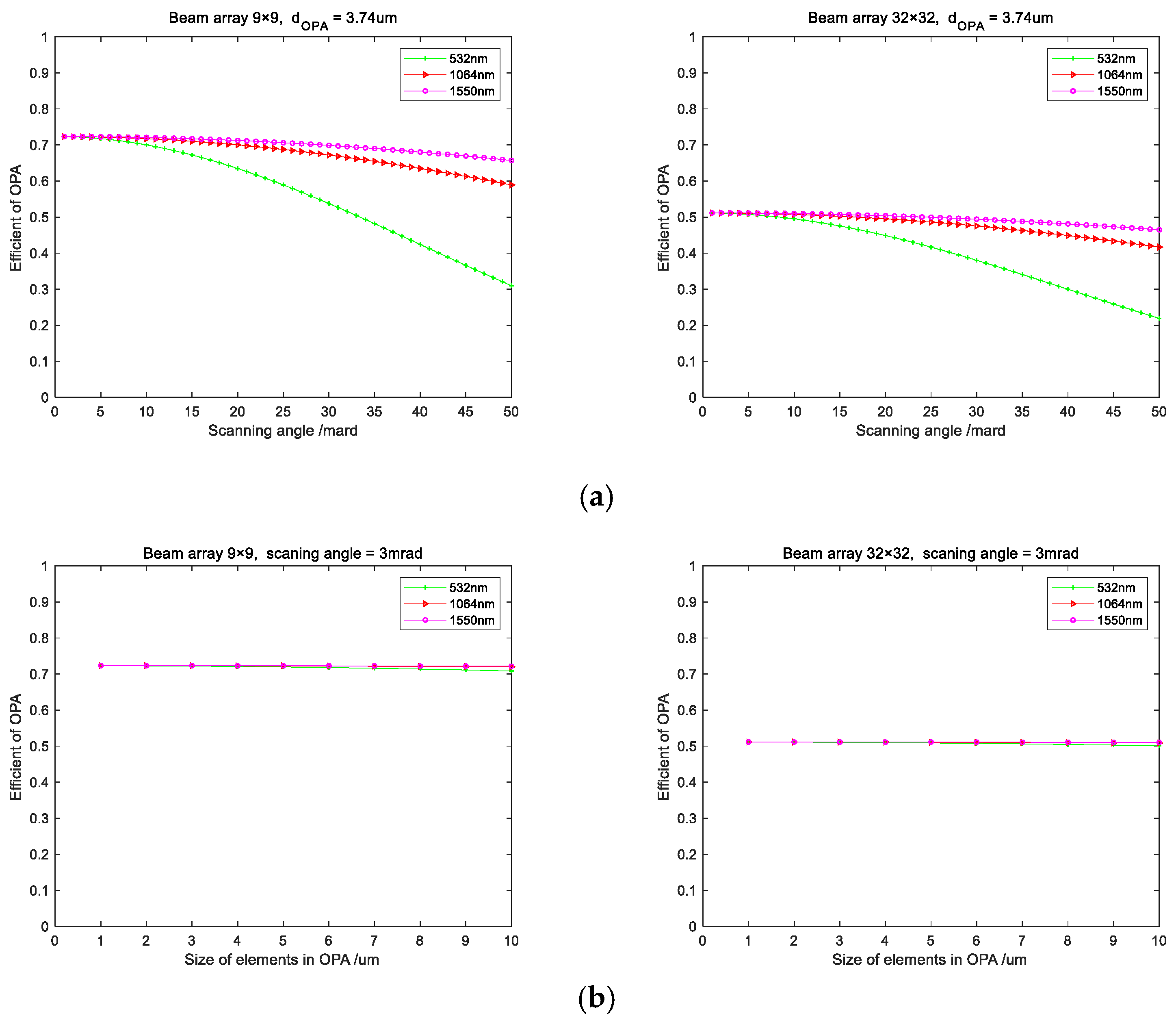
3.2.1. Field of View

The maximum scanning angle θ scan _ max that can be achieved by an optical phased array limits the FOV of system, θ scan _ max is as shown in Equation (25):
θ scan _ max = λ Δ φ OPA _ max 2 π d OPA
where Δ φ OPA _ max is the maximum phase difference between adjacent array elements, typically π .
Equation (25) shows that the maximum scanning angle that can be realized by optical phased arrays is limited, and when designing the system, the received FOV of the LM-APD must satisfy Equation (26):
θ IFOV 2 θ scan _ max
Equations (25) and (26) show that the maximum FOV of the system is as shown in Equation (27):
θ IFOV = 2 2 λ d OPA
Equation (27) shows that for a fixed wavelength, the maximum 3D imaging receptive FOV that can be matched by a beam array is mainly limited by the size of the array elements d OPA , the smaller the array element, the larger the receiving FOV that the beam array can match. The relationship between θ IFOV and d OPA for the three common wavelengths is as shown in Figure 10.
Currently, array element scales of both optical waveguide arrays and liquid crystal modulators can reach the micrometer scale. In long-range 3D imaging application scenarios, the receiving FOV is usually small, and as shown in Figure 10, our method does not limit the receiving field-of-view angle in most cases.

3.2.2. Spatial Resolution

From Equation (8), the complex amplitude distribution of the beam array in the far field is modulated jointly by the incident beam and the phased array transmittance. For a single sub-beam, its far-field spot size is mainly affected by the spot area of the incident beam in the phased array, which is manifested as the convolution of sin c ( D OPA ) and F ( U in ) , i.e., the spread of the incident beam by the effective aperture of optical phased arrays. If the effective aperture of the optical phased array matches the incident beam and the incident beam is a fundamental mode Gaussian distribution, the sub-beam in the beam array is a Gaussian distribution with a divergence angle consistent with the divergence angle of the incident beam, and the optical phased array does not change the divergence angle of the beam. When the size of the optical phased array is larger than the size of the spot incident on the optical phased array, the optical phased array does not further compress the beam, as shown in Figure 11.
Thus, the maximum resolution of 3D imaging is determined by the incident beam divergence angle. Figure 12 shows the variation in beam array distribution in the far field for different optical phased array sizes, and Figure 12a,b show the distribution of spots in the beam array in the far field when the scanning angle is (0 mrad, 0 mrad) and (1.56 mrad, 0 mrad).
Figure 12 shows that the spot size is not affected when the scanning angle is changed; this is because the change in scanning angle is affected by the interference between the individual array elements in the phased array, which is not related to the spot size. It can also be seen from Figure 12 that the sidelobe of the sub-beam decreases with the increase in the size of the optical phased array, because when the cycle length d OPA _ g is fixed, the larger the size of the optical phased array, the more cycles are involved in the modulation, the more the half-angle width of each diffraction stage λ / D OPA decreases, i.e., the sharpness of the diffraction stage increases. Therefore, in order to avoid the effect of sidelobe, if it is necessary to control the resolution of scanning, the method of controlling the divergence angle of the incident beam should be chosen instead of reducing the size of the optical phased array.

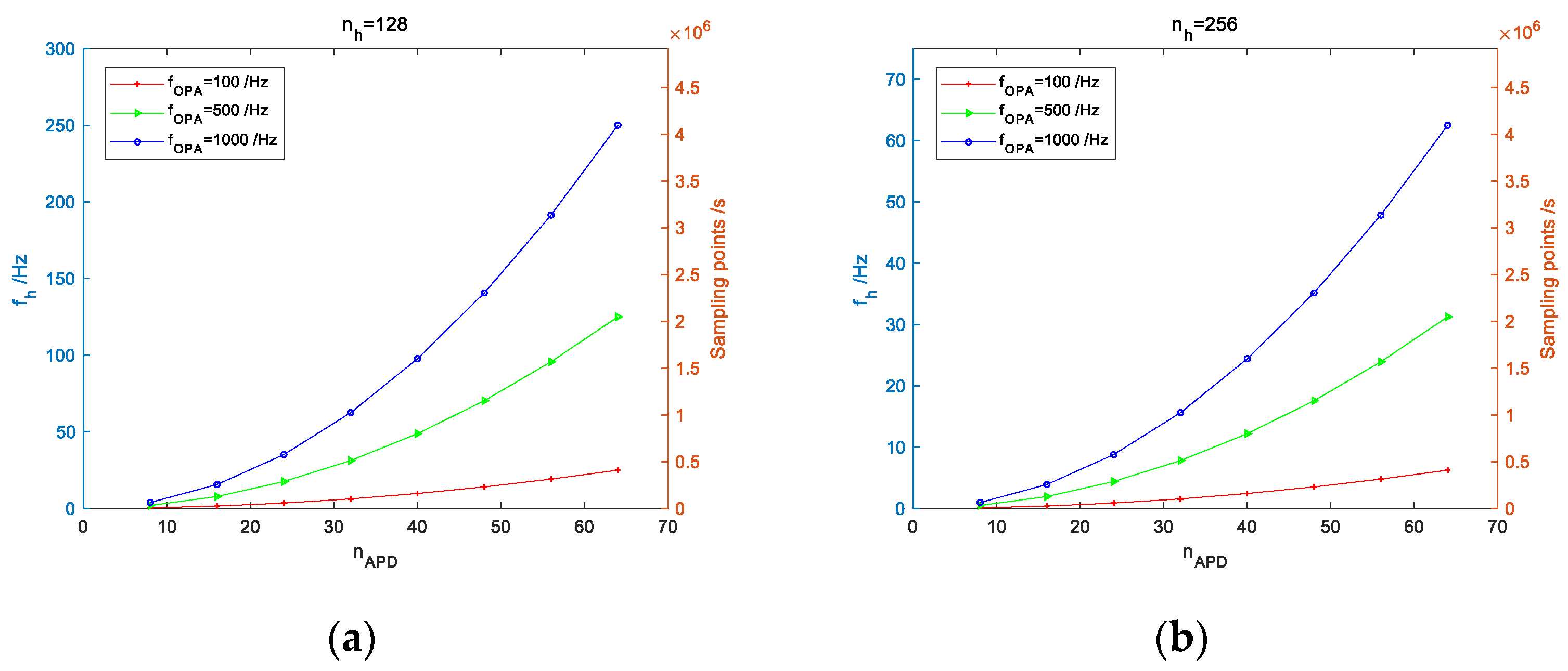
3.2.3. Number of Sampling Points

The number of sampling points for beam array scanning is determined by the times the sub-beam can scan within the corresponding pixel and the number of LM-APD array pixels, and is related to the instantaneous FOV angle of the pixel θ IFOV , the divergence angle of the sub-beam θ sub , and the smallest scanning angle θ scan _ min that can be realized by the optical phased array as shown in Equation (28):
r APD = n APD θ IFOV max ( θ sub , θ scan _ min ) 2
θ scan _ min is related to the number of phase modulation stages n bit of the optical phased array as Equation (29) shows:
2 π λ d OPA sin θ scan 2 π 2 n bit
thus
θ scan _ min = arcsin ( λ 2 n bit d OPA )
Equation (30) shows that both reducing the array element size of the optical phased array and increasing the number of phase modulation stages can achieve a higher scanning accuracy. Figure 13 shows the generation of a 5 × 5 beam array at a distance of 5 m using a liquid crystal modulator with a modulation of 8 bits and an array element size of 6.3 μm, combined with a laser with a wavelength of 532 nm and a divergence angle of about 2 mrad. The first row shows the distribution of the 5 × 5 beam array on the target plate at 5 m, and the second row shows a magnified view of the bright spot at the center. The minimum scale in the figure is 1 mm; it shows that the minimum scanning angle of the beam array at 5 m is about 2 mm, i.e., 0.4 mrad, and the minimum theoretical value is 0.33 mrad, so the theoretical analysis agrees well with the experimental values. In this case, the sub-beam divergence angle θ sub is larger than the minimum scanning angle θ scan _ min , and the maximum number of sampling points is decided by the maximum number of sampling points θ sub .
From Equations (29) and (30), the maximum number of sampling points is as shown in Equation (31):
r APD = n APD θ IFOV max [ θ sub , arcsin ( λ / n bit d OPA ) ] 2
The number of sampling points is determined by both θ sub and arcsin ( λ / n bit d OPA ) , i.e., max [ θ sub , arcsin ( λ / n bit d OPA ) ] .

3.2.4. Beam Energy Uniformity

The energy difference within the beam array is mainly due to the different energy distribution in each diffraction energy level when the beam is split. Figure 14 shows the energy distribution of four beams when the beam ratio is 4 × 4 and the deflection angle of the beam array is (0 mrad, 0 mrad) and (0 mrad, 5 mrad). It also shows that the scanning causes equal proportional attenuation of the energy of each sub-beam, but does not affect the uniformity.
The individual inconsistency within the sub-beam caused by beam splitting is as shown in Equation (32):
Δ P = 1 m M , 1 n N [ P g ( m , n ) P ¯ g ] M N
Δ P is less than 0.1% in most cases.

3.2.5. Energy Efficiency

The energy efficiency is the ratio of the sum of the energies of all the arrays in the beam array to the total energy of the laser beam incident in the optical phased array, and the energy efficiency will mainly affect the working distance of the 3D imaging system. It is shown in Equation (33):
η OPA = i = 1 m APD j = 1 n APD P sub ( i , j ) P in
The energy of the beam array is jointly affected by the beam generation and scanning, the multi-stage diffraction efficiency can be calculated cumulatively as shown in Equation (34):
η OPA = η r η g η s
where η r is the reflectance or transmittance of the optical phased array to the beam, which is an intrinsic parameter of the optical phased array device; η g is the change in energy efficiency caused by beam splitting, which can be obtained by the P E in Equation (13); and η s is the cumulative change in efficiency caused by the scanning angle in the x direction and the scanning angle in the y direction, as shown in Equation (35):
η s = [ sin π d OPA sin θ x / λ π d OPA sin θ x / λ ] 2 [ sin π d OPA sin θ y / λ π d OPA sin θ y / λ ] 2
Combining Equations (13) and (35), Equation (36) shows the energy efficiency:
η OPA = η r P E P in [ sin π d OPA sin θ x / λ π d OPA sin θ x / λ ] 2 [ sin π d OPA sin θ y / λ π d OPA sin θ y / λ ] 2
Equation (36) shows that using optical phased array modulator devices with higher reflectivity and optimization of the energy efficiency of beam splitting are two ways to improve the energy efficiency of the system with a fixed FOV. When η r = 0.8 , the beam arrays are 9 × 9 and 32 × 32 and the relationship between the energy efficiency of different wavelength lasers modulated by the optical phased array and the scanning angle and the array element size are as shown in Figure 15.
Figure 15a shows that the shorter the laser wavelength, the more the energy efficiency is affected by the scanning angle, and the maximum scanning angle required for beam array scanning is 2 θ r / n OPA . Figure 15b shows that there is little relationship between energy efficiency and array element size at array element sizes between 1 μm and 10 μm.

3.2.6. Imaging Frame Rate

Without considering the effects of laser re-frequency and LM-APD response time, the frame rate f h is related to the desired number of sampling points n h , the number of LM-APD array pixels n APD and the scanning frequency of the optical phased array f OPA as shown in Equation (37) demonstrates:
f h = n APD 2 n h 2 f OPA
Figure 16 shows the f h and the corresponding number of samples per second under different conditions.
Figure 16 shows that our method performs well in both imaging frame frequency and sampling points when the LM-APD array is larger than 32 × 32. Increasing the frequency of the optical phased array and the number of LM-APD pixels helps to improve the frame rate.

3.2.7. Phase Modulation Devices

The influence of the grating flap formed by the phase modulator device on the imaging is mainly analyzed. The grating flap is a superimposed interference enhancement of light waves that also occurs in specific directions in addition to the direction of the main flap, forming a grating flap, as shown in Equation (38):
2 π d OPA sin θ m λ Δ φ OPA = ± 2 m π
where θ m is the angle of the grating appearance. Typically, optical phased arrays only utilize the main flap at m = 0 , and when m 0 , the flap that appears at θ m is the grating flap. Equation (21) is a special form of Equation (38). The grating flap affects the energy efficiency of the beam array and also affects the energy distribution in the far field. Equation (39) shows the condition for the optical phased array scanning without a grating flap:
d OPA < λ 1 + | sin θ OPA |
The laser wavelength is shorter than the commonly used radar wavelength, and the center distance of the array elements of the liquid crystal phase modulator at this stage is large relative to the laser wavelength, which obviously cannot satisfy the requirements of Equation (39). The suppression of the grating flap is a major problem in the application of optical phased arrays, and it is difficult to eliminate it when an equally spaced optical phased array is used. Figure 17 shows the relative energy distribution in the far field obtained by simulation after deflecting the beam array by different angles, the multiple peaks in the center are the multiple sub-beams.
Figure 17 shows that when the scanning angle of the beam array is 10 mrad, 20 mrad, and 30 mrad, the grating flaps appear at −107 mrad and 127 mrad, −97 mrad and 137 mrad, and −87 mrad and 147 mrad, respectively. However, the method in this paper only needs to ensure that the grating flap at the high energy level does not appear in the FOV by using a finite receiving FOV matched to the beam array to receive the laser echo. The interference of the grating flap can be avoided by making the angle between the grating flap and the main flap larger than the receiving field of view angle, as shown in Equation (40):
| arcsin ( sin θ 0 ± m λ L / d OPA ) θ 0 | > θ R
The modulation parameters designed according to the requirements of Equation (40) are used for physical experiments at a distance of 5 m. The spot distribution obtained after adding an aperture diaphragm between the LCSLM and the target is shown in Figure 18a, and it can be seen that the influence of the grating flap has been mostly filtered out. Figure 18b shows the distribution of the beam array in the receiving optical system.
Although the interference of the grating on the beam array can be avoided, the loss of energy is unavoidable, but the energy utilization of the beam array in the APD duty cycle of 2/3 more than the floodlighting of about 30% [23], to a certain extent, can make up for the loss of energy.

4. Results

Using the reflective liquid crystal modulator as the phased array device and the LM-APD array as the receiver, Figure 19a shows the block diagram of the optical path of the designed experimental system, and Figure 19b shows the actual experimental system. The LCSLM is GCI-770402; the laser used in the experiment is Beamtech Optronics Co., Ltd. (Beijing, China) DAWA 200; we chose the laser at a 532 nm wavelength because it is visible and the optical path is easy to adjust. The laser at the transmitting end is incident on the liquid crystal modulator after passing through a 532 nm bandpass filter and attenuator, and a unit detector is placed near the beam expander mirror of the laser to receive the trigger as the timing start signal. The liquid crystal modulator loads the modulation phase, generates the beam array and controls the scanning angle. At the receiving end, the LM-APD array realizes the coaxial adjustment with the beam array through the three-way adjustment base. The laser echoes are received by the LM-APD array after the convergence of the receiving optical system, and the distance values corresponding to each pixel of the LM-APD array can be obtained by calculating the trigger time difference between the main waveform and the various echo signals. The 3D image can be obtained after processing. We used an oscilloscope to record the analog and digital signals output from the APDs, due to the limited number of channels of the oscilloscope (maximum 16 digital channels). The purpose of the experiment is to distinguish more details of the target in the parallel direction for a 4 × 4 LM-APD array by increasing its sampling points to 8 × 8, i.e., the resolution of 3D imaging is increased by a factor of 4 using the method of this paper.
Figure 20a shows the target which is a 32 cm × 32 cm white grid divided into 8 × 8 small grids, each of which is 4 cm × 4 cm in size, at a target distance of 20 m, with a wall 1 m behind the target. The received field of view of the system is 16 mrad, i.e., the instantaneous field of view of a single pixel at 20 m is 8 cm × 8 cm, i.e., one LM-APD pixel corresponds to 4 grids. From the calculation of the laser parameters, the minimum spot size of the sub-beam at 20 m is about 2.7 cm. Considering the adjustment error of the consistency of the optical axis of each sub-beam and the corresponding LM-APD pixel, four scans are performed in each field of view, i.e., the scanning angle between the two scans is slightly larger than the divergence angle of the sub-beam.
Figure 20b shows the distribution of the beam array at the target during the four scans; during the first scan, all the sub-beams of the beam array are at the lower-left position of the LM-APD pixel; during the second scan, all the sub-beams of the beam array are at the upper-left position of the LM-APD pixel, and the beam array irradiates to the wall behind the target because of the small hole at the upper-left corner; during the third scan, all the sub-beams of the beam array are at the lower-right position of the LM-APD pixel, similar to the second scan, and also irradiate to the wall behind the target; during the fourth scan, all the sub-beams of the beam array are at the lower-right position of the LM-APD pixel. In the third scan, the beam array sub-beams are all in the lower right corner of the LM-APD pixel, similar to the second scan, and also irradiate to the wall behind the target. In the fourth scan, the beam array sub-beams are all in the lower right corner of the LM-APD pixel. In this way, after four scans, four subdivisions of each pixel can be realized.
The median value was taken after excluding the larger error values after multiple imaging, and Figure 21 shows the results. Figure 21a shows the results obtained by direct flood illumination with a 4 × 4 LM-APD array, and Figure 21b,c show the 3D imaging results obtained after four scans using the method in this paper. Figure 21b,c show that the cardboard imaging result at 20 m has high resolution, but the distance error is large when imaging on the 21 m wall. There may be four main reasons for this: first, the timing stop signal error is more serious because the target is a diffuse reflecting plane with a lower echo signal-to-noise ratio. Second, the LM-APD array used in the experiment has a low duty cycle in the image sensing area, which causes the energy loss of the sub-beam echo and affects the range accuracy. Third, when the beam array is scanned to the wall, such as the second scan and third scan, the target will act as an aperture for the laser echo, with a certain degree of energy loss, which will make the distance value in the second scan and third scan large when using the frontier threshold method of identification. However, it can be seen that the distance values of each grid obtained using the beam array scanning method in this paper are, in general, consistent with the actual distance values of the grid of the target.

5. Discussion and Conclusions

Aiming at the problem that the small number of pixels in an LM-APD array affects the 3D imaging resolution at the present stage, we propose a method to improve the 3D imaging resolution by subdividing the pixel with a beam array based on optical phased array. First, the basic principle of the method is analyzed, and then a fast design method of cascade modulation is proposed according to the principle of optical phased array, which realizes the generation and scanning of the beam array at the same time with one phase modulation device. The relationship between the 3D imaging performance of the system and the main parameters is analyzed according to the actual parameters of the LM-APD array and the liquid crystal phase modulator, and the effects of typical parameters on the imaging performance are compared. Finally, 3D imaging experiments using the liquid crystal phase modulator and the LM-APD array are carried out to realize the scanning of the beam array in the far field and to verify the effectiveness of the method.
The results of analyses show that the method can effectively improve the 3D imaging resolution of the LM-APD array, and the simulation results prove that the method can improve the LM-APD 3D imaging resolution by at least 9 times. The multiplier of the improved resolution is equal to the ratio of the instantaneous FOV of pixel to the sub-beam divergence angle, and the scanning efficiency is improved by a multiplier equal to the number of the LM-APD pixels compared with single-point scanning, with better performance in terms of energy efficiency and beam uniformity. The sub-beam divergence angle under different deflection angles is analyzed, and the results prove that the greater the number of expansion cycles is, the smaller is the sub-beam divergence angle. The experimental results show that the resolution can be improved by a factor of 4 for imaging a target at 20 m.
The method only requires a single liquid crystal phase modulator to realize the beam array splitting and scanning, avoiding mechanical scanning, and has a good application prospect in the scenario of miniaturization of the 3D imaging volume and low power consumption requirements. The efficiency improvement compared with single-beam scanning of the unit detector is a multiple of the number of pixels n APD × n APD . It can also be flexibly configured according to the number of LM-APD array pixels and the receiving FOV of system, which also meets the requirements of miniaturization and low power consumption for UAVs, vehicles, and so on. When using the method in this paper, better imaging results are expected when a microlens array is added to the front of the LM-APD array. Limited by the experimental conditions, only the 3D imaging effect of increasing the resolution of the 4 × 4 LM-APD array by a factor of 4 was verified, but this method can also generate beam arrays with a larger number of beams, such as 64 × 64, to further improve the 3D imaging resolution of LM-APD arrays with a larger number of pixels. It should also be noted that the resolution enhancement effect and imaging frame rate are affected by the smaller deflection angle and the lower frame rate of the liquid crystal spatial light modulator when the liquid crystal modulator is used as an optical phased array, and the application of the method to the fiber-optic phased arrays should have a better resolution enhancement effect and imaging frame rate.

Author Contributions

Conceptualization, S.W. and L.L. (Lei Liu); methodology, K.-P.W. and G.-D.S.; software, L.Q.; validation, G.Y.; writing, L.L. (Ling Li); visualization, B.Z.; project administration, S.W. All authors have read and agreed to the published version of the manuscript.

Funding

This research received no external funding.

Institutional Review Board Statement

Not applicable.

Informed Consent Statement

Not applicable.

Data Availability Statement

Data are contained within the article.

Acknowledgments

We acknowledge the technical support received from Hua-Yan SUN and Hui-Chao GUO.

Conflicts of Interest

The authors declare no conflict of interest.

References

  1. Chang, L.; Liu, J.; Chen, Z.; Bai, J.; Shu, L. Stereo Vision-Based Relative Position and Attitude Estimation of Non-Cooperative Spacecraft. Aerospace 2021, 8, 230. [Google Scholar] [CrossRef]
  2. Haarlammert, T.; Kwiatkowski, A. Threat detection, identification and optical counter measures for space-based applications. In Proceedings of the High-Power Lasers and Technologies for Optical Countermeasures, Berlin, Germany, 5–8 September 2022; SPIE: Bellingham, WA, USA; Volume 12273, pp. 33–49. [Google Scholar]
  3. Sornsin, B.A.; Short, B.W. Global shutter solid state flash lidar for spacecraft navigation and docking applications. In Proceedings of the Laser Radar Technology and Applications XXIV, Baltimore, MD, USA, 14–18 April 2019; SPIE: Bellingham, WA, USA; Volume 11005, pp. 229–240. [Google Scholar]
  4. Pensado, E.A.; de Santos, L.M.G.; Sanjurjo-Rivo, M.; Jorge, H.G. Deep Learning Based Target Pose Estimation Using LiDAR Measurements in Active Debris Removal Operations. IEEE Trans. Aerosp. Electron. Syst. 2023, 59, 5658–5670. [Google Scholar] [CrossRef]
  5. Negri, R.B.; Prado, A.F.; Chagas, R.A.; de Moraes, R.V. Autonomous Rapid Exploration in Close-Proximity of an Asteroid. arXiv 2022, arXiv:2208.03378. [Google Scholar]
  6. Jin, C.F.; Wang, Y.; Cao, L.; Yu, M.; Liu, L.; Zhao, Y. Design of fiber-array image laser radar system. Opto-Electron. Eng. 2012, 39, 115. [Google Scholar]
  7. Zhou, G.; Zhou, X.; Yang, J.; Tao, Y.; Nong, X.; Baysal, O. Flash Lidar sensor using fiber-coupled APDs. IEEE Sens. J. 2015, 15, 4758–4768. [Google Scholar] [CrossRef]
  8. Ito, K.; Niclass, C.; Aoyagi, I.; Matsubara, H.; Soga, M.; Kato, S.; Maeda, M.; Kagami, M. System Design and Performance Characterization of a MEMS-Based Laser Scanning Time-of-Flight Sensor Based on a 256 × 64-pixel Single-Photon Imager. IEEE Photonics J. 2013, 5, 6800114. [Google Scholar] [CrossRef]
  9. Zhao, W.; Han, S. Cramer-Rao Lower Bound for the Range Accuracy of 3D Flash Imaging Lidar System. Trans. Beijing Inst. Technol. 2014, 34, 501–505. [Google Scholar]
  10. Amzajerdian, F.; Roback, V.E.; Bulyshev, A.E.; Brewster, P.F.; Carrion, W.A.; Pierrottet, D.F.; Hines, G.D.; Petway, L.B.; Barnes, B.W.; Noe, A.M. Imaging flash LIDAR for safe landing on solar system bodies and spacecraft rendezvous and docking. In Proceedings of the Laser Radar Technology and Applications XX; and Atmospheric Propagation XII, Baltimore, MD, USA, 20–24 April 2015; SPIE: Bellingham, WA, USA; Volume 9465, p. 946502. [Google Scholar]
  11. Heinrichs, R.; Aull, B.F.; Marino, R.M.; Fouche, D.G.; McIntosh, A.K.; Zayhowski, J.J.; Stephens, T.; O’Brien, M.E.; Albota, M.A. Three-dimensional laser radar with APD arrays. In Proceedings of the Laser Radar Technology and Applications VI, Orlando, FL, USA, 16–20 April 2001; SPIE: Bellingham, WA, USA; Volume 4377. [Google Scholar]
  12. Zhang, Y.; Cao, X.; Wu, L.; Zhang, S.; Zhao, Y. Experimental research on small scale risley prism scanning imaging laser radar system. Chin. J. Lasers 2013, 40, 0814001. [Google Scholar] [CrossRef]
  13. Sun, J. Three-Dimensional Laser Imaging System and Method Based on APD Array. China Patent CN105242281A, 13 January 2016. [Google Scholar]
  14. Li, Z.; Wu, E.; Pang, C.; Du, B.; Tao, Y.; Peng, H.; Zeng, H.; Wu, G. Multi-beam single-photon-counting three-dimensional imaging lidar. Opt. Express 2017, 25, 10189–10195. [Google Scholar] [CrossRef]
  15. Chen, Y.; He, Y.; Luo, Y. Pulsed Three-dimensional imaging lidar system based on Geiger-mode APD array. Chin. J. Lasers 2023, 50, 0210001. [Google Scholar]
  16. Kang, Y.; Xue, R.; Li, L. Coaxial scanning three-dimensional imaging based on SPAD array. Laser Optoelectron. Prog. 2021, 10, 1011024. [Google Scholar]
  17. Xie, S.; Zhao, Y.; Wang, Y.; Lv, H.; Jia, X. Microscanning laser imaging technology based on Geiger-mode APD array. Infrared Laser Eng. 2018, 12, 1206010. [Google Scholar]
  18. Wu, C.; Liu, C.; Han, X. Design of waveguide optical phased array ladar receiving system. Infrared Laser Eng. 2016, 10, 1030003. [Google Scholar]
  19. Yu, X.; Yao, Y.; Xu, Z. Laser imaging optical system design with a shared aperture employing APD array. Chin. Opt. 2016, 3, 349–356. [Google Scholar]
  20. Wang, S.; Huayan, S.; Guo, H. Application of dot-matrix illumination of liquid crystal phase space light modulator in 3D imaging of APD array. In Proceedings of the Nanophotonics Australasia 2017, Melbourne, Australia, 10–13 December 2017; SPIE: Bellingham, WA, USA; Volume 10456. [Google Scholar]
  21. Calò, G.; Bellanca, G.; Barbiroli, M.; Fuschini, F.; Serafino, G.; Bertozzi, D.; Tralli, V.; Petruzzelli, V. Design of reconfigurable on-chip wireless interconnections through Optical Phased Arrays. Opt. Express 2021, 29, 31212–31228. [Google Scholar] [CrossRef] [PubMed]
  22. Li, J.; Peng, Z.; Fu, Y. Diffraction transfer function and its calculation of classic diffraction formula. Opt. Commun. 2007, 280, 243–248. [Google Scholar] [CrossRef]
  23. Liu, B.; Zhao, J.; Sui, X.; Cao, C.; Yan, Z.; Wu, Z. Array beam laser three-dimensional imaging technology. Infrared Laser Eng. 2019, 48, 606001. [Google Scholar] [CrossRef]
Figure 1. Beam arrays are synthesized to improve resolution after scanning in the corresponding instantaneous field of view.
Photonics 10 01360 g001
Figure 2. Beam array scans from angle 1 to angle n in a 2 × 2 image element simultaneously.
Photonics 10 01360 g002
Figure 3. Schematic structure of a Dammann grating combined with a liquid crystal spatial light modulator to realize the method.
Photonics 10 01360 g003
Figure 4. Side view of the system for beam array scanning to improve resolution.
Photonics 10 01360 g004
Figure 5. Schematic diagram of the beam array control method: (a) sub-aperture method; (b) cascade modulation method.
Photonics 10 01360 g005
Figure 6. Schematic diagram of the wavefront tilt that deflects the direction of beam propagation.
Photonics 10 01360 g006
Figure 7. Beam array distribution at 10 m: (a) x = −1.56 mrad, y = 1.56 mrad; (b) x = 0 mrad, y = 1.56 mrad; (c) x = 1.56 mrad, y = 1.56 mrad; (d) x = −1.56 mrad, y = 0 mrad; (e) x = 0 mrad, y = 0 mrad; (f) x = 1.56 mrad, y = 0 mrad; (g) x = −1.56 mrad, y = −1.56 mrad; (h) x = 0 mrad, y = −1.56 mrad; (i) x = 1.56 mrad, y = −1.56 mrad.
Photonics 10 01360 g007
Figure 8. Beam array distribution at 10 m with liquid crystal light modulator: (a) x = 0 mrad, y = 1.56 mrad; (b) x = 0 mrad, y = 0 mrad; (c) x = 0 mrad, y = −1.56 mrad; (d) x = −1.56 mrad, y = 0 mrad; (e) x = 1.56 mrad, y = 0 mrad.
Photonics 10 01360 g008
Figure 9. Distribution of beam arrays on different object surfaces: (a) satellite model; (b) cylinder; (c) battery plate; (d) battery plate with aluminum plate in front.
Photonics 10 01360 g009
Figure 10. Relationship between beam array limitations on system field-of-view angle and array element size.
Photonics 10 01360 g010
Figure 11. Relationship between sub-beam divergence angle and. optical phased array size.
Photonics 10 01360 g011
Figure 12. Sub-beam divergence angle vs. optical phased array size: (a) distribution of the beam array in the far field at a scanning angle of (0 mrad, 0 mrad); (b) distribution of the beam array in the far field at a scanning angle of (1.56 mrad, 0 mrad).
Photonics 10 01360 g012
Figure 13. Beam array on target plate at 5 m: (a) x = 0 mrad y = 0 mrad; (b) x = 0.2 mrad y = 0 mrad; (c) x = 0.4 mrad y = 0 mrad; (d) x = 0.6 mrad y = 0 mrad; (e) x = 0.8 mrad y = 0 mrad; (f) x = 1 mrad y = 0 mrad.
Photonics 10 01360 g013
Figure 14. Energy distribution of the beam array at different scanning angles: (a) deflection angle of (0 mrad, 0 mrad); (b) deflection angle (0 mrad, 5 mrad).
Photonics 10 01360 g014
Figure 15. Energy efficiency versus scanning angle and array element size for different beam splitting ratios of the beam array: (a) energy efficiency versus scanning angle; (b) energy efficiency versus array element size.
Photonics 10 01360 g015
Figure 16. Relationship between frame rate and number of sampling points and LM-APD pixels and optical phased array frequency: (a) nh = 128; (b) nh = 256.
Photonics 10 01360 g016
Figure 17. Relative light intensity distribution of the beam array in the far field.
Photonics 10 01360 g017
Figure 18. Distribution of beam arrays at 5 m: (a) far-field distribution of beam array spot after adding aperture; (b) distribution of beam arrays in the field of view of the receiving optical system.
Photonics 10 01360 g018
Figure 19. The transmitter and receiver of the 3D imaging system: (a) block diagram of the system optical path; (b) experimental system.
Photonics 10 01360 g019
Figure 20. Distribution of the beam array on the target during scanning: (a) target at 20 m; (b) distribution of the beam array at the target for 4 scans.
Photonics 10 01360 g020
Figure 21. Increasing the resolution of a 4 × 4 LM-APD array by a factor of 4: (a) results of a 4 × 4 LM-APD array; (b) beam array scanning LM-APD array 3D imaging side view; (c) beam array scanning LM-APD array 3D imaging top view.
Photonics 10 01360 g021
Disclaimer/Publisher’s Note: The statements, opinions and data contained in all publications are solely those of the individual author(s) and contributor(s) and not of MDPI and/or the editor(s). MDPI and/or the editor(s) disclaim responsibility for any injury to people or property resulting from any ideas, methods, instructions or products referred to in the content.

