The Proposal of a Photon–Photon Resonance Control Scheme by Using an Active MMI Laser Diode


Abstract
:1. Introduction
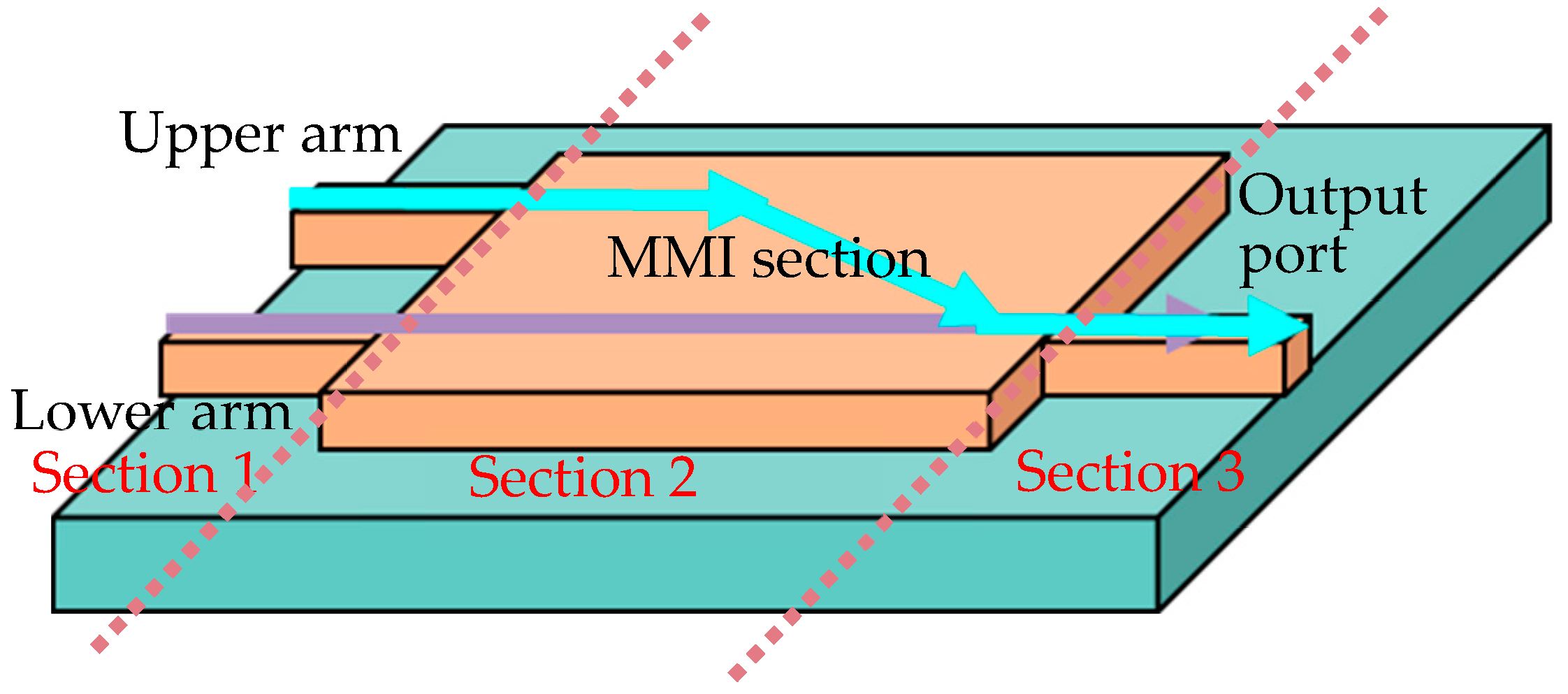
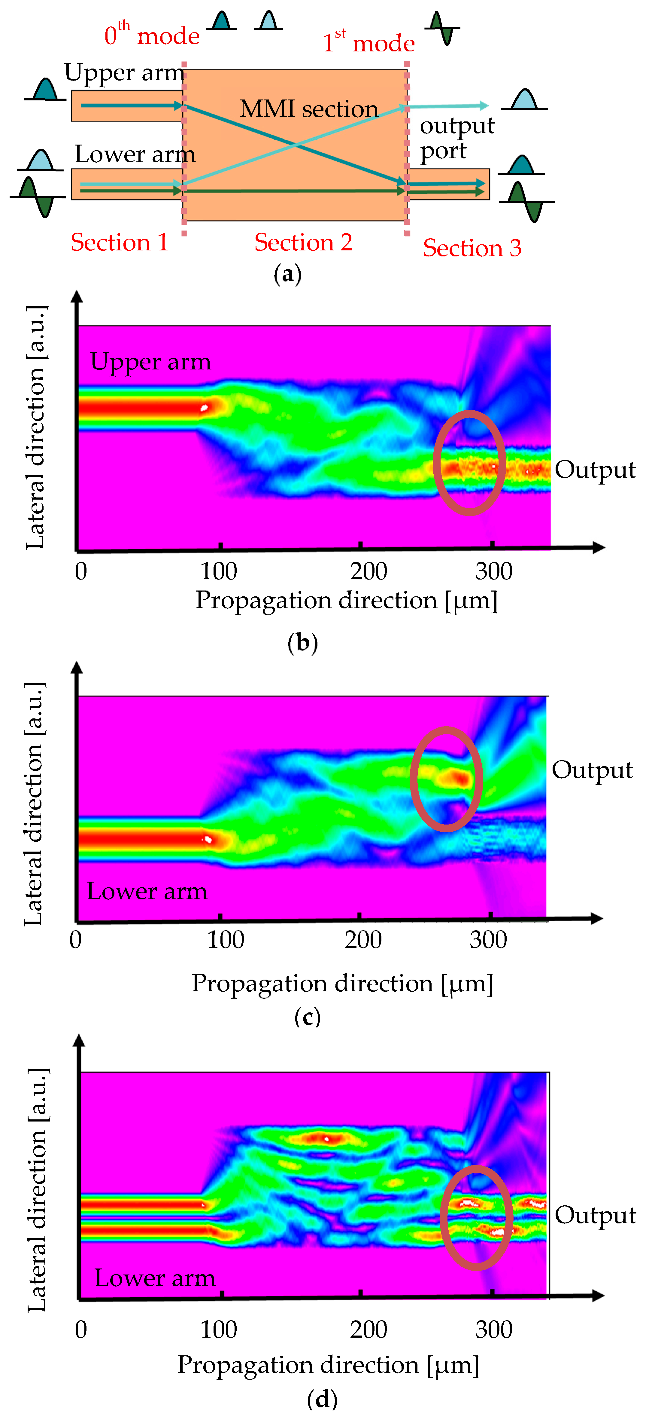
2. PPR Numerical Model in Proposed Active MMI LD
- (1)
- Equation (2): This equation is the derivative of the photon density for the sub-lasing mode, in addition to the one for the main lasing mode (Equation (1)).
- (2)
- As indicated, it involves a co-related term between the main and sub-lasing modes as a second term related to the coupling efficiency, . Note that, in Equation (1), this co-related term is neglected as the main lasing mode is strongly associated, rather than a sub-mode laser, in a laser cavity. Equation (3): This equation considers that this phase term relates to the co-relation in longitudinal mode.
- (3)
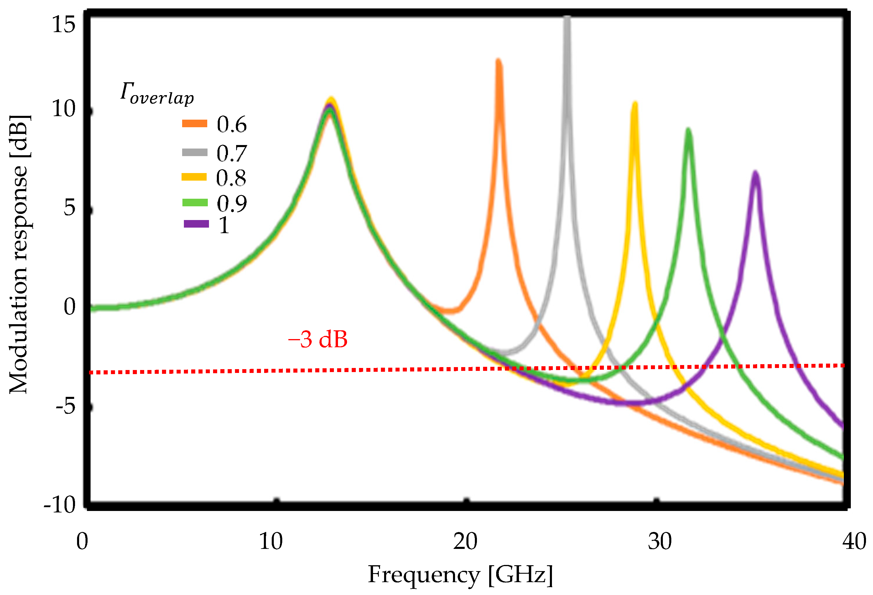
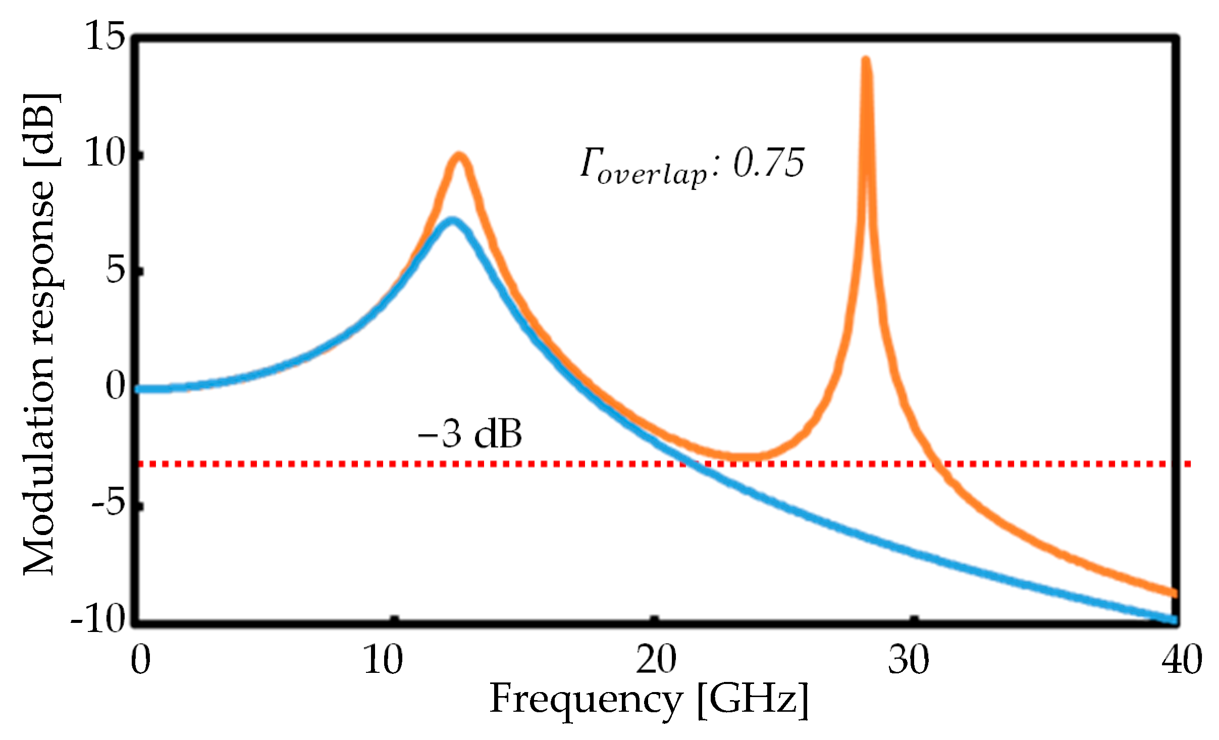
- To ensure that corresponds to the coupling efficiency between the main and sub-lasing modes, we introduce a coupling ratio in [27], which satisfies . is defined as the optical profile overlap of the lateral mode between the two lasing modes. In this situation, the coupling efficiency in the active MMI LD is:
- (4)
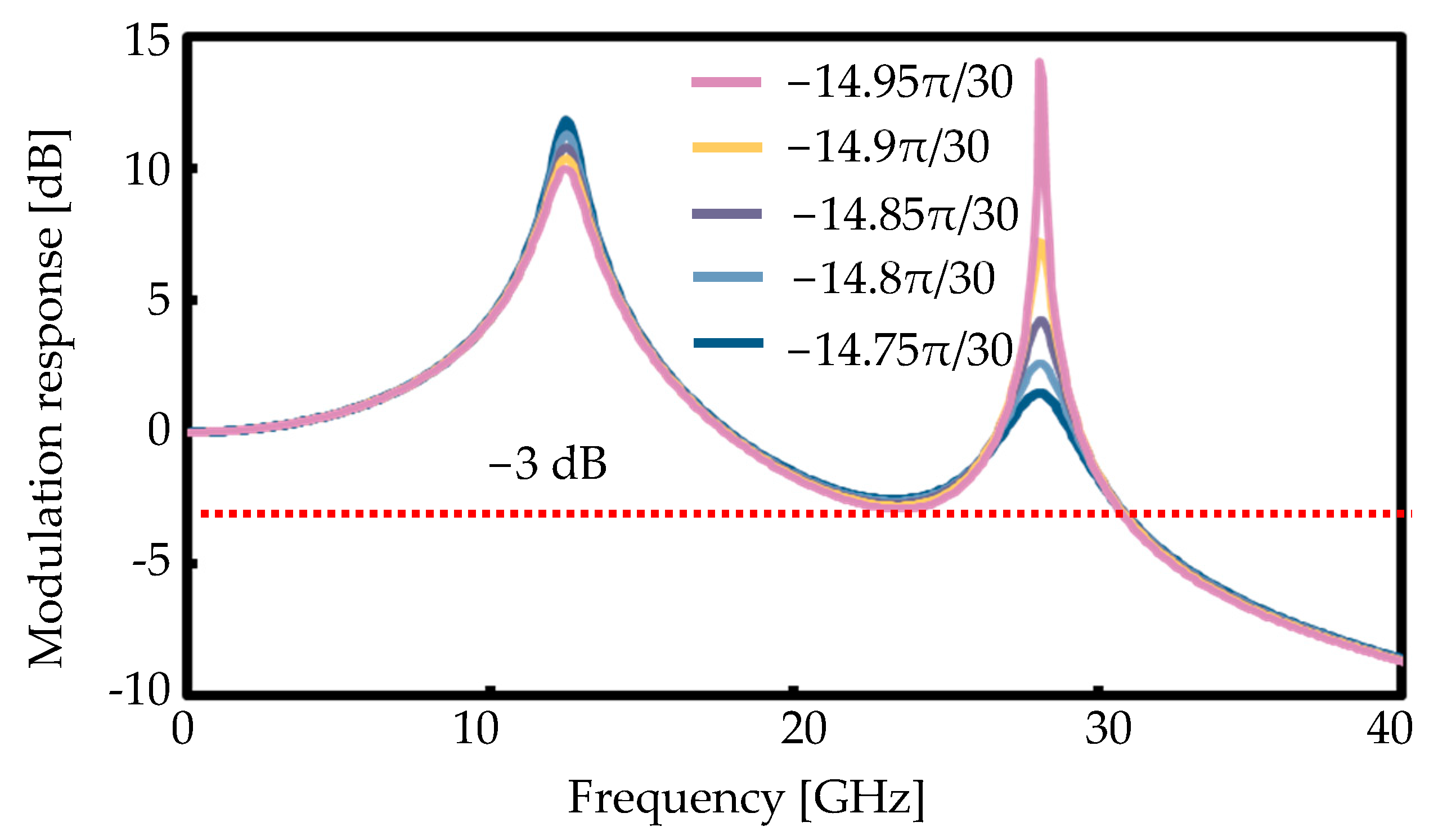
- affects PPR phenomena directly. The coupling efficiency is defined as the propagation of two lasers along the entire cavity to couple. The two lasing modes in the active MMI LD are not always present together, as visible in Section 1. As the 1 × N active MMI configuration may offer the possibility to control itself, we verify the effect of in the following.
3. Active MMI Configuration for the Control of PPR and Discussion
4. Discussion
5. Conclusions
Author Contributions
Funding
Institutional Review Board Statement
Informed Consent Statement
Data Availability Statement
Conflicts of Interest
Appendix A
References
- Rumley, S.; Bahadori, M.; Polster, R.; Hammond, S.D.; Calhoun, D.M.; Wen, K.; Rodrigues, A.; Bergman, K. Optical interconnects for extreme scale computing systems. Parallel Comput. 2017, 64, 65–80. [Google Scholar] [CrossRef]
- Faanes, G.; Bataineh, A.; Roweth, D.; Court, T.; Froese, E.; Alverson, B.; Johnson, T.; Kopnick, J.; Higgins, M.; Reinhard, J. Cray Cascade: A scalable HPC system based on a Dragonfly network. In Proceedings of the SC’12: Proceedings of the International Conference on High Performance Computing, Networking, Storage and Analysis, Salt Lake City, UT, USA, 10–16 November 2012; pp. 1–9. [Google Scholar]
- Ajima, Y.; Kawashima, T.; Okamoto, T.; Shida, N.; Hirai, K.; Shimizu, T.; Hiramoto, S.; Ikeda, Y.; Yoshikawa, T.; Uchida, K.; et al. The Tofu Interconnect D. In Proceedings of the 2018 IEEE International Conference on Cluster Computing (CLUSTER), Belfast, UK, 10–13 September 2018; pp. 646–654. [Google Scholar]
- Alverson, R.; Roweth, D.; Kaplan, L. The Gemini System Interconnect. In Proceedings of the 2010 18th IEEE Symposium on High Performance Interconnects, Mountain View, CA, USA, 18–20 August 2010; pp. 83–87. [Google Scholar]
- Kilper, D.; Bergman, K.; Chan, V.W.; Monga, I.; Porter, G.; Rauschenbach, K. Optical Networks Come of Age. Opt. Photonics News 2014, 25, 50–57. [Google Scholar] [CrossRef]
- Matsui, Y. Direct modulated laser technology: Past, present, and future. In Datacenter Connectivity Technologies: Principles and Practice; River Publisher: Gistrup, Demark, 2018; pp. 87–90. [Google Scholar]
- Radziunas, M.; Glitzky, A.; Bandelow, U.; Wolfrum, M.; Troppenz, U.; Kreissl, J.; Rehbein, W. Improving the modulation bandwidth in semiconductor lasers by passive feedback. IEEE J. Sel. Top. Quantum Electron. 2007, 13, 136–142. [Google Scholar] [CrossRef]
- Vallone, M.; Bardella, P.; Montrosset, I. Enhanced modulation bandwidth in complex cavity injection grating lasers. IEEE J. Quantum Electron. 2011, 47, 1269–1276. [Google Scholar] [CrossRef]
- Nowell, M.C.; Carroll, J.E.; Plumb, R.G.S.; Marcenac, D.D.; Robertson, M.J.; Wickes, H.; Zhang, L.M. Low-chirp and enhanced-resonant frequency by direct push-pull modulation of DFB lasers. IEEE J. Sel. Top. Quant. Electron. 1995, 1, 433–441. [Google Scholar] [CrossRef]
- Kaiser, W.; Bach, L.; Reithmaier, J.P.; Forchel, A. High-speed coupled-cavity injection grating lasers with tailored modulation transfer functions. IEEE Photonics Technol. Lett. 2004, 16, 1997–1999. [Google Scholar] [CrossRef]
- Gerschütz, F.; Fischer, M.; Koeth, J.; Krestnikov, I.; Kovsh, A.; Schilling, C.; Kaiser, W.; Höfling, S.; Forchel, A. 1.3 µm Quantum Dot Laser in coupled-cavity-injection-grating design with bandwidth of 20 GHz under direct modulation. Opt. Express 2008, 16, 5596–5601. [Google Scholar] [CrossRef]
- Bach, L.; Kaiser, W.; Reithmaier, J.; Forchel, A.; Gioannini, M.; Feies, V.; Montrosset, I. 22-GHz modulation bandwidth of long cavity DBR laser by using a weakly laterally coupled grating fabricated by focused ion beam lithography. IEEE Photonics Technol. Lett. 2004, 16, 18–20. [Google Scholar] [CrossRef]
- de Valicourt, G.; Levaufre, G.; Pointurier, Y.; Le Liepvre, A.; Antona, J.C.; Jany, C.; Accard, A.; Lelarge, F.; Make, D.; Duan, G.H. Direct modulation of hybrid-integrated InP/Si transmitters for short and long reach access network. J. Light. Technol. 2015, 33, 1608–1616. [Google Scholar] [CrossRef]
- Troppenz, U.; Kreissl, J.; Moehrle, M.; Bornholdt, C.; Rehbein, W.; Sartorius, B.; Woods, I.; Schell, M. 40 Gbit/s directly modulated lasers: Physics and application. In Proceedings of the Novel In-Plane Semiconductor Lasers, San Francisco, CA, USA, 25–28 January 2011; Volume 7953, pp. 98–107. [Google Scholar]
- Hong, B.; Kitano, T.; Mori, T.; Jiang, H.; Hamamoto, K. Bandwidth enhancement scheme demonstration on direct modulation active-MMI laser diode using multiple photon photon resonance. Appl. Phys. Lett. 2017, 111, 221105. [Google Scholar] [CrossRef]
- Reithmaier, J.P.; Kaiser, W.; Bach, L.; Forchel, A.; Feies, V.; Gioannini, M.; Montrosset, I.; Berg, T.W.; Tromborg, B. Modulation speed enhancement by coupling to higher order resonances: A road towards 40 GHz bandwidth lasers on InP. In Proceedings of the International Conference on Indium Phosphide and Related Materials, Glasgow, UK, 8–12 May 2005; pp. 118–123. [Google Scholar]
- Dumitrescu, M.; Telkkälä, J.; Karinen, J.; Viheriälä, J.; Laakso, A.; Afzal, S.; Reithmaier, J.P.; Kamp, M.; Melanen, P.; Uusimaa, P.; et al. High-speed directly-modulated lasers with photon-photon resonance. In Proceedings of the IPRM 2011–23rd International Conference on Indium Phosphide and Related Materials, Berlin, Germany, 22–26 May 2011; pp. 1–4. [Google Scholar]
- Hong, B.; Mori, T.; Jiang, H.; Hamamoto, K. Mode selective active multimode interferometer laser diode with over 40 GHz direct modulation bandwidth. In Proceedings of the Optical Fiber Communication Conference, San Diego, CA, USA, 11–15 March 2018; p. Th3B-4. [Google Scholar]
- Murakami, S.; Hong, B.; Jiang, H.; Hamamoto, K. Observation of 60 GHz and 20 GHz Multiple Photon-Photon Resonances Using Active Multimode Interferometer Laser Diodes. In Proceedings of the 2019 24th Microoptics Conference (MOC), Toyama, Japan, 17–20 November 2019; pp. 304–305. [Google Scholar]
- Bardella, P.; Chow, W.W.; Montrosset, I. Design and analysis of enhanced modulation response in integrated coupled cavities DBR lasers using photon-photon resonance. Photonics 2016, 3, 4. [Google Scholar] [CrossRef]
- Bach, L.; Kaiser, W.; Reithmaier, J.P.; Forchel, A.; Berg, T.W.; Tromborg, B. Enhanced direct-modulated bandwidth of 37 GHz by a multi-section laser with a coupled-cavity-injection-grating design. Electron. Lett. 2003, 39, 1592–1593. [Google Scholar] [CrossRef]
- Matsui, Y.; Schatz, R.; Che, D.; Khan, F.; Kwakernaak, M.; Sudo, T. Low-chirp isolator-free 65-GHz-bandwidth directly modulated lasers. Nat. Photonics 2021, 15, 59–63. [Google Scholar] [CrossRef]
- Rajeswari, G.V.; Moehrle, M.; Ehrensack, F.; Troppenz, U.; Sigmund, A.; Schell, M. Novel > 57 GHz bandwidth O-band InGaAlAs MQW RW DFB. In Proceedings of the Novel In-Plane Semi Lasers XXII, San Francisco, CA, USA, 31 January–2 February 2023; Volume 3, pp. 34–39. [Google Scholar]
- Yamaoka, S.; Diamantopoulos, N.P.; Nishi, H.; Nakao, R.; Fujii, T.; Takeda, K.; Hiraki, T.; Tsurugaya, T.; Kanazawa, S.; Tanobe, H.; et al. Directly modulated membrane lasers with 108 GHz bandwidth on a high-thermal-conductivity silicon carbide substrate. Nat. Photonics 2021, 15, 28–35. [Google Scholar] [CrossRef]
- Ahmed, M.; Bakry, A.; Alghamdi, M.S.; Dalir, H.; Koyama, F. Enhancing the modulation bandwidth of VCSELs to the millimeter-waveband using strong transverse slow-light feedback. Opt. Express 2015, 23, 15365–15371. [Google Scholar] [CrossRef]
- Hamamoto, K.; Jiang, H. Active MMI devices: Concept, proof, and recent progress. J. Phys. D Appl. Phys. 2015, 48, 383001. [Google Scholar] [CrossRef]
- Jiang, H.; Bastawrous, H.A.; Hagio, T.; Matsuo, S.; Hamamoto, K. Low hysteresis threshold current (39 mA) active multimode-interferometer. IEEE J. Sel. Top. Quantum Electron. 2011, 17, 1258–1263. [Google Scholar] [CrossRef]
- Pikovsky, A.; Rosenblum, M.; Kurths, J. Synchronization, A Universal Concept in Nonlinear Sciences, 1st ed.; Cambridge University Press: New York, NY, USA, 2001; pp. 53–56. [Google Scholar]
- Murakami, A.; Kawashima, K.; Atsuki, K. Cavity resonance shift and bandwidth enhancement in semiconductor lasers with strong light injection. IEEE J. Quantum Electron. 2003, 39, 1196–1204. [Google Scholar] [CrossRef]
- Lang, R. Injection locking properties of a semiconductor laser. IEEE J. Quantum Electron. 1982, 18, 976–983. [Google Scholar] [CrossRef]
- Lau, E.K.; Sung, H.K.; Wu, M.C. Frequency response enhancement of optical injection-locked lasers. IEEE J. Quantum Electron. 2007, 44, 90–99. [Google Scholar] [CrossRef]
- Lau, E.K.; Wong, L.J.; Wu, M.C. Enhanced modulation characteristics of optical injection-locked lasers: A tutorial. IEEE J. Sel. Top. Quantum Electron. 2009, 15, 618–633. [Google Scholar] [CrossRef]
- Lau, E.K.; Sung, H.K.; Wu, M.C. Scaling of resonance frequency for strong injection-locked lasers. Opt. Lett. 2007, 32, 3373–3375. [Google Scholar] [CrossRef] [PubMed]
- Simpson, T.B.; Liu, J.M.; Gavrielides, A. Bandwidth enhancement and broadband noise reduction in injection-locked semiconductor lasers. IEEE Photonics Technol. Lett. 1995, 7, 709–711. [Google Scholar] [CrossRef]
- Mogensen, F.; Olesen, H.; Jacobsen, G. Locking conditions and stability properties for a semiconductor laser with external light injection. IEEE J. Quantum Electron. 1985, 21, 784–793. [Google Scholar] [CrossRef]
- Liu, Z.; Slavík, R. Optical injection locking: From principle to applications. J. Light. Technol. 2020, 38, 43–59. [Google Scholar] [CrossRef]
- Henry, C.; Olsson, N.; Dutta, N. Locking range and stability of injection locked 1.54 µm InGaAsP semiconductor lasers. IEEE J. Quantum Electron. 1985, 21, 1152–1156. [Google Scholar] [CrossRef]
- Xiao, H.; Shoda, K.; Koudu, K.; Jiang, H.; Hamamoto, K. Affection analysis of frequency response with photon-photon-resonance (PPR) to directly modulated 40 Gbps signal. In Proceedings of the 2021 26th Microoptics Conference (MOC), Hamamatsu, Japan, 26–29 September 2021; pp. 1–2. [Google Scholar]
- Siegman, A.E. LASERS, 1st ed.; University Science Books US: Sausalito, CA, USA, 1986; pp. 187–211. [Google Scholar]
- Coldren, L.A.; Corzine, S.W.; Mashanovitch, M.L. Diode Lasers and Photonic Integrated Circuits, 2nd ed.; John Wiley & Sons: Hoboken, NJ, USA, 2012; pp. 260–279. [Google Scholar]
- Suematsu, Y.; Adams, A.R. Handbook of Semiconductor Lasers and Photonic Integrated Circuits, 1st ed.; Ohmsha Press: Tokyo, Japan, 1994; pp. 262–273. [Google Scholar]
- Manning, J.; Olshansky, R.; Su, C. The carrier-induced index change in AlGaAs and 1.3 μm InGaAsP diode lasers. IEEE J. Quantum Electron. 1983, QE-19, 1525–1530. [Google Scholar] [CrossRef]
- Bennett, B.R.; Soref, R.A.; Del Alamo, J.A. Carrier-induced change in refractive index of InP, GaAs and InGaAsP. IEEE J. Quantum Electron. 1990, 26, 113–122. [Google Scholar] [CrossRef]
- Zang, Z.; Mukai, K.; Navaretti, P.; Duelk, M.; Velez, C.; Hamamoto, K. Thermal resistance reduction in high power superluminescent diodes by using active multi-mode interferometer. Appl. Phys. Lett. 2012, 100, 031108. [Google Scholar] [CrossRef]
- Varshni, Y.P. Comparative study of potential energy functions for diatomic molecules. Rev. Mod. Phys. 1957, 29, 664–682. [Google Scholar] [CrossRef]
- Varshni, Y.P. Temperature dependence of the energy gap in semiconductors. Physica 1967, 34, 149–154. [Google Scholar] [CrossRef]
- Gupta, V.P.; Ravindra, N.M. Comments on the moss formula. Phys Status Solidi (b) 1980, 100, 715–719. [Google Scholar] [CrossRef]


| Symbol | Value | Unit |
|---|---|---|
| 7888 | 1/s | |
| 1972 | 1/s | |
| 2.5 × 10⁹ | # | |
| α | 5 | - |
| 2 × | 1/s | |
| 7.5 × 10¹⁷ | 1/s | |
| 8.3 × 10⁻⁹ | s | |
| 2.8 × 10⁻¹² | s | |
| 7.34 × 10⁻¹² | s | |
| L | 360 | µm |
| 125.7 | 1/ns |
| Symbol | Value |
|---|---|
Disclaimer/Publisher’s Note: The statements, opinions and data contained in all publications are solely those of the individual author(s) and contributor(s) and not of MDPI and/or the editor(s). MDPI and/or the editor(s) disclaim responsibility for any injury to people or property resulting from any ideas, methods, instructions or products referred to in the content. |
© 2023 by the authors. Licensee MDPI, Basel, Switzerland. This article is an open access article distributed under the terms and conditions of the Creative Commons Attribution (CC BY) license (https://creativecommons.org/licenses/by/4.0/).
Share and Cite
Xiao, H.; Kawano, Y.; Jiang, H.; Hamamoto, K. The Proposal of a Photon–Photon Resonance Control Scheme by Using an Active MMI Laser Diode. Photonics 2023, 10, 1298. https://doi.org/10.3390/photonics10121298
Xiao H, Kawano Y, Jiang H, Hamamoto K. The Proposal of a Photon–Photon Resonance Control Scheme by Using an Active MMI Laser Diode. Photonics. 2023; 10(12):1298. https://doi.org/10.3390/photonics10121298
Chicago/Turabian StyleXiao, He, Yudai Kawano, Haisong Jiang, and Kiichi Hamamoto. 2023. "The Proposal of a Photon–Photon Resonance Control Scheme by Using an Active MMI Laser Diode" Photonics 10, no. 12: 1298. https://doi.org/10.3390/photonics10121298
APA StyleXiao, H., Kawano, Y., Jiang, H., & Hamamoto, K. (2023). The Proposal of a Photon–Photon Resonance Control Scheme by Using an Active MMI Laser Diode. Photonics, 10(12), 1298. https://doi.org/10.3390/photonics10121298