Article

Interface Engineering and Electron-Hole Wave Function Overlap of InAs/AlSb Superlattice Infrared Detectors

1
School of Opto−Electronic Engineering, Changchun University of Science and Technology, Changchun 130022, China
2
School of Instrument Science and Opto-Electronics Engineering, Beijing Information Science and Technology University, Beijing 100192, China
3
School of Engineering, RMIT University, Melbourne 3000, Australia
*
Authors to whom correspondence should be addressed.
Photonics 2023, 10(11), 1268; https://doi.org/10.3390/photonics10111268
Submission received: 23 September 2023 / Revised: 7 November 2023 / Accepted: 14 November 2023 / Published: 16 November 2023
(This article belongs to the Special Issue Advanced Infrared Technology and Applications)

Abstract

:
InAs/AlSb is a material system that can be used as a low-noise avalanche detector and operates in the short-wave infrared band. The interface parameters determine the wave function overlap (WFO). Maximizing the WFO of InAs/AlSb superlattices improves the quantum efficiency (QE) of infrared avalanche photodetectors (APDs). However, this remains a huge challenge. Here, the 8-band k·p perturbation method based on Bloch wave envelope function approximation was used to calculate the energy level structure of InAs/AlSb superlattices. The results indicate that the WFO is enhanced with increasing InSb interface thickness or when the InSb (or AlAs) interface is far from the intersection of InAs and AlSb. As the AlAs interface thickness increases, the WFO enhances and then reduces. The maximum increase in WFO is 15.7%, 93%, and 156.8%, respectively, with three different models. Based on the stress equilibrium condition, we consider the interface engineering scheme proposed for enhancing WFO with an increase of 16%, 114%, and 159.5%, respectively. Moreover, the absorption wavelength shift is less than ±0.1 μm. Therefore, the interface layer thickness and position can be designed to enhance the WFO without sacrificing other properties, thereby improving the QE of the device. It provides a new idea for the material epitaxy of APDs.

1. Introduction

APDs in the short-wavelength infrared (SWIR) band (1~3 μm) are often used to detect weak signals reflected by distant objects because APDs have the advantage of a gain mechanism and high sensitivity. It is widely used in laser radar, gas sensing, astronomy, and 3D mapping. However, SWIR APDs still face the challenge of a high gain and low noise.
The mature materials of SWIR APDs include Si, HgCdTe (MCT), InGaAs, and AlInAsSb quaternary alloys. Bérard studied the principle of noise generated with Si avalanche photodiode structures. The excess noise factor of the front illuminated N-type and P-type structures is strongly dependent on wavelength, while the back illuminated structure is beneficial for reducing excess noise [1]. However, the absorption cutoff wavelength of Si APD is limited to 1 μm, which makes the detection range narrow. MCT can achieve near-constant exponential gain and low excess noise [2] by varying the Cd component to cover the short-wave range. It has the disadvantages of difficult epitaxy, complex back-end technology, and being expensive and toxic. The APD based on InGaAs material shows high performance in the wavelength range of 0.9~1.6 μm, and the use of InGaAsP to make the separate absorption, grading, charge, and multiplication (SAGCM) structure greatly reduces the device’s dark current and excessive noise factor [3]. When the cut-off wavelength exceeds 1.7 μm, the performance of APD rapidly decreases due to mismatch-induced defects. The antimonide-based AlInAsSb can flexibly adjust the heterostructural bandgap, matching the substrate lattice of InP [4], InAs [5], and GaSb [6]. Varying the aluminum content tuned the wavelength from 5 μm (0% aluminum) to 1.05 μm (72% aluminum). The Ohio State University reported in 2021 that Al0.79InAsSb APD grown on an InP substrate has a k value of 0.018, a dark current density of 82 μA/cm2, and a gain of 15 at room temperature [7]. The Microelectronics Research Center at the University of Texas reported a SAGCM APD based on the bulk material AlInAsSb, with a detection wavelength extended to 2 μm [8]. The device has a gain of 100 at room temperature and is exhibited very low over noise, with a k factor of approximately 0.01. In 2022, the unit also reported the SACM APD structure with an optical cutoff wavelength of 3 μm, which achieved low-light signal detection near mid-wave infrared at an operating temperature of 240 K [9]. Further, in 2023, the laboratory adopted a four-element alloy with an Al group of 0.05 as the detection material, with an external quantum efficiency of 24% (0.58 A/W) at 100 K and 3 μm [10]. The AlInAsSb compounds have great potential as candidate materials in the field of infrared APDs [11].
The InAs/AlSb superlattices of AlSb, InAs, and other binary compounds are successively epitaxial with molecular beam epitaxy (MBE) via the migration-enhanced method so that the AlInAsSb quaternary alloy can epitaxially contain high-quality materials in the miscible gap. InAs/AlSb superlattices can significantly reduce generation recombination (GR) dark current and band-to-band tunneling [12]. InAs/AlSb can design APDs with a wide wavelength range by adjusting the proportion of Al components. In addition, due to the slight valence band offset of different Al components [13], the SAGCM-typed APD has the advantages of low dark current, high gain, and extremely low noise [14]. The QE of SAGCM devices needs to be further enhanced to improve the conversion efficiency of APDs. At present, it mainly includes two methods: One is to increase the thickness of the material, but this would lead to high noise. The second is to enhance the WFO of the material. However, the electron-hole overlap of the InAs/AlSb superlattice exists only at the interface, and the electron-hole WFO of the superlattice is weak and quantum inefficient [15]. Therefore, the amount of electron-hole WFO in the InAs/AlSb superlattice urgently needs to be enhanced.
In previous studies, there were numerous ways to enhance QE by strengthening the electron-hole WFO of superlattices. For example, the GaSb layer is introduced into InAs/AlSb to form an “InAs/GaSb/AlSb/GaSb” M structure superlattice, and the electron-hole WFO is enhanced [16]. But hampered by the reduced electron mobility and additional interfaces, their QE is decreased. Wu et al. promoted As-Sb exchange at the interface by changing the growth temperature of InAs/AlSb superlattices, which formed a special band structure that can drive electrons and holes to the interface between InAs and AlSb, thereby improving the WFO of InAs/AlSb superlattices [17]. To obtain the optimal WFO, by applying a certain external voltage to the detector, the QE can be increased from 34% to 51% [18]. However, the working wavelength drift is affected by the existence of the Stark effect. Furthermore, there is a lattice mismatch between InAs and AlSb, and the performance of InAs/AlSb superlattices is affected by the critical thickness of strain equilibrium. Therefore, the WFO enhancement of superlattice without changing operating conditions and sacrificing growth quality remains a huge challenge. There have been relevant experiments proving that the introduction of AlAs [17] or InSb [19] interface layers in InAs/AlSb type-II superlattices enhances the electron-hole WFO.
Further, we introduced the InSb and AlAs interface layers in InAs/AlSb to address the above challenge. First, we study the relationship between the position of the interfacial layer in the electron-hole well and the WFO. Then, the interface engineering is established to balance the InAs/AlSb superlattice stress. Subsequently, the theoretical maximum value of WFO was sought by designing the layer thickness relationship between InSb and AlAs interfaces. Finally, the optimization results show that the WFO has been enhanced by at least 14%, and the wavelength drift range is as low as about 0.1 μm.

2. Theoretical Model

The k·p Hamiltonian is obtained using the Schrödinger equation of an electron. The Bloch wave function ψ n k ( r ) = e i k r u n k ( r ) is substituted into the Schrodinger equation and rewritten as the following equation:
H u n k ( r ) = E n ( k ) u n k ( r )
where H is the Kane Hamiltonian and u n k ( r ) is a periodic function. Here, we use 8-band coupled Hamiltonians, including the potential energy matrix, motion energy matrix, spin–orbit interaction matrix, and strain matrix, which are used to solve the conduction band, as well as the heavy hole band, light hole band, and spin–orbit splitting band. Each band has dual-spin degeneracy. The 8 × 8 Luttinger–Kohn (LK) Hamiltonian consists of the basic functions corresponding to the 8-band, which can be decoupled into a diagonal matrix:
H 8 × 8 LK = H 4 × 4 U 0 0 H 4 × 4 L
The original effective mass mc parameter in the 8-band model mainly describes the characteristic energy dispersion curve, and the electronic effective mass is corrected according to the experimental values as follows:
m 0 m c = m 0 m c E p ( E g + 2 Δ s o / 3 ) E g ( E g + Δ s o )
where Ep is the optical matrix parameter, Eg is the material bandgap, and Δ s o is spin–orbit splitting energy. Due to the coupling between the conduction band and valence band, the Luttinger parameter γ 1 L , γ 2 L , γ 3 L also needs to be modified:
γ 1 = γ 1 L E p ( 3 E g + Δ s o ) γ 2 = γ 2 L E p 2 * ( 3 E g + Δ s o ) γ 3 = γ 3 L E p 2 * ( 3 E g + Δ s o )
The initial parameters and corrected parameters are included in Table 1. It is shown in Ref. [20] that the corrected parameters are within the error range.
We use the Periodic Boundary Condition (PBC) method to solve the 8-band model. The periodic thickness of the superlattice is set to be L. Here, z represents the growth direction of the superlattice, and the wave function satisfies the periodic condition:
f m ( i ) ( k t , z + L ) = f m ( i ) ( k t , z )
where kt is the transverse wave number, and it describes the direction of the band structure in the transverse plane. The wave function is periodically repeated without any phase change. Then, the finite difference method is used to numerically solve Equation (1). The bottom of the InAs conduction band is the zero-energy reference, and then the eigenvalues and eigenvectors are obtained.
We calculated the absorption wavelength of superlattice materials according to the following principles. In the hole wave function, the integral of the electron well region is smaller than that of the hole well region. The electron wave function is the opposite. The integration region does not include the interface layer. Therefore, the conduction band level E0 and heavy hole level EH0 are determined by the following constraints [21]:
0 L e f m ( i ) ( k t , z ) d z < 0 L h f m ( i ) ( k t , z ) d z 0 L e f m ( i + 1 ) ( k t , z ) d z > 0 L h f m ( i + 1 ) ( k t , z ) d z
where Le is the length of the electron well and Lh is the length of the hole well. According to λ = 1.24 / ( E 0 E H 0 ) , the absorption wavelength is further obtained.
In the InAs/AlSb superlattice structure, InAs is the electron well and AlSb is the hole well, so the electrons and holes are separated in space, and their WFO is weak. The relationship between quantum efficiency and absorption coefficient is η = ( 1 r ) ( 1 e α ω l x ) . The QE increases with the increase in absorption coefficient αω. r is the reflectivity of the material surface, and lx is the thickness of the detector absorption zone. However, the absorption coefficient is proportional to the WFO.
Therefore, the WFO should be enhanced to increase the material absorption coefficient and indirectly improve the detector’s QE. The calculation method [22] for the absorption coefficient αω of InAs/AlSb materials is as follows:
α ω = ω W ω / u ( c / n ) W ω = 2 π ( e A 0 m c ) 2 ψ i e 0 p ψ f 2 δ ( E f E i ω )
where u is the average energy density of the light field and c/n is the propagation speed of light in the crystal. A0 is the light field intensity, e0 is the unit vector of the light polarization direction, p is the momentum operator, and Ef and Ei are the energy levels of the initial state and the final state, respectively. Wω is the number of transitions caused by light at frequency ω per unit time and volume, and W ω ψ i × ψ f d z and ψ i , ψ f represent the wave functions of the initial and final states, respectively. Finally, the size of the electron-hole WFO is obtained by normalizing the ψ i and ψ f functions.

3. Results and Discussion

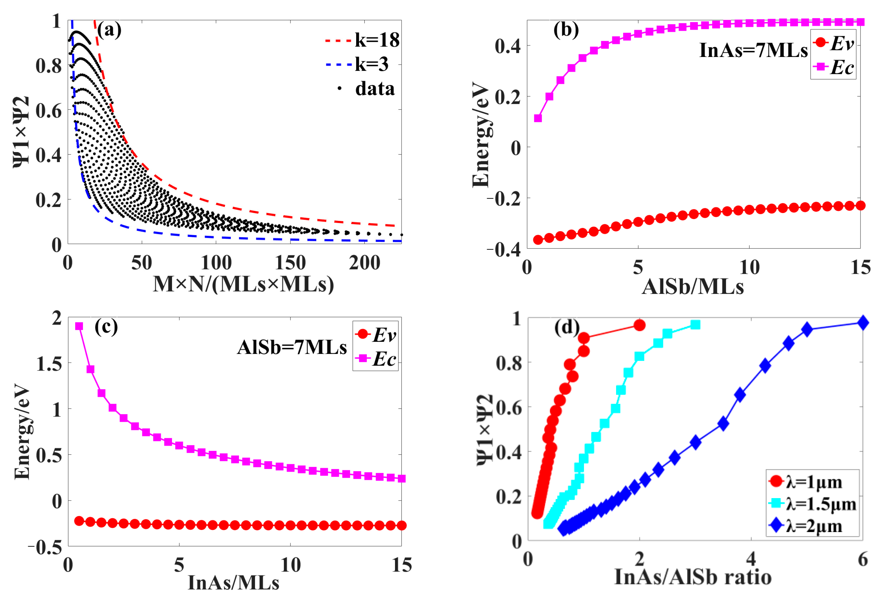
3.1. InAs/AlSb Superlattice

The WFO and absorption wavelengths of (M, N)-monolayer (ML) InAs/AlSb superlattices are calculated according to the above theoretical model. The relationship between the size of WFO and the superlattice layer thickness M × N is shown in Figure 1a. Among them, the WFO is proportional to k/(M × N), and the coefficient k is between 3 and 18. The simulation results are similar to those of InAs/GaSb superlattices. That is, when M × N is large enough, the intensity of the phototransition oscillator is proportional to 1/(M × N) [15]. Additionally, the electron-hole WFO of the superlattice is almost located at the interface. Furthermore, when the number of interfaces in the period is constant, the WFO would be larger with a smaller period thickness [23].
To study the relationship between the thickness of the InAs or AlSb layer and energy level. In the specific experiment, M and N increased sequentially from 0.5 MLs to 15 MLs, with each step of 0.5 ML (here, it is only necessary to ensure that 0.5 MLs is greater than the step value (0.01 nm) of the k·p algorithm). It can be seen from Figure 1b,c that the thickness of the InAs layer is unchanged. With the increase in AlSb, the conduction band gradually becomes stable after a rapid increase, and the valence band gradually becomes stable after a slow increase. On the other hand, the thickness of the AlSb layer is constant. With the increase in InAs, the conduction band decreases rapidly and then gradually becomes stable, and the valence band basically becomes stable. Therefore, the electron energy level affects and dominates the absorption wavelength. When the thickness of the InAs or AlSb layer changes, the electron energy level will change greatly, and the hole energy level shift will not exceed 0.1 eV [24].
Further, we also study the variation trend of the InAs/AlSb superlattice WFO under different layer thickness ratios of InAs/AlSb. These 1 μm and 1.5 μm are used as traditional low-loss windows for optical fiber communication. In addition, with the recent advance of detection and ranging systems in highly populated urban areas, eye safety has become a growing concern. The 2 µm window is ideal for LIDAR systems as it is considered eye-safe and effective in long-range detection [25]. For λ = 1 μm, λ = 1.5 μm, and λ = 2 μm, Figure 1d shows the WFO at different absorption wavelengths. The figure shows that the WFO increases with the increase in M/N. In order to achieve longer wavelength detection, the establishment of equivalent WFO requires a larger M/N value. Therefore, the absorption coefficient is enhanced by increasing the thickness of InAs and decreasing the thickness of AlSb. Moreover, the absorption wavelength of InAs/AlSb superlattices remains basically unchanged.
Both InAs or AlSb materials and GaSb substrates are stressed, so it is necessary to introduce an interfacial layer to balance the stress of the superlattice. The limitation of shutter control accuracy for molecular beam epitaxy needs to be considered. The WFO and absorption wavelength of InAs/AlSb superlattices in 7/2 MLs, 5/5 MLs, and 2/7 MLs are discussed in this paper. The above three examples are set as models A, B, and C, respectively. The WFO sizes were 0.81, 0.43, and 0.37, and the absorption wavelengths were 1.89 μm, 1.45 μm, and 0.99 μm, respectively.
InSb is usually introduced to regulate the tensile strain of the superlattice, and AlAs is usually introduced to regulate the compressive strain of the superlattice. In order to understand the influence of two interface layers’ thickness and position on the superlattice’s WFO and absorption wavelength. The following are specific simulations for three scenarios, including one or two interface layers of InSb (Section 3.2.1 and Section 3.2.2), one or two interface layers of AlAs (Section 3.3.1 and Section 3.3.2), and simultaneously introducing InSb and AlAs interface layers to adjust the stress balance.

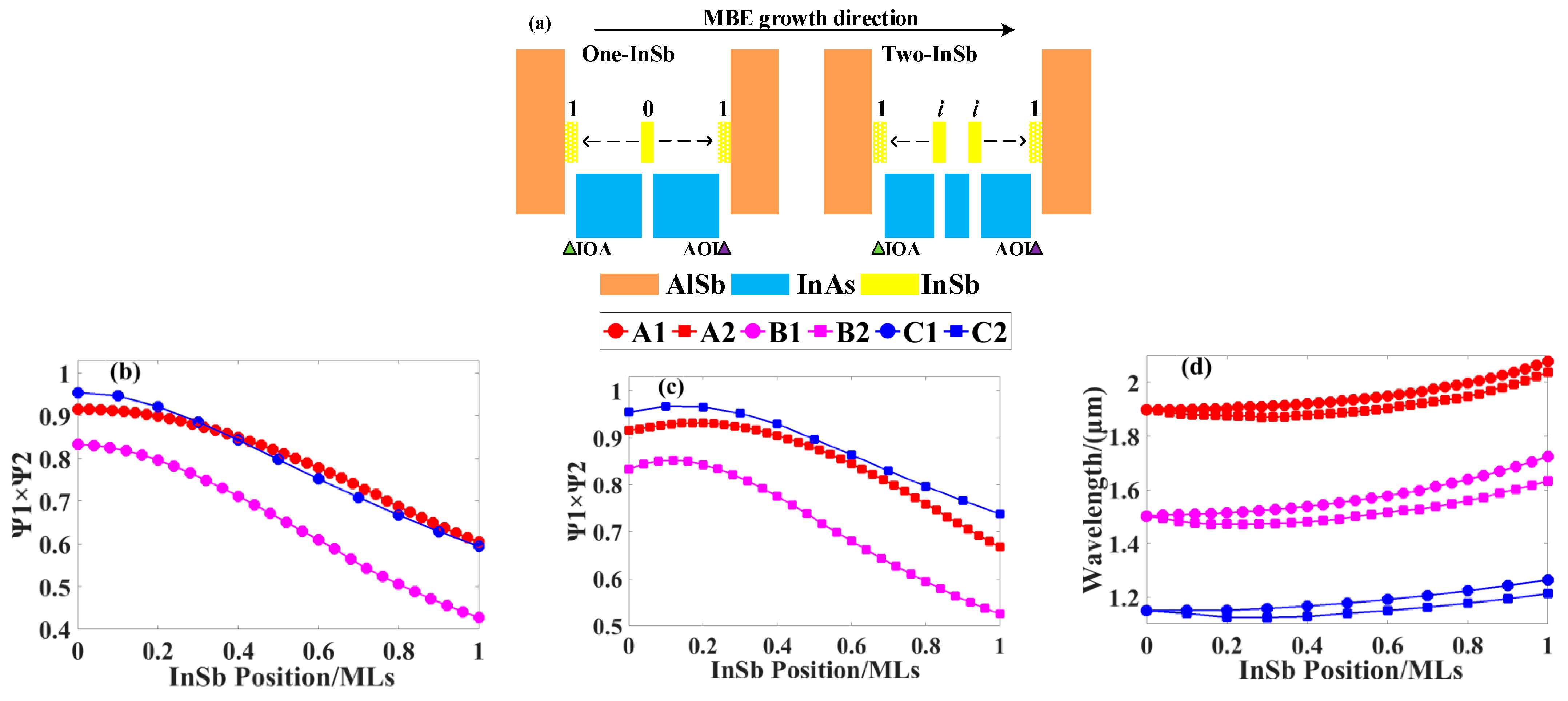
3.2. The Relationship between InSb Interface Layer and WFO

3.2.1. One Interface Layer of InSb

InSb is usually introduced to balance the stress between the InAs/AlSb superlattice and the substrate material with its larger lattice constant, and it shares group III elements In with InAs. Therefore, it is necessary to study the relationship between InSb material and the superlattice WFO, including the layer thickness of InSb and its position within the superlattice. We were considering inserting an InSb interface. The InAs-on-AlSb (IOA) interface should be set as the starting point, then steps along the epitaxial growth direction at intervals of 0.1 MLs of InAs can be taken. It ends at the AlSb-on-InAs (AOI) interface. Figure 2a shows on the left that the InSb is set to state 0 when it is in the middle of the InAs, and the InSb is set to state 1 when it is in the AOI (or IOA) interface. On this basis, the InSb thickness was increased from 0.1 MLs to 3 MLs at 0.1 MLs intervals. Table 2 summarizes the conditions of the three models for achieving maximum WFO. In addition, the simulation results also show that the WFO size is constant when the InSb interface layers have an equal distance to the middle of the InAs material.
The InSb insertion layer thicknesses of models A, B, and C were set at 0.6 MLs, 1.1 MLs, and 1.7 MLs, respectively. We studied the relationship between the location of InSb and WFO. Figure 2b shows the relationship between the position of InSb and WFO. The meaning of the horizontal coordinate is as follows: half of the InAs layer thickness is set as the unit length, the middle position is the state 0, and the AOI or IOA interface is the state 1. Models A1, B1, and C1 were introduced with an InSb interface. When the position of InSb moves towards the AOI (or IOA) interface, the electron-hole WFO tends to decrease. Specifically, the InAs within the InAs/AlSb superlattice form electron wells. Therefore, a small hole potential well is formed after the InSb interface is introduced, which makes the superlattice structure have an extra electron hole WFO. At the AOI or IOA interface of the InAs/AlSb superlattice, electrons and holes are tightly arranged alternately, but the electron-hole WFO is weakest at the 0 state, and the number of electrons in the InAs layer is greater than the number of holes. In order to maximize WFO, a certain InSb interface layer can be inserted at the 0 state to increase the probability of hole occupation.

3.2.2. Two Interface Layers of InSb

We have investigated the relationship between the introduction of two InSb interfaces in the InAs layer and the superlattice WFO. Model A takes the 0 state as the initial point and then inserts 0.3 MLs of InSb along the IOA interface and AOI interface directions, respectively. Figure 2a shows on the right the insertion examples of two InSb interface layers. The InSb of 0.55 MLs and 0.85 MLs were inserted into models B and C according to the simulation mode of model A, respectively. The relationship between the position of InSb and WFO is shown in Figure 3c, and here, the horizontal coordinate has the same meaning as (b). Models A2, B2, and C2 were introduced with two InSb interfaces. In Figure 3c, models A, B, and C have a WFO maximum between states 0 and 1 (positions i are 0.17, 0.12, and 0.1, respectively). We suspected that the optimal insertion position may be related to the layer thickness of InAs or InSb. Two InSb layers are more advantageous than one InSb layer because a small hole potential well is added so that the electron-hole WFO can be further enhanced. The WFO simulation results show that without considering strain balance conditions, the WFO of models A, B, and C can be increased from 0.81, 0.43, and 0.37 to 0.93, 0.85, and 0.97 after inserting two InSb layers.
Considering the introduction of interface layers, the structure of the superlattice has changed. Therefore, it is necessary to study the relationship between the InSb interface layer and the absorption wavelength. Figure 2d shows the wavelength drifts of models A, B, and C while being inserted into one or two InSb interfaces. The horizontal coordinate is the same as (b). The simulation results show that the wavelength shift of the superlattice is related to the position of InSb interfaces at a fixed InSb layer thickness. When one or two InSb layers are introduced into the superlattice, the shift range of the absorption wavelength is about ±0.3 μm. In addition, the wavelength change of InSb near state 0 is smaller than that of state 1. Therefore, the InSb at state 0 enhances the electron-hole WFO, and the absorption wavelength does not change significantly. In other words, the introduction of the InSb interface layer hardly affects the absorption wavelength of the superlattice and increases the WFO.

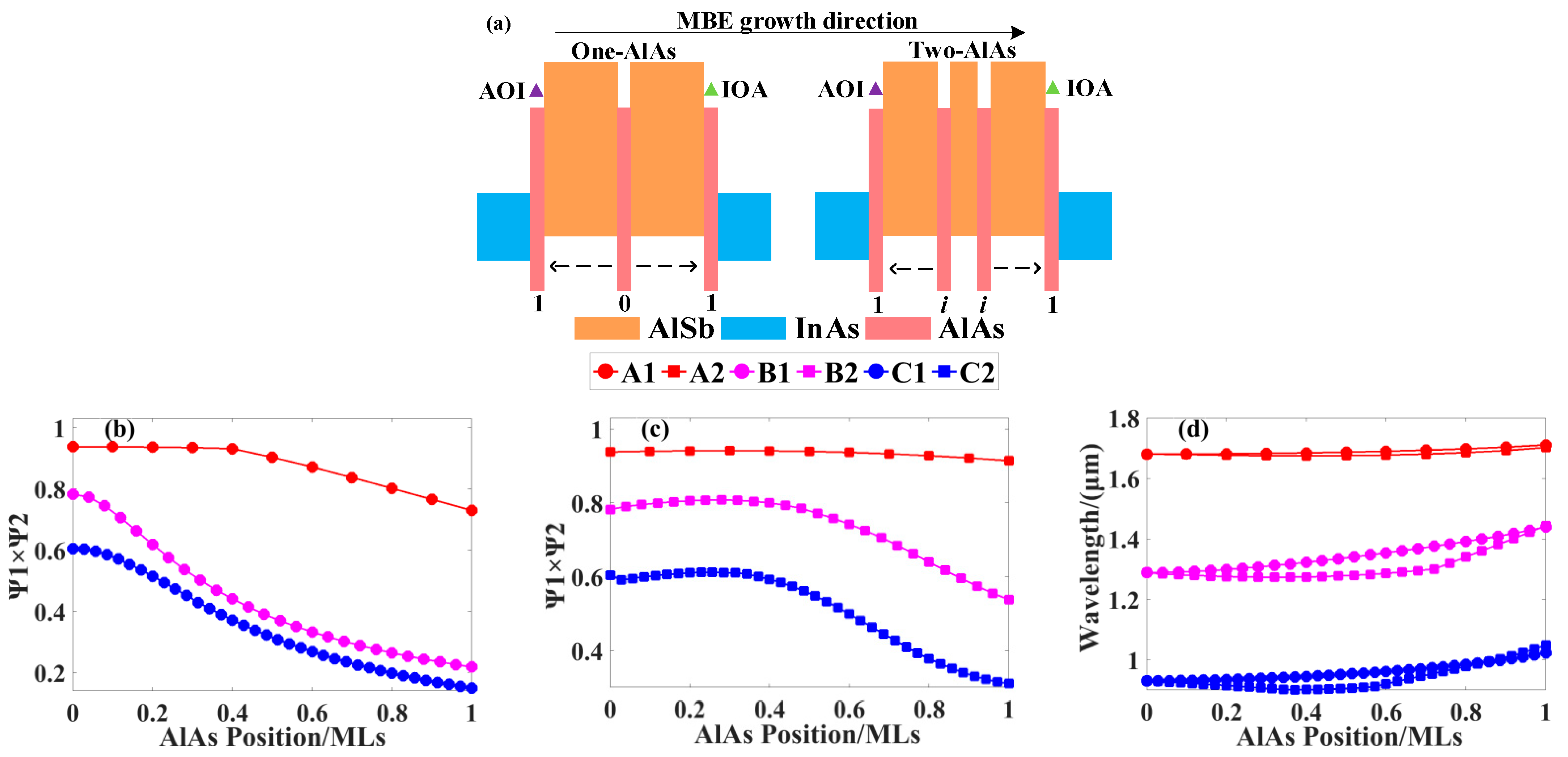
3.3. The Relationship between AlAs Interface Layer and WFO

3.3.1. One Interface Layer of AlAs

AlAs is usually introduced to balance the stress between the InAs/AlSb superlattice and the substrate material with its smaller lattice constant and share group III elements Al with AlSb. Similarly, the relationship between the superlattice’s WFO and AlAs material (the layer thickness of AlAs and its position within the superlattice) is analyzed. The specific simulation process is similar to InSb in Section 3.2.1. Table 3 shows that models A, B, and C can obtain a larger WFO after introducing a certain AlAs thickness at state 0. Then, by fixing the AlAs layer thickness, as shown on the left side of Figure 3a, one AlAs interface within the AlSb layer is inserted.
Figure 3b shows the relationship between the positions of AlAs and WFO. The meaning of the horizontal coordinate is as follows: half of the AlSb layer thickness is set as the unit length, the middle position is the state 0, and the AOI or IOA interface is the state 1. It is shown in Figure 3b that the electron-hole WFO tends to decrease as AlAs moves towards the AOI (or IOA) interface when the AlSb is within the InAs/AlSb superlattice form hole well. Therefore, a small electron potential well is formed after the InSb interface is introduced, which makes the superlattice structure have an extra electron-hole WFO. At the AOI or IOA interface of the InAs/AlSb superlattice, electrons and holes are tightly arranged alternately. However, the electron-hole WFO is weakest at the 0 state, and the holes in the AlSb layer are much larger than the electrons. In order to maximize WFO, a certain AlAs interface layer can be inserted in the 0 state to increase the probability of electron occupation.

3.3.2. Two Interface Layer of AlAs

Two AlAs interfaces are inserted into the AlSb layer for simulation analysis. The relationship between the position of AlAs and WFO is shown in Figure 3c, and here the horizontal coordinate has the same meaning as (b). In Figure 3c, the thicknesses of models A, B, and C inserted into AlAs are 0.5 MLs, 1.3 MLs, and 1.25 MLs, respectively. The simulation result is similar to the case when the InSb interface (in Section 3.2.2) is introduced; there is a WFO maximum value, but the specific position i is different, which is 0.3, 0.28, and 0.26, respectively. The WFO simulation results show that without considering strain balance conditions, the WFO of models A, B, and C can be increased from 0.81, 0.43, and 0.37 to 0.94, 0.81, and 0.61 after inserting two AlAs layers. Therefore, the electron-hole WFO is further enhanced.
Figure 3d shows the wavelength shifts of models A, B, and C while being inserted into one or two AlAs interfaces. The horizontal coordinate is the same as (b). The simulation results show that at a fixed AlAs layer thickness, the wavelength shift of the superlattice is related to the position of AlAs interfaces. When one or two AlAs interfaces are introduced into the superlattice, the absorption wavelength is blue-shifted by approximately 0.3 μm. In addition, the wavelength shift of the AlAs interface at state 0 is greater than that at state 1. This phenomenon of the AlAs interface is opposite to the simulation results of the InSb interface in Section 3.2.2. Although AlAs enhances the electron-hole WFO at state 0, the absorption wavelength is blue-shifted, which is still within the allowed range.

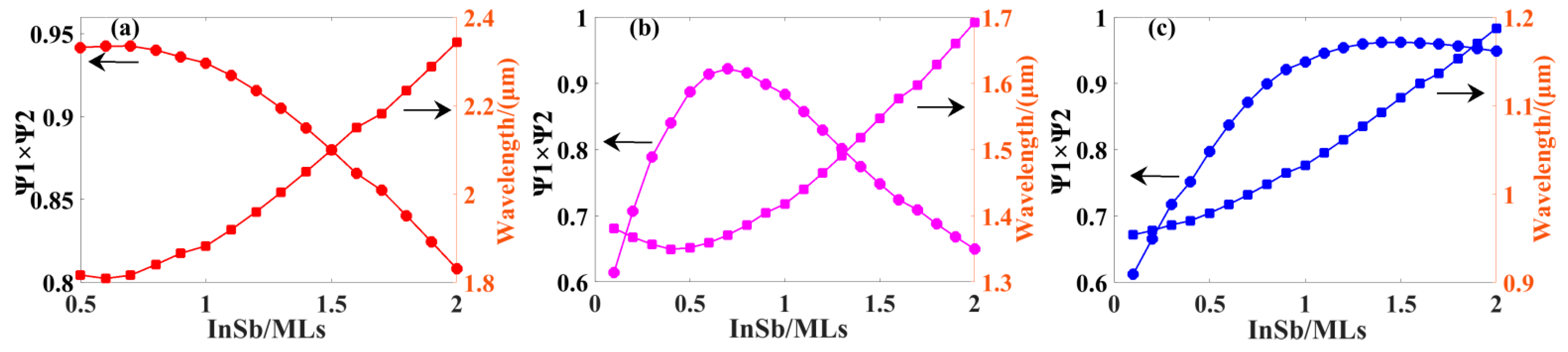
3.4. The Relationship between Stress-Balance-Based Interface Engineering and the Size of Electron-Hole WFO

Based on the above simulation results, it can be seen that introducing two interfaces with the same thickness can significantly enhance WFO. However, the defect can be easily generated, which may lead to low QE in superlattices with multiple interfaces realized with MBE. In addition, when an interface layer of certain thickness is introduced, WFO at state 0 enhances more significantly, yet WFO near state 1 is weakened. Therefore, at state 0, the relationship between the thickness of an interface layer and the size of WFO is considered. Figure 4a,b show the layer thickness variations of the InSb and AlAs interfaces, respectively. The results show that WFO enhances rapidly with the increase in AlAs thickness and then stabilizes. Furthermore, the WFO variation is not obvious when the AlAs interface is too thick, which means that an ultra-thick AlAs interface layer cannot effectively enhance absorption. Therefore, it is recorded in Table 3 of Section 3.3.1 that the required AlAs layer thicknesses of models A, B, and C are 1 MLs, 2.6 MLs and 2.5 MLs, respectively, and then the WFO of each model reaches the maximum value. However, when the thickness of the InSb interface layer continuously increases, the WFO will decrease after it increases to a certain extent. This phenomenon leads to lower tolerance during experimental demonstrations, and the WFO may be reduced. Therefore, in order to enhance electron-hole WFO in actual epitaxy, it is more suitable to introduce the AlAs layer than the InSb layer [19]. It is recorded in Table 2 of Section 3.2.1 that the required InSb layer thicknesses of models A, B, and C are 0.6 MLs, 1.1 MLs, and 1.7 MLs, respectively, and then the WFO of each model reaches the maximum value.
Based on the actual epitaxy, there are lattice mismatches among InAs, AlSb, and GaSb substrates. Although the interface layer enhances the electron-hole WFO of the InAs/AlSb superlattice, there is a sharp increase in the stress of the InAs/AlSb superlattice with the increase in interface layer thickness. Therefore, it is necessary to introduce the InSb and AlAs interface layers to balance the stress. According to the lattice constants of binary compounds, the matching conditions of models A, B, and C and the GaSb lattice are analyzed, respectively. Here, each model introduces x InSb and y AlAs, where the coefficients x and y need to meet the following conditions:
y = 0.8967 x 0.0771 m + 0.1028 n
where m and n are the atomic layer thicknesses of InAs and AlSb, respectively, in the model. Therefore, if the interfacial layer thickness x of InSb is fixed, the unique corresponding AlAs interfacial layer thickness y( y = K x + b ) can be calculated. The relationship of coefficients K and b between x and y in models A, B, and C is shown in Table 4.
The variation of WFO size is studied by increasing InSb layer thickness under stress balance conditions. Figure 5a–c shows the WFO maxima of models A, B, and C, respectively. With the increase in the InSb interface, WFO shows a trend of first increasing and then decreasing. For these three models, WFO enhances them overall. Model A introduces 0.7 ML of InSb and 0.3 ML of AlAs, respectively, and the WFO size increases from 0.81 to 0.94, with a wavelength blue-shift of 0.07 μm. Similarly, the thickness of the InSb and AlAs layers is introduced according to Table 3. The WFO of model B is enhanced from 0.43 to 0.92, and the wavelength red-shift is 0.12 μm. The WFO of model C is enhanced from 0.37 to 0.96, and the wavelength red-shift is 0.12 μm. According to the simulation results, the WFO of each model can reach more than 0.9, and the wavelength shift is about 0.1 μm. Therefore, InSb and AlAs are chosen for the interface engineering, which can significantly enhance the WFO without affecting the absorption wavelength.
Table 5 shows that WFO is enhanced to different degrees after superlattice materials are inserted into the interface layer, which is finally reflected in the enhancement of photoluminescence (PL), absorption coefficient, QE, and other optical properties. Similarly, there may be predictable optical property (QE) enhancement after the insertion of InSb or AlAs into the InAs/AlSb superlattice materials.

4. Conclusions

In summary, this article discusses the effects of InSb and AlAs interface layers on different InAs/AlSb superlattice models, including parameters with WFO and absorption wavelength. When two InSb interfaces are introduced, the WFO size of models A, B, and C is increased by 14.8%, 97.7%, and 162.2%, and the wavelength red-shift is 0.19 μm, 0.27 μm, and 0.28 μm, respectively. When two AlAs interfaces are introduced, the WFO size of models A, B, and C is increased by 16.2%, 87.8%, and 65.4%, respectively. The absorption wavelength has a blue-shift of about 0.3 μm. Considering the actual epitaxy difficulty of multiple interfaces, we designed interface engineering by introducing InSb and AlAs interface layers within the InAs/AlSb superlattice. By adjusting the thickness of the InSb and AlAs interfaces, the maximum WFO of models A, B, and C can be increased by 16%, 114%, and 159.5%. There is a maximum value of WFO in the simulation based on interface engineering, and the size of WFO meets the trend of first increasing and then decreasing. This phenomenon is related to the introduction of InSb interface layers, so the WFO size of the InAs/AlSb superlattice depends on the thickness of the InSb interface layer. In addition, the absorption wavelength fluctuates around 0.1 μm, and the introduction of interface engineering hardly affects the detection wavelength of the detector. In the next step, we will grow InAs/AlSb superlattices with high absorption coefficients through molecular beam epitaxy devices and then make avalanche photodetectors to verify optical and electrical properties.

Author Contributions

Conceptualization, L.Z., L.L., Y.F. and J.O.; methodology, J.Y.; software, W.C., X.Z. and D.Z.; validation, J.Y., L.L. and W.C.; formal analysis, L.Z., Y.F. and J.O.; investigation, L.L., X.Z. and D.Z.; resources, L.Z., Y.F. and J.O.; data curation, J.Y.; writing—original draft preparation, J.Y.; writing—review and editing, J.Y., L.L. and W.C. All authors have read and agreed to the published version of the manuscript.

Funding

This research was funded by The Research Project of Beijing Municipal Natural Science Foundation (No.BJXZ2021-012-00046) and the National Natural Science Foundation of China (62205029) (2022YFF0705800).

Data Availability Statement

The data supporting this study’s findings are available within the article.

Conflicts of Interest

The authors declare no conflict of interest.

References

  1. John, E.B.; Anand, R.; Dai, D.X.; Wissem, S.Z.; Yimin, K.; Tao, Y.; Mike, M. Recent advances in Ge/Si PIN and APD photodetectors. Phys. Status Solidi C 2010, 7, 2526–2531. [Google Scholar] [CrossRef]
  2. Sieck, A.; Benecke, M.; Eich, D.; Oelmaier, R.; Wendler, J.; Figuregemeier, H. Short-Wave Infrared HgCdTe Electron Avalanche Photodiodes for Gated Viewing. J. Electron. Mater. 2018, 47, 5705–5714. [Google Scholar] [CrossRef]
  3. MohammadNejad, S.; Aghaei, F. Noise characteristics improvement of submicron InP/InGaAs avalanche photodiode for laser detection system. Opt. Commun. 2020, 455, 124561. [Google Scholar] [CrossRef]
  4. Ronningen, T.J.; Kodati, S.H.; Jin, X.; Lee, S.; Jung, H.; Tao, X.; Lewis, H.I.J.; Schwartz, M.; Gajowski, N.; Martyniuk, P.; et al. Ionization coefficients and excess noise characteristics of AlInAsSb on an InP substrate. Appl. Phys. Lett. 2023, 123, 131110. [Google Scholar] [CrossRef]
  5. Zederbauer, T.; Andrews, A.M.; MacFarland, D.; Detz, H.; Schrenk, W.; Strasser, G. Enhanced Crystal Quality of AlxIn1−xAsySb1−y for Terahertz Quantum Cascade Lasers. Photonics 2016, 3, 20. [Google Scholar] [CrossRef]
  6. Campbell, J.C.; David, J.P.R.; Bank, S.R. Sb-Based Low-Noise Avalanche Photodiodes. Photonics 2023, 10, 715. [Google Scholar] [CrossRef]
  7. Kodati, S.H.; Lee, S.; Guo, B.; Jones, A.H.; Schwartz, M.; Winslow, M.; Pfiester, N.A.; Grein, C.H.; Ronningen, T.J.; Campbell, J.C.; et al. AlInAsSb avalanche photodiodes on InP substrates. Appl. Phys. Lett. 2021, 118, 091101. [Google Scholar] [CrossRef]
  8. Jones, A.H.; March, S.D.; Bank, S.R.; Campbell, J.C. Low-noise high-temperature AlInAsSb/GaSb avalanche photodiodes for 2-μm applications. Nat. Photonics 2020, 14, 559–563. [Google Scholar] [CrossRef]
  9. Jones, A.H.; March, S.D.; Dadey, A.A.; Muhowski, A.J.; Bank, S.R.; Campbell, J.C. AlInAsSb Separate Absorption, Charge, and Multiplication Avalanche Photodiodes for Mid-Infrared Detection. IEEE J. Quantum Electron. 2022, 58, 1–6. [Google Scholar] [CrossRef]
  10. Adam, A.; Dadey, J.; Andrew, M.A.; Abhilasha, K.; Seth, R.; Bank, D.W.; Joe, C.C. High-gain low-excess-noise MWIR detection with a 3.5-µm cutoff AlInAsSb-based separate absorption, charge, and multiplication avalanche photodiode. APL Photonics 2023, 8, 036101. [Google Scholar] [CrossRef]
  11. Maddox, S.J.; March, S.D.; Bank, S.R. Broadly Tunable AlInAsSb Digital Alloys Grown on GaSb. Cryst. Growth Des. 2016, 16, 3582–3586. [Google Scholar] [CrossRef]
  12. Chang, F.R.; Hao, R.T.; Qi, T.T.; Zhao, Q.C.; Liu, X.X.; Li, Y.; Gu, K.; Guo, J.; Wang, G.W.; Xu, Y.Q. High material quality growth of AlInAsSb thin films on GaSb substrate by molecular beam epitaxy. Chin. Phys. B 2019, 28, 445–449. [Google Scholar] [CrossRef]
  13. Ren, M.; Maddox, S.J.; Woodson, M.E.; Chen, Y.J.; Bank, S.R.; Campbell, J.C. Characteristics of AlxIn1−xAsySb1−y (x: 0.3–0.7) Avalanche Photodiodes. J. Light. Technol. 2017, 35, 2380–2384. [Google Scholar] [CrossRef]
  14. Min, R.; Scott, J.M.; Madison, E.W.; Chen, Y.j.; Seth, R.B.; Campbell, J.C. AlInAsSb separate absorption, charge, and multiplication avalanche photodiodes. Appl. Phys. Lett. 2016, 108, 191108. [Google Scholar] [CrossRef]
  15. Chang, Y.C.; Schulman, J.N. Interband optical transitions in GaAs-Ga1−xAlxAs and InAs-GaSb superlattices. Phys. Rev. B 1985, 31, 2069. [Google Scholar] [CrossRef]
  16. Nguyen, B.M.; Hoffman, D.; Delaunay, P.Y.; Razeghi, M. Dark current suppression in type II InAs/GaSb superlattice long wavelength infrared photodiodes with M-structure barrier. Appl. Phys. Lett. 2007, 91, 163511. [Google Scholar] [CrossRef]
  17. Wu, Y.Y.; Zhang, Y.H.; Zhang, Y.; Zhao, Y.H.; Zhang, Y.; Xu, Y.Q.; Liang, C.Y.; Niu, Z.C.; Shi, Y.; Che, R.C. Dual strategy of modulating growth temperature and inserting ultrathin barrier to enhance the wave function overlap in type-II superlattices. Nano Res. 2022, 15, 5626–5632. [Google Scholar] [CrossRef]
  18. Zhao, Y.H.; Liu, L.; Bi, H.; Han, X.; Zhao, X.B.; Ni, H.Q.; Xu, Y.Q.; Niu, Z.C.; Che, R.C. Quantum efficiency optimization by maximizing wave function overlap in type-II superlattice photodetectors. Nanoscale 2017, 9, 11833–11840. [Google Scholar] [CrossRef]
  19. Cai, C.Y.; Zhao, Y.H.; Chang, Y.R.; Zhao, X.B.; Yang, L.B.; Liang, C.Y.; Wang, G.W.; Niu, Z.C.; Shi, Y.; Liu, X.H.; et al. Understanding the role of interface in advanced semiconductor nanostructure and its interplay with wave function overlap. Nano Res. 2020, 13, 1536–1543. [Google Scholar] [CrossRef]
  20. Vurgaftman, I.; Meyer, J.R.; Ram-Mohan, L.R. Band parameters for IIIV compound semiconductors and their alloys. J. Appl. Phys. 2001, 89, 5815–5875. [Google Scholar] [CrossRef]
  21. Qiao, P.F.; Shin, M.; Shun, L.C. Electronic band structures and optical properties of type-II superlattice photodetectors with interfacial effect. Opt. Express 2012, 20, 2319–2334. [Google Scholar] [CrossRef]
  22. Xia, J.B.; Zhu, B.F. Semiconductor Superlattice Physics; Science and Technology Press: Shanghai, China, 1995; p. 388. [Google Scholar]
  23. Kroemer, H. The 6.1Å family (InAs, GaSb, AlSb) and its heterostructures: A selective review. Physica E 2004, 20, 196–203. [Google Scholar] [CrossRef]
  24. Zheng, J.; Andrew, H.J.; Tan, Y.H.; Rockwell, A.K.; Stephen, M.; Sheikh, Z.A.; Catherine, A.D.; Avik, W.G.; Seth, R.B.; Campbell, J.C. Characterization of band offsets in AlxIn1−xAsySb1−y alloys with varying Al composition. Appl. Phys. Lett. 2019, 115, 122105. [Google Scholar] [CrossRef]
  25. Scholle, K.; Lamrini, S.; Koopmann, P.; Peter, F. 2 µm laser sources and their possible applications. In Frontiers in Guided Wave Optics and Optoelectronics; IntechOpen: London, UK, 2010. [Google Scholar] [CrossRef]
  26. Webster, P.T.; Riordan, N.A.; Liu, S.; Steenbergen, E.H.; Synowicki, R.A.; Zhang, Y.H.; Johnson, S.R. Absorption properties of type-II InAs/InAsSb superlattices measured by spectroscopic ellipsometry. Appl. Phys. Lett. 2015, 106, 061907. [Google Scholar] [CrossRef]
  27. Bi, H.; Han, X.; Liu, L.; Zhao, Y.; Zhao, X.; Wang, G.; Xu, Y.; Niu, Z.; Shi, Y.; Che, R. Atomic Mechanism of Interfacial-Controlled Quantum Efficiency and Charge Migration in InAs/GaSb Superlattice. ACS Appl. Mater. Interfaces 2017, 9, 26642–26647. [Google Scholar] [CrossRef]
Figure 1. (a) InAs and AlSb were linearly combined at intervals of 0.5 MLs for thicknesses ranging from 0.5 MLs to 15 MLs. The ordinate is expressed as the relationship between the size of the WFO and the inverse proportional coefficient k. The abscissa is the product of InAs and AlSb thickness. (b) When the thickness of InAs is 7 MLs, the relationship between the energy level of the superlattice and the thickness of the AlSb layer. (c) When the thickness of AlSb is 7 MLs, the relationship between the energy level of the superlattice and the thickness of the InAs layer. (d) When the absorption wavelength is 1 μm, 1.5 μm, and 2 μm, the ratio of InAs and AlSb layer thickness is related to the WFO.
Photonics 10 01268 g001
Figure 2. (a) The position of the InSb interface layer in the InAs layer. (b) Models A1, B1, and C1 introduce an InSb interface. (c) Models A2, B2, and C2 introduce two InSb interfaces. (d) The wavelength shift of the superlattice after inserting one or two InSb interfaces into the InAs layer.
Photonics 10 01268 g002
Figure 3. (a) The position of the AlAs interface layer in the AlSb layer. (b) Models A1, B1, and C1 introduce an AlAs interface. (c) Models A2, B2, and C2 introduce two AlAs interfaces. (d) The wavelength shift of the superlattice after inserting one or two InSb interfaces into the InAs layer.
Photonics 10 01268 g003
Figure 4. (a) The relationship between the WFO size of models A, B, and C and the InSb layer thickness at state 0. (b) The relationship between the WFO size of models A, B, and C and the AlAs layer thickness at state 0.
Photonics 10 01268 g004
Figure 5. In models A, B, and C, AlAs follows the InSb interface, which ensures stress balance. (a) The relationship between the thickness of the InSb layer and the WFO, as well as the absorption wavelength of Model A. (b) The relationship between the thickness of the InSb layer and the WFO, as well as the absorption wavelength of Model B. (c) The relationship between the thickness of the InSb layer and the WFO, as well as the absorption wavelength of Model C.
Photonics 10 01268 g005
Table 1. Some material parameters for the 8-band k·p method.
ParameterSymbolInAsAlSbInSbAlAs
Luttinger parameters γ 1 L 19.44.1532.43.76
γ 2 L 8.5451.2813.31.23
γ 3 L 9.171.7515.151.42
Corrected Luttinger parameters γ 1 6.31.7616.780.737
γ 2 1.990.0855.610.125
γ 3 2.620.557.460.315
Table 2. The insertion position and layer thickness parameters of InSb when maximizing the WFO of models A, B, and C.
ModelPositionInSb ThickPosition-iInSb Thick
A00.6 MLs0.170.3 MLs
B01.1 MLs0.120.55 MLs
C01.7 MLs0.100.85 MLs
Table 3. The insertion position and layer thickness of AlAs when maximizing the WFO of models A, B, and C.
ModelPositionAlAs ThickPosition-iAlAs Thick
A01 MLs0.30.5 MLs
B02.6 MLs0.281.3 MLs
C02.5 MLs0.261.25 MLs
Table 4. Stress balance parameters and interface atomic layer thickness of optimal WFO under different models.
ModelKbInSb/MLsAlAs/MLs
A0.8967−0.33410.70.3
B0.12850.70.8
C0.56541.51.9
Table 5. Relationship between interface layer and optical performance.
Materials/MLsDataInterface LayerThick/ÅWFOQEImprove
8InAs/7.5AlSb [17]ExperimentAlAs3.44Enhance-PL improved 50%
35InAs/10AlSb [19]ExperimentInAsSb1.51Enhance-Optical performance
17InAs/15InAsSb [26]SimulationInAsSb6.03Enhance 652%-absorption coefficient improved 683%
InAs/GaSb [27]ExperimentInSb~3Enhance23% to 50%QE improved 117%
This paper 5InAs/5AlSbSimulationAlAs, InSb2.26, 2.27 Enhance 114%-Optical performance
Disclaimer/Publisher’s Note: The statements, opinions and data contained in all publications are solely those of the individual author(s) and contributor(s) and not of MDPI and/or the editor(s). MDPI and/or the editor(s) disclaim responsibility for any injury to people or property resulting from any ideas, methods, instructions or products referred to in the content.

