1. Introduction
Wideband electromagnetic absorbing materials play an important role in electromagnetic shielding and radar stealth. Metamaterials, as a kind of artificial medium capable of controlling electromagnetic waves [
1,
2], offer a novel approach for constructing absorbing materials. Compared with traditional absorbing materials, metamaterial absorbers possess distinct advantages, including low profile, lightweight, and high absorptivity [
3]. The exploration of metamaterial absorbers has evolved from the microwave domain to encompass the THz and optical spectra. Significant progress has been made in achieving metamaterial absorbers with wideband absorption, polarization insensitivity, and wide incident angle [
4,
5,
6,
7,
8,
9,
10].
In recent years, multi-functional metamaterial absorbers, such as high Q-factor perfect absorbers, full-stokes polarization perfect absorption metasurfaces, and so on [
11,
12], have received widespread attention from the scientific and engineering communities [
13,
14,
15,
16,
17,
18]. The endeavor to improve communication security and reduce radar cross-section has underscored the practical significance of devising metamaterial absorbers incorporating transmission windows. The typical structure of such metamaterial absorbers with a transmission window includes a lossy structural layer on the top and a lossless frequency-selective surface on the bottom. The absorption property is achieved through the plane metal structure loaded with lossy electronic components in the lossy structural layer, while the transmission window is realized using the lossless frequency-selective surface. Frequency-selective surfaces have the property of frequency-selective characteristics. When bandpass frequency-selective surfaces are applied to electromagnetic target stealth design, it can initiate the incident wave transmission at the predesigned frequency band. However, out-of-band signals are usually blocked and reflected in other directions, which will increase the chances of being detected. If we combine the metamaterial absorbers with the frequency-selective surface, it will be able to transmit waves at the predesigned frequency band, while absorbing waves at the other frequency band, which will undoubtedly greatly reduce the chances of being detected of the electromagnetic targets. With the fast development of tunable metamaterial absorbers, the metamaterial absorbers with switchable transmission windows have obtained considerable attention. Numerous kinds of metamaterial absorbers with switchable wave transmission windows have been proposed over the last several years [
19,
20,
21,
22]. For instance, Han et al. designed a metamaterial absorber with a transmission window based on a slot array and a PIN diode [
19], showing absorption exceeding 90% from 1.79 to 5.25 GHz, with an insertion loss of −1.28 dB at 3.68 GHz. Similarly, Ghosh et al. devised a metamaterial absorber endowed with a switchable transmission window, leveraging a PIN diode [
20]. When the diodes were forward-biased, the absorption exceeded 90% within the range of 3 to 7.82 GHz, while the transmission window manifested at 9.28 GHz during reverse-biased operation of the PIN diodes. Additionally, in 2020, Qu et al. proposed a bipolar fossil graphene-based multifunctional metamaterial absorber [
21]. By tuning the Fermi levels of the two graphene layers to 1 eV and 0 eV, the absorber exhibited a wave transmission window at 0.63 THz. On the other hand, adjusting the Fermi levels to 0 eV and 1 eV resulted in absorption levels exceeding 90% from 0.29 to 0.91 THz. On the basis of predecessors, in 2021, S C. Bakshi et al. conceived a metamaterial absorber embedding a transmission window by employing diodes in two layers [
22]. In the reverse-biased condition, the absorber achieved absorption levels exceeding 90% within the frequency ranges of 2.9 to 5.4 GHz and 6.3 to 8.2 GHz, with a transmission window appearing at 5.8 GHz. Furthermore, operating the diodes in the forward-biased condition led to absorption levels exceeding 90% over the frequency band of 2.85 to 8.11 GHz.
The previously discussed metamaterial absorbers featuring switchable transmission windows predominantly rely on the utilization of PIN diodes or graphene. Due to the high insertion loss of PIN diodes at the THz band, it cannot be used to realize metamaterial absorbers featuring a switchable function at the THz band. Although graphene can be used to achieve reconfigurable THz metamaterial, the circuit which is used to apply voltage on graphene is very complex. In this paper, we demonstrate an optically reconfigurable metamaterial with switchable wideband absorption and transmission based on the optically controlled conductivity of silicon in the THz frequency band. This design exhibits promising application potential in fields such as stealth communication equipment and radar operating in the THz frequency band.
2. Design Principle
When we use FR-4 dielectric-copper-clad plate to realize metamaterial absorbers, the equivalent resistance of the metal and loss dielectric layer is not significant, and the relative bandwidth which is achievable by a single resonant structure is only about 5%. The parameter changes of the resonant metal structure are mainly for adjusting resonant frequency; complex resonant metal structure can only achieve a combination of resonant frequency between a limited number of structures, making it difficult to achieve tens of fold changes. The change in dielectric material loss involves material science, and it is difficult to make significant breakthroughs. Therefore, the way to expand bandwidth in terms of magnitude is to introduce patch resistors or resistive film. By loading the chip resistor or resistive film, it can increase the equivalent resistance R and reduce the quality factor Q of metamaterial absorbers by ten thousand times, and then reduce the sensitivity of circuit resonance to frequency; as a result, it can achieve wideband metamaterial absorbers.
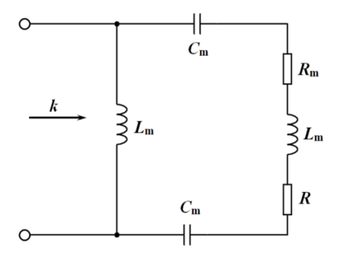
The equivalent circuit model of the wideband metamaterial absorbers loaded with resistive film is shown in
Figure 1, where
Rm is the loss resistance of the top resonant unit,
R is the resistance of lumped resistor, and
Lm and
Cm, respectively, represent the mutual inductance and capacitance between the top resonant unit and the bottom metal ground plate. The input impedance of this circuit can be expressed as follows:
Its resonant frequency
ω0, quality factor
Q, and passband
BW can, respectively, be expressed by the following:
It can be seen from Formula (4) that the absorption band of metamaterial absorbers can be widened when the resistance film is loaded.
The purpose of the bottom metal ground plate at the metamaterial absorbers is to prevent the incident wave transmission. The frequency-selective surface has the property of frequency filtering characteristics. It can transmit the incident wave at the predetermined frequency band [
10]. If, instead, we use the bottom metal ground plate with the frequency-selective surface at the resistive-film metamaterial absorbers, it can realize the transmission of the incident wave at the predetermined frequency band and wideband absorption at the other frequency band. On this basis, if we fill the open slots at the frequency-selective surface with silicon, which has the property of the pump-power-dependent conductivity at the THz band, it can realize the reconfigurable THz metamaterial, transmitting the incident wave at the predetermined frequency band when the conductivity of silicon is very low, and wideband absorption at the other frequency band when the conductivity of silicon is very high.
3. Model Design
The unit cell of the proposed metamaterial with a switchable transmission window is schematically illustrated in
Figure 2. The metamaterial consists of three layers: a split gold ring loaded with resistive film (the conductivity
σ = 11 S/m) at the top, a polyimide substrate (permittivity
ε = 3.5 and loss tangent tanδ = 0.0027) in the middle, and a gold ground plane with square open slots filled with silicon (the permittivity
ε = 11.7, the pump-power-dependent conductivity
σsi) at the bottom [
23]. The thickness of both the top and bottom layer is set at 0.02 μm, while the middle layer has a thickness of 2 μm. The optimized structural parameters are as follows:
a =
b = 14 μm;
r = 5 μm;
c =
d = 1 μm;
e = 10 μm; and
f = 1 μm.
In terms of desirable properties at the THz band, gold has a certain degree of flexibility and is incorruptible, so it is the best metal material for achieving terahertz metamaterial absorbers. At practical applications, there are various curved surfaces, and the metamaterial absorbers are not only requires to absorb the incident wave at a wideband frequency; they are also required to be flexible. Traditional stealth coatings can be coated on curved surfaces by spraying, but the coatings are prone to detachment in harsh environments and have high maintenance costs. Additionally, stealth coatings have the drawbacks of large weight and narrow absorption bands. Although metamaterial absorbers made of FR-4 material can realize wideband absorption, such rigid structures have great difficulties in fitting curved surfaces. Therefore, it is necessary to design flexible metamaterial absorbers to meet the stealth requirements of curved surfaces. The current flexible metamaterial absorbers mainly rely on changing the material of the intermediate medium layer to achieve wideband absorption using rubber or similar materials. The overall thickness is often great, making them difficult to apply in equipment with limited volume. At the same time, in applications such as the wild, free space, and such, they are not suitable for carrying heavy objects, and thick and bulky metamaterial absorbers are even more difficult to use. To address the above issues, polyimide is one of the best selections with respect to thin-film insulation materials. Polyimide thin films have excellent bearing capacity with respect to high and low temperatures and electrical insulation and can be used for a long time over a wide temperature range, making them particularly suitable as substrates for flexible metamaterial absorbers.
When external pump power is applied and the conductivity of silicon reaches 50,000 S/m, the bottom gold plane with a silicon-filled open slot can be treated as a metal plane. In this state, incident waves are prevented from transmitting through the absorbers, and the front resonant layer absorbs the incident waves without reflection. On the other hand, when the applied external pump power is reduced to achieve a silicon conductivity of 150 S/m, the bottom gold plane with a silicon-filled open slot can be perceived as a frequency-selective surface, which can transmit incident waves at the working frequency. If the photoexcitation of metamaterial silicon regions is achieved using the near-infrared laser pulse with a center wavelength of 800 nm, then the fitted dependence of the silicon conductivities on the power of the pump beam can be expressed approximately as
according to the experimental result in ref. [
24], where
I (mW) is the power of pump optical beam [
24].
Figure 3 shows the experimental and fitted dependence of the silicon conductivity on pump power; it indicates that the fitted results are mostly same as the experimental results in ref. [
24]. This relationship is based solely on the silicon property; so, it is still valid for a different metamaterials structure. According to the above fitted formula, the pump beam power with the conductivity of silicon 50,000 S/m and 150 S/m are 500 mW and 0.9 mW, respectively.
The theoretical basis of the CST Microwave Studio is the FIT (finite integral technique), which is directly derived from Maxwell’s equations from a solution perspective. Therefore, CST Microwave Studio can calculate time-domain solutions and is very suitable for the simulation of passive devices. By utilizing the S parameters of each unit in the system, it can quickly analyze and reduce the memory required for the system. Moreover, CST Microwave Studio can basically cover the entire electromagnetic wave frequency band, covering both time-domain and frequency-domain solutions, and has multiple full-wave and high-frequency algorithms. Based on the above advantages, the electromagnetic performance of the proposed metamaterial was numerically investigated using the commercial software CST Microwave Studio. In the simulation, periodic boundary conditions were applied along the x and y directions, and an open boundary was set along the z direction. The All+Floquet modes are used to simulate the incident waves, and the frequency domain calculation method is used to calculate and analyze the electromagnetic characteristics of the metamaterial.
4. Results and Discussion
Figure 4a shows the S parameters and absorptivity of the metamaterial when the conductivity of silicon is 50,000 S/m. Under this condition, the transmission (
S21) is limited to a low level, while the absorptivity exceeds 90% from 3.1 to 10 THz, with a relative bandwidth over 105%.
Figure 4b depicts the S parameter of the metamaterial with the silicon conductivity of 150 S/m. One sees that a transmission peak obviously appears at 5.12 THz, with a transmission coefficient of 61%. The results indicate that the proposed metamaterial exhibits the multi-functionality of switchable wideband absorption and transmission. Notably, the transmission frequency lies within the absorption band, which holds significant implications for practical applications. The switchable wideband absorption and transmission can be attributed to the unique properties of silicon, which can be effectively considered as a metal when its conductivity reaches 50,000 S/m. Our designed model is a typical metamaterial, and the loaded resistive film can realize wideband absorption in this case. Conversely, under a silicon conductivity of 150 S/m, the bottom layer of the metamaterial functions as a frequency-selective surface, enabling narrowband transmission [
10].
Figure 5 shows the S parameters of the metamaterial without silicon. It indicates that the transmission of the metamaterial is basically same, with a silicon conductivity of 150 S/m.
The absorption mechanism of the metamaterial can be attributed to its impedance matching with free space.
Figure 6 shows the ratio of normalized input impedance of the metamaterial to that of free space when the conductivity of silicon is 50,000 S/m, which is calculated via the scattering parameter method [
25]. It is seen that the normalized input impedance of the metamaterial is basically equal to the equivalent impedance of free space from 3.1 to 10 THz. Consequently, the metamaterial absorber achieves a decent impedance match with free space, meeting the precondition of wideband absorption.
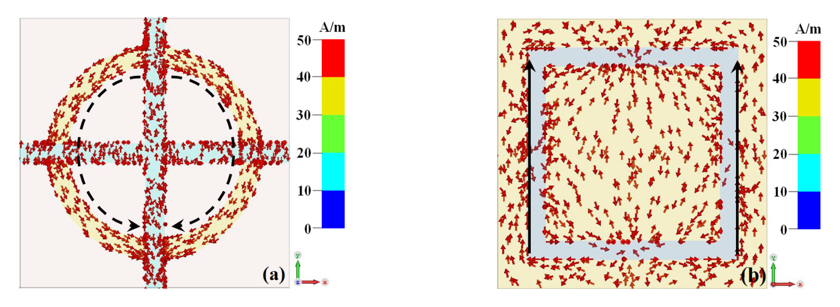
To deeply explore the mechanism of wideband absorption of the metamaterial with a silicon conductivity of 50,000 S/m, we monitor the surface current distributions at 8 THz, as shown in
Figure 7. The surface currents on the left and right sides of the top gold ring are parallel to the downward direction. This distribution alternately accumulates charges which have opposite signs at the upper and lower parts of the gold split ring, resulting in electric resonance [
26]. On the other hand, the surface currents on the outer sides of the split slot at the bottom layer behave in the opposite direction to those of the front gold split ring. This configuration creates a current circuit, effectively generating magnetic resonance [
26]. Consequently, the simultaneous electromagnetic resonances result in the strong absorption of the incident waves. The presence of the loaded resistive film allows the metamaterial to function as a stable resonant circuit structure. As a result, the impedance of the metamaterial matches well with that of free space within a wide range near the resonant frequency, leading to the wideband absorption of incident waves [
27].
Figure 8 depicts the surface current distributions of the metamaterial at 8 THz when the conductivity of silicon is 150 S/m. Similarly, simultaneous electromagnetic resonances are produced at the action of incident waves [
26]. However, the surface currents on the left and right sides of the front gold ring are weaker than those in
Figure 7a, which leads to the lower absorption of the incident waves. Additionally, the frequency-selective surface at the bottom layer allows for the transmission of incident waves at a certain frequency.
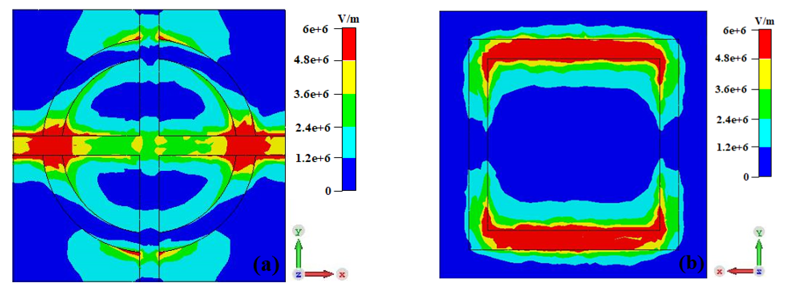
Figure 9 and
Figure 10 show the electric field distribution of metamaterial at 8 THz and 10 THz with silicon conductivity of 50,000 S/m. We can see that the electric field mainly concentrates on the left and right parts of the transverse resistive film at 8 THz and 10 THz. Obviously, the electric field distribution at the resonant frequency is similar to the coupling resonant characteristic of two electric dipoles, which indicates that the metamaterial produces electrical resonance at the action of incident wave [
28]. Due to the preventing transmission of the bottom metal ground plate, the electric field at the bottom metal ground plate is very low.
Figure 11 shows the electric field distribution of metamaterial at 5.12 THz with silicon conductivity of 150 S/m. We can see that the electric field also mainly concentrates on the left and right parts of the transverse resistive film at 5.12 THz. Obviously, the metamaterial also produces electric resonance at the action of incident wave [
28]. However, due to the frequency-selective surface of the bottom plate, the incident wave passes through the middle polyimide substrate and produces the symmetric electric field at the up and down parts of the bottom plate.
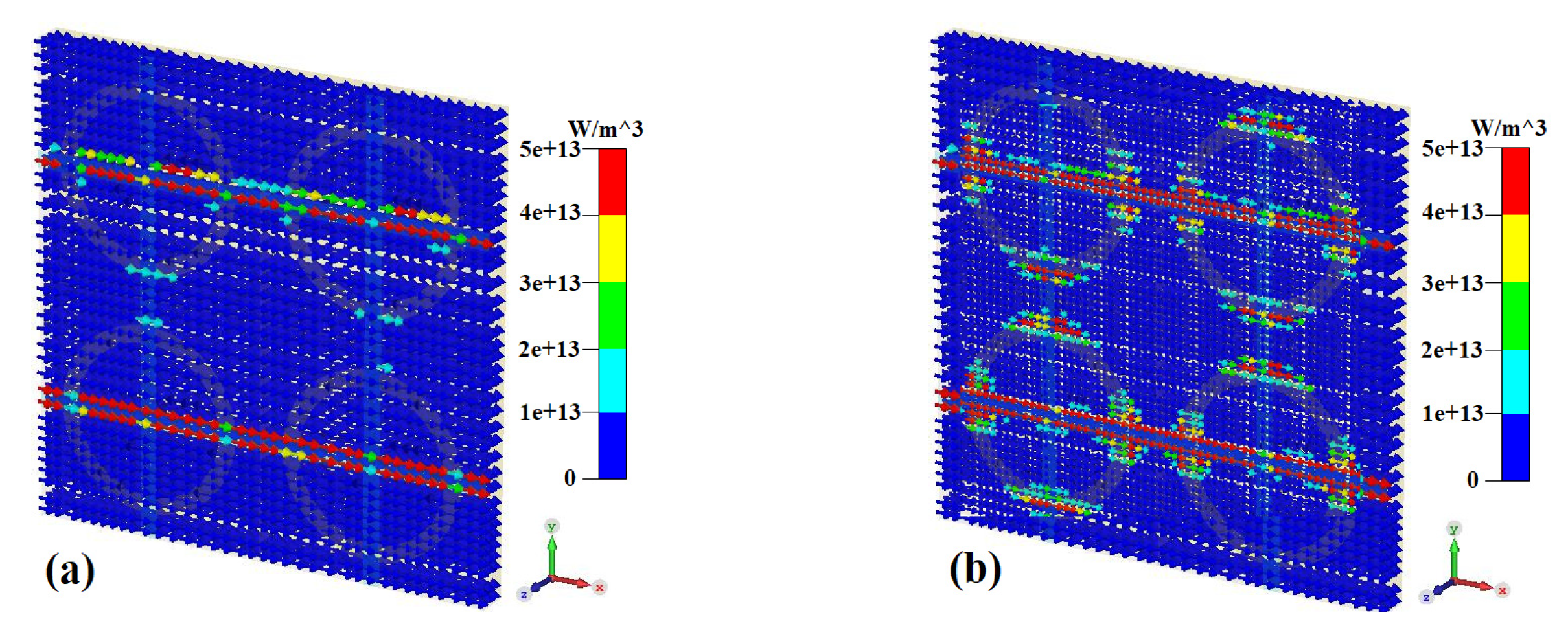
Figure 12 shows the power loss density distribution of the metamaterial at 8 THz and 10 THz when the conductivity of silicon is 50,000 S/m. We can see that the power loss mainly concentrates on the transverse resistive film, which is basically consistent with the electric field distribution. This indicates that the power loss of the metamaterial mainly originates from the ohm loss of the resistive film at the action of the incident wave. The ohm loss makes the metamaterial insensitive to frequency and can broaden the absorption bandwidth [
28].
Figure 13 shows the absorptivity (
S/m) of the metamaterial at different incident angles of the incident waves. It is seen that the absorptivity gradually decreases with the increase in the incident angle at TE mode, mainly due to the weakening of impedance matching between the metamaterial and free space [
29], but it maintains a high absorptivity within the range of 40°, and the absorptivity is basically unchanged at the range of 0° to 40° at TM mode.
Figure 14 displays the transmission coefficient (
S/m) of the metamaterial at different incident angles of the incident waves. One sees that the transmission coefficient gradually decreases with an increasing incident angle at both TE and TM modes.
To acquire a deeper insight into the physical principle, further parametric studies have been performed to analyze the metamaterial. As seen in
Figure 15, the absorptivity of the metamaterial gradually decreases with the increasing of the width
f when the conductivity of silicon is 50,000 S/m due to the increasing of the transmissivity at this time. However, the transmission coefficient gradually increases with the increasing of the width
f when the conductivity of silicon is 150 S/m. The transmission coefficient at 5.12 THz no longer noteworthily increases when the width
f increases to a certain program. The gold ground plane with square open slots can be equivalent to a parallel
LC circuit which is grounded. Its impedance can be expressed as
(
C is the equivalent capacitance of the open slots;
L is the equivalent inductance of the grid metal patch). The increase in the width
f can lead to the increase in the equivalent capacitance
C and then the impedance. This leads to fewer incident waves being grounded through the
LC parallel circuit, resulting in an increase in transmittance [
30]. However, it will no longer noteworthily increase when the equivalent capacitance increases to a certain program.
Figure 16 show the absorptivity of the metamaterial with the conductivity of silicon being 50,000 S/m at different structural size parameters of
c,
d, and
r. The bandwidth with the absorptivity of the metamaterial over 90% gradually increases with the increasing of structural size parameter
c. The main reason is that the increasing of structural size parameter
c can initiate the increasing of the resistance at the split of the gold ring and then cause the broadening of bandwidth according to Formula (4). The structural size parameter
d has almost no effect on the absorptivity of metamaterial. The absorptivity of the metamaterial gradually decreases with the increasing of the structural size parameter
r, mainly due to the weakening of impedance matching between the metamaterial and free space [
28].
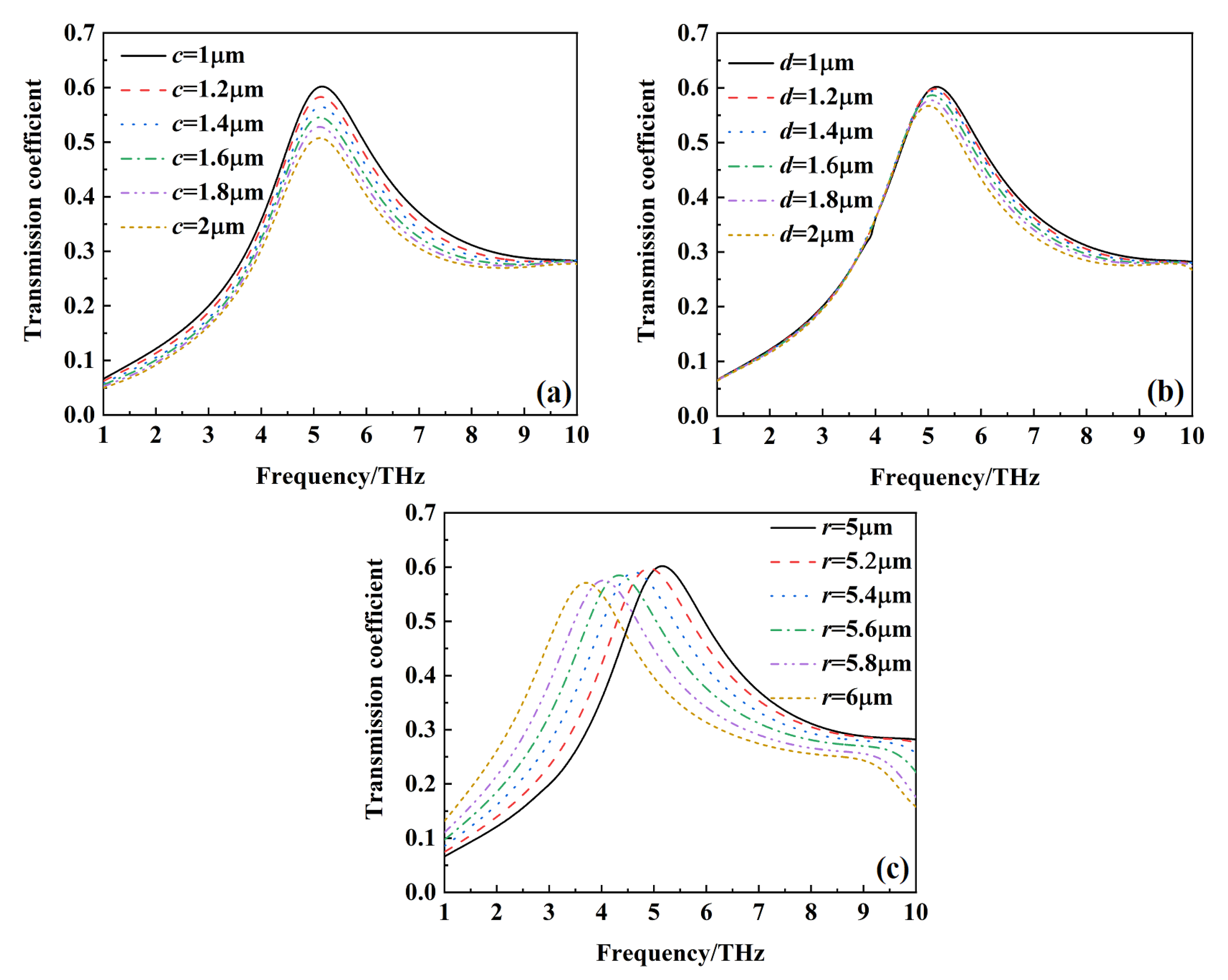
Figure 17 show the transmission of the metamaterial with the conductivity of silicon being 150 S/m at different structural size parameters of
c,
d, and
r. the increasing of the structural size parameter
c and
d prevent more incident wave transmission and then lead to the decreasing transmission of the metamaterial. The transmission frequency gradually shifts to a lower frequency with the increasing of the structural size parameter
r.
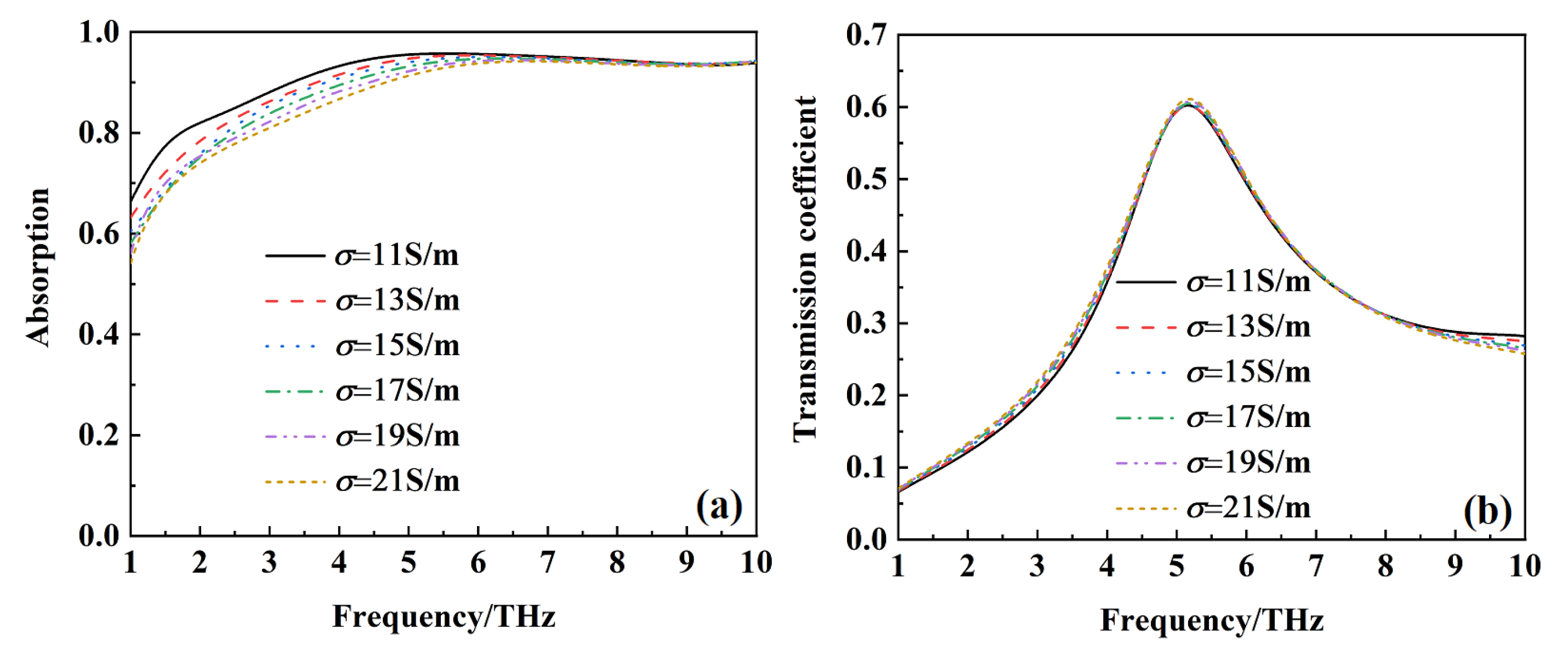
Figure 18 shows the absorptivity and the transmission of the metamaterial with a conductivity silicon of 50,000 S/m and 150 S/m at different conductivities of the resistive film. When the conductivity of silicon is 50,000 S/m, the increasing of the conductivity of the resistive film makes the bandwidth of the absorptivity over 90% gradually decrease, mainly due to the weaker impedance match of the metamaterial with free space. The transmission of the metamaterial is basically the same at different conductivities of the resistive film.

