ZnO-Based Materials: From Pauli’s Nonsense to a Key Enabling Technology

 , ,
, ,  ,
,  and
and 
Abstract
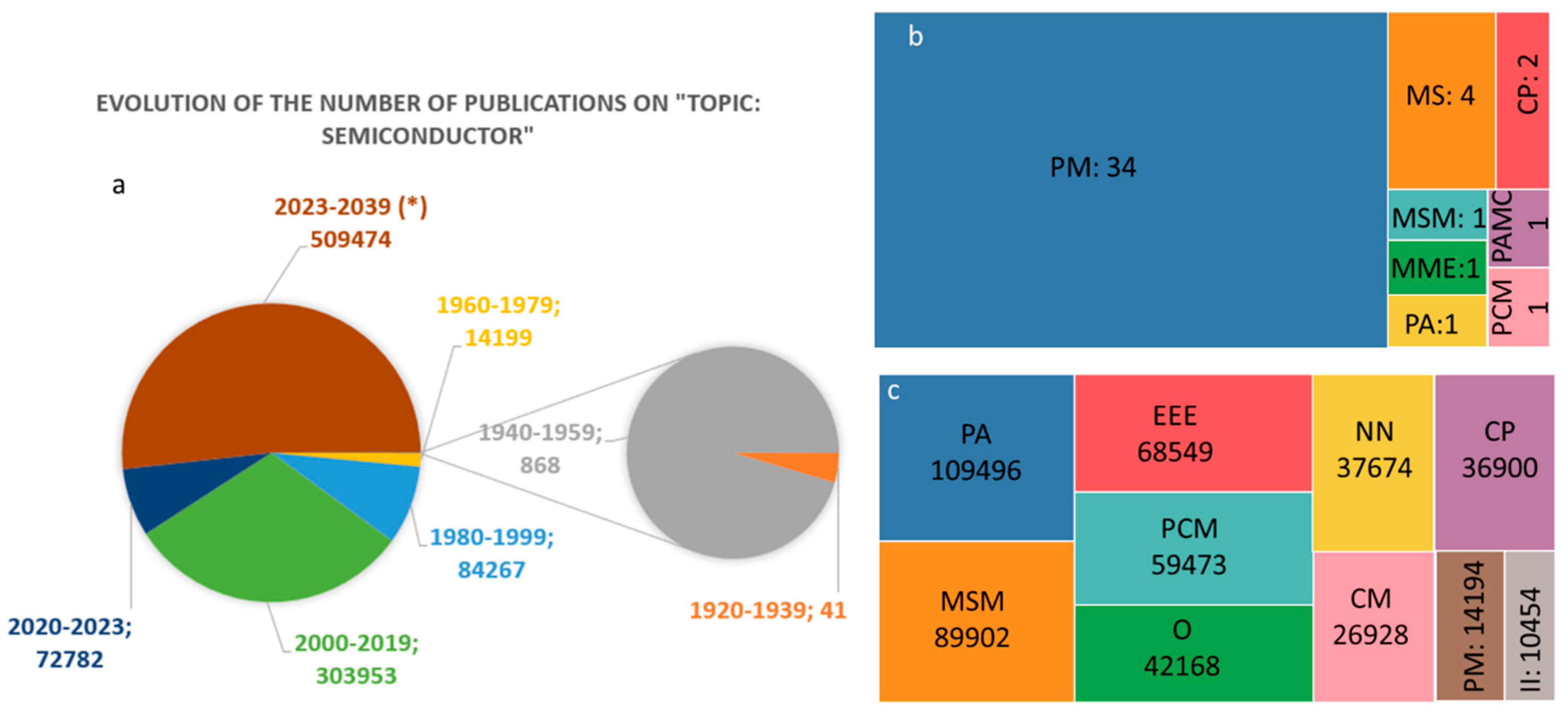
:1. Introduction
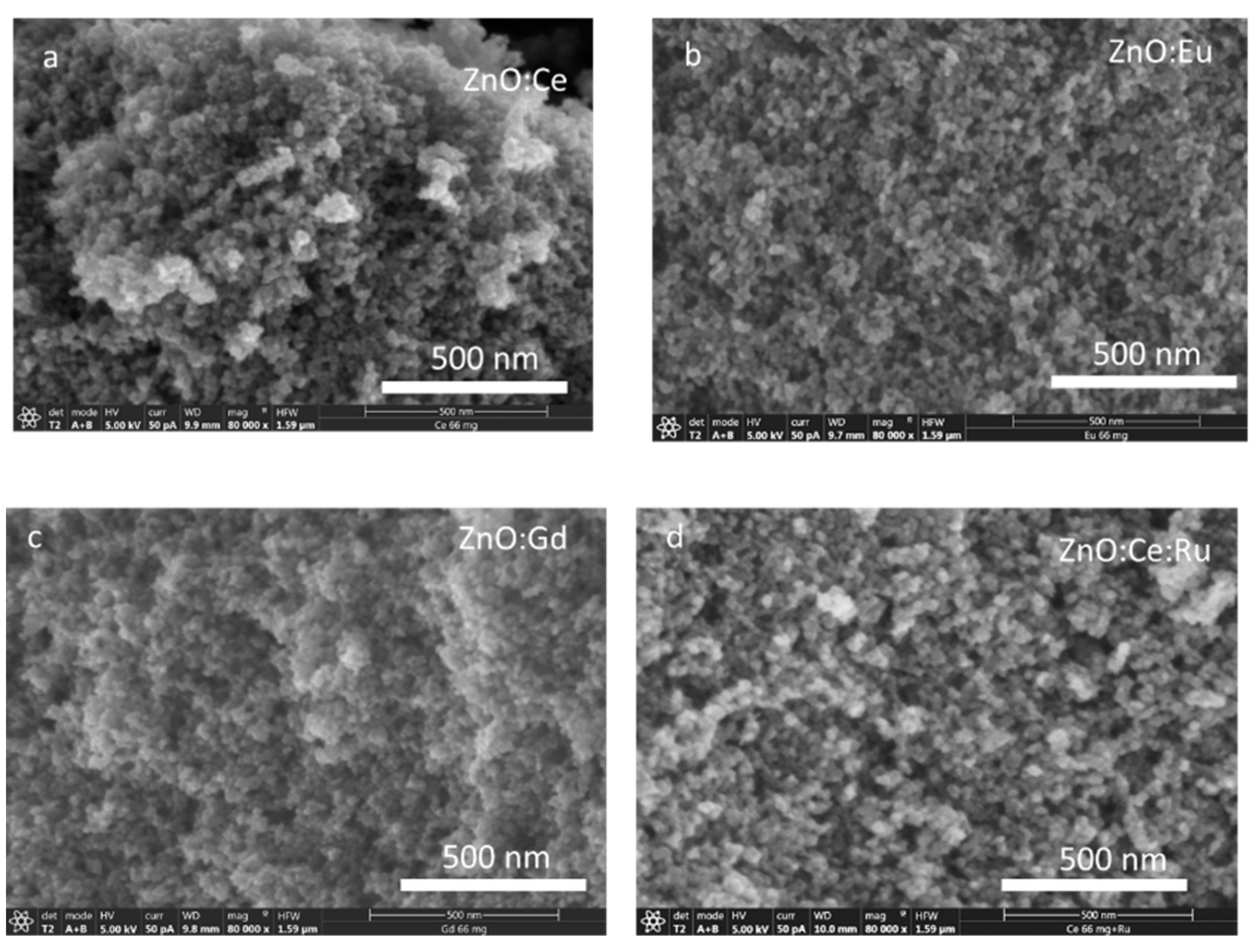
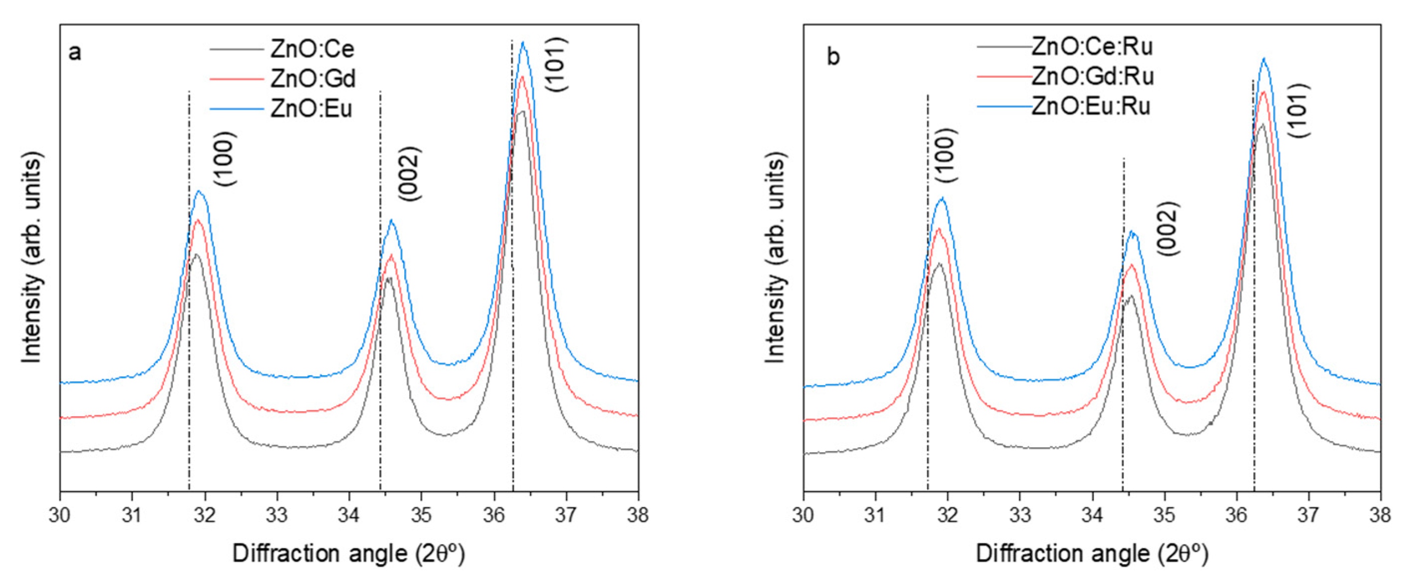
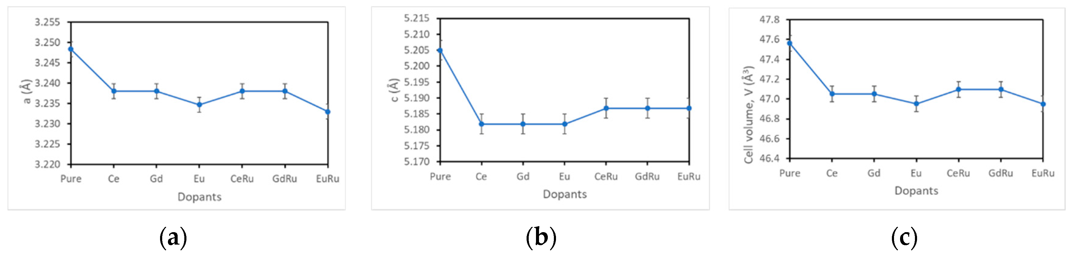
2. Experimental
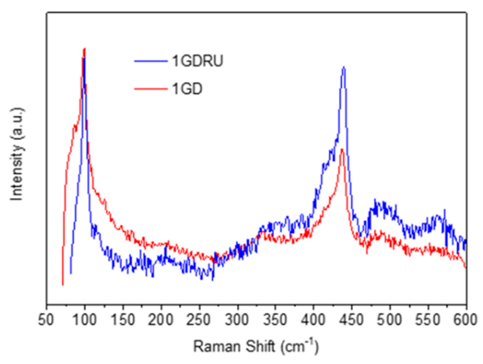
3. Results and Discussion
4. Conclusions
Supplementary Materials
Author Contributions
Funding
Institutional Review Board Statement
Informed Consent Statement
Data Availability Statement
Acknowledgments
Conflicts of Interest
References
- Zhu, L.; Zeng, W. Room-temperature gas sensing of ZnO-based gas sensor: A review. Sens. Actuators A Phys. 2017, 267, 242–261. [Google Scholar] [CrossRef]
- Yuan, S.; Duan, X.; Liu, J.; Ye, Y.; Lv, F.; Liu, T.; Zhang, X. Recent progress on transition metal oxides as advanced materials for energy conversion and storage. Energy Storage Mater. 2021, 42, 317–369. [Google Scholar] [CrossRef]
- Samadi, M.; Zirak, M.; Naseri, A.; Khorashadizade, E.; Moshfegh, A.Z. Recent progress on doped ZnO nanostructures for visible-light photocatalysis. Thin Solid Films 2016, 605, 2–19. [Google Scholar] [CrossRef]
- Tuller, H.L.; Bishop, S.R. Point Defects in Oxides: Tailoring Materials Through Defect Engineering. Annu. Rev. Mater. Res. 2011, 41, 369–398. [Google Scholar] [CrossRef]
- Nikolic, M.V.; Milovanovic, V.; Vasiljevic, Z.Z.; Stamenkovic, Z. Semiconductor Gas Sensors: Materials, Technology, Design, and Application. Sensors 2020, 20, 6694. [Google Scholar] [CrossRef] [PubMed]
- Monk, P.M.S.; Mortimer, R.J.; Rosseinsky, D.R. Metal Oxides. Electrochromism 1995, 10, 59–92. [Google Scholar] [CrossRef]
- Ong, C.B.; Ng, L.Y.; Mohammad, A.W. A review of ZnO nanoparticles as solar photocatalysts: Synthesis, mechanisms and applications. Renew. Sustain. Energy Rev. 2018, 81, 536–551. [Google Scholar] [CrossRef]
- Yu, X.; Marks, T.J.; Facchetti, A. Metal oxides for optoelectronic applications. Nat. Mater. 2016, 15, 383–396. [Google Scholar] [CrossRef]
- Wetchakun, K.; Samerjai, T.; Tamaekong, N.; Liewhiran, C.; Siriwong, C.; Kruefu, V.; Wisitsoraat, A.; Tuantranont, A.; Phanichphant, S. Semiconducting metal oxides as sensors for environmentally hazardous gases. Sens. Actuators B Chem. 2011, 160, 580–591. [Google Scholar] [CrossRef]
- Seshadri, R. Oxide Crystal Structures: The Basics. 2020. Available online: https://www.mrl.ucsb.edu/~seshadri/2015_218/OxidesStructures-BVS.pdf (accessed on 25 September 2023).
- Yoon, Y.; Truong, P.L.; Lee, D.; Ko, S.H. Metal-Oxide Nanomaterials Synthesis and Applications in Flexible and Wearable Sensors. ACS Nanosci. Au 2022, 2, 64–92. [Google Scholar] [CrossRef]
- Charles, V.L.P.; Crowther, W.H. Preparation and Properties of Zinc Oxide and Cadmium Oxide. J. Am. Chem. Soc. 1917, 39, 1046–1063. [Google Scholar]
- Haga, Y.; Haga, E. Ueber die Lumineszenz des Zinkoxyds. Phys. Z. 1922, 23, 98–104. [Google Scholar]
- Cooper, J.R.; Rhoderick, E.H. Copper-doped zinc oxide—A new room-temperature varistor. J. Phys. D Appl. Phys. 1967, 1, 493–496. [Google Scholar]
- Ozgür, Ü.; Alivov, Y.I.; Liu, C.; Teke, A.; Reshchikov, M.A.; Doğan, S.; Avrutin, V.; Cho, S.-J.; Morkoç, H. A comprehensive review of ZnO materials and devices. J. Appl. Phys. 2005, 98, 041301. [Google Scholar] [CrossRef]
- Kumari, P.; Misra, K.P.; Chattopadhyay, S.; Samanta, S. A brief review on transition metal ion doped ZnO nanoparticles and its optoelectronic applications. Mater. Today Proc. 2021, 43, 3297–3302. [Google Scholar] [CrossRef]
- Kumar, R.; Al-Dossary, O.; Kumar, G.; Umar, A. Zinc Oxide Nanostructures for NO2 Gas–Sensor Applications: A Review. Nano-Micro Lett. 2015, 7, 97–120. [Google Scholar] [CrossRef] [PubMed]
- Singh, P.; Kumar, R.; Singh, R.K. Progress on Transition Metal-Doped ZnO Nanoparticles and Its Application. Ind. Eng. Chem. Res. 2019, 58, 17130–17163. [Google Scholar] [CrossRef]
- Daksh, D.; Agrawal, Y.K. Rare Earth-Doped Zinc Oxide Nanostructures: A Review. Rev. Nanosci. Nanotechnol. 2016, 5, 1–27. [Google Scholar] [CrossRef]
- Kumar, S.G.; Kavitha, R.; Sushma, C. Doped zinc oxide nanomaterials: Structure–electronic properties and photocatalytic applications. 2020, 31, 285–312. Interface Sci. Technol. 2020, 31, 285–312. [Google Scholar] [CrossRef]
- Bhati, V.S.; Hojamberdiev, M.; Kumar, M. Enhanced sensing performance of ZnO nanostructures-based gas sensors: A review. Energy Rep. 2020, 6, 46–62. [Google Scholar] [CrossRef]
- Bong, H.-Y.; Umar, A. Metal Oxide Nanostructures and Their Applications; American Scientific Publishers: Valencia, CA, USA, 2010. [Google Scholar]
- Ahmad, M.; Zhu, J. ZnO based advanced functional nanostructures: Synthesis, properties and applications. J. Mater. Chem. 2011, 21, 599–614. [Google Scholar] [CrossRef]
- Wang, Z. Novel nanostructures of ZnO for nanoscale photonics, optoelectronics, piezoelectricity, and sensing. Appl. Phys. A 2007, 88, 7–15. [Google Scholar] [CrossRef]
- Kołodziejczak-Radzimska, A.; Jesionowski, T. Zinc Oxide—From Synthesis to Application: A Review. Materials 2014, 7, 2833–2881. [Google Scholar] [CrossRef] [PubMed]
- Skompska, M.; Zarębska, K. Electrodeposition of ZnO Nanorod Arrays on Transparent Conducting Substrates–a Review. Electrochim. Acta 2014, 127, 467–488. [Google Scholar] [CrossRef]
- Wang, Z.L. ZnO nanowire and nanobelt platform for nanotechnology. Mater. Sci. Eng. R Rep. 2009, 64, 33–71. [Google Scholar] [CrossRef]
- Ajmal, H.M.S.; Khan, F.; Huda, N.U.; Lee, S.; Nam, K.; Kim, H.Y.; Eom, T.-H.; Kim, S.D. High-Performance Flexible Ultraviolet Photodetectors with Ni/Cu-Codoped ZnO Nanorods Grown on PET Substrates. Nanomaterials 2019, 9, 1067. [Google Scholar] [CrossRef]
- Ajmal, H.M.S.; Khan, F.; Nam, K.; Kim, H.Y.; Kim, S.D. Ultraviolet Photodetection Based on High-Performance Co-Plus-Ni Doped ZnO Nanorods Grown by Hydrothermal Method on Transparent Plastic Substrate. Nanomaterials 2020, 10, 1225. [Google Scholar] [CrossRef]
- Ronning, C.; Gao, P.X.; Ding, Y.; Wang, Z.L.; Schwen, D. Manganese-doped ZnO nanobelts for spintronics. Appl. Phys. Lett. 2004, 84, 783–785. [Google Scholar] [CrossRef]
- Willander, M.; Nur, O.; Bano, N.; Sultana, K. Zinc oxide nanorod-based heterostructures on solid and soft substrates for white-light-emitting diode applications. New J. Phys. 2009, 11, 125020. [Google Scholar] [CrossRef]
- Willander, M.; Nur, O.; Sadaf, J.R.; Qadir, M.I.; Zaman, S.; Zainelabdin, A.; Bano, N.; Hussain, I. Luminescence from Zinc Oxide Nanostructures and Polymers and their Hybrid Devices. Materials 2010, 3, 2643–2667. [Google Scholar] [CrossRef]
- Singh, P.; Singh, R.K.; Kumar, R. Journey of ZnO quantum dots from undoped to rare-earth and transition metal-doped and their applications. RSC Adv. 2021, 11, 2512–2545. [Google Scholar] [CrossRef] [PubMed]
- Ariza, R.; Pavón, F.; Urbieta, A.; Fernández, P. Study of the influence of dopant precursor on the growth and properties of Li-doped ZnO. J. Phys. Chem. Solids 2020, 139, 109354. [Google Scholar] [CrossRef]
- Urbieta, A.; Fernández, P.; Piqueras, J. Nanowires and stacks of nanoplates of Mn doped ZnO synthesized by thermal evaporation-deposition. Mater. Chem. Phys. 2012, 132, 1119–1124. [Google Scholar] [CrossRef]
- Galli, G. Solid-state physics: Doping the undopable. Nature 2005, 436, 32–33. [Google Scholar] [CrossRef]
- Zhang, S.B.; Wei, S.-H.; Zunger, A. Microscopic Origin of the Phenomenological Equilibrium “Doping Limit Rule” in n-Type III-V Semiconductors. Phys. Rev. Lett. 2000, 84, 1232–1235. [Google Scholar] [CrossRef]
- Tang, K.; Gu, S.-L.; Ye, J.-D.; Zhu, S.-M.; Zhang, R.; Zheng, Y.-D. Recent progress of the native defects and p-type doping of zinc oxide. Chin. Phys. B 2017, 26, 047702. [Google Scholar] [CrossRef]
- Avrutin, V.; Silversmith, D.J.; Morkoç, H. Doping Asymmetry Problem in ZnO: Current Status and Outlook. Proc. IEEE 2010, 98, 1269–1280. [Google Scholar] [CrossRef]
- Yan, Y.; Wei, S.-H. Doping asymmetry in wide-bandgap semiconductors: Origins and solutions. Phys. Status Solidi (b) 2008, 245, 641–652. [Google Scholar] [CrossRef]
- Fan, J.; Sreekanth, K.; Xie, Z.; Chang, S.; Rao, K. p-Type ZnO materials: Theory, growth, properties and devices. Prog. Mater. Sci. 2013, 58, 874–985. [Google Scholar] [CrossRef]
- Pal, P.P.; Manam, J. Enhanced luminescence of ZnO:RE3+ (RE=Eu, Tb) nanorods by Li+ doping and calculations of kinetic parameters. J. Lumin. 2014, 145, 340–350. [Google Scholar] [CrossRef]
- Zhong, Tian and Philippe Goldner, Emerging rare-earth doped material platforms for quantum nanophotonics. Nanophotonics 2019, 8, 2003–2015. [CrossRef]
- Gaggero, E.; Calza, P.; Cerrato, E.; Paganini, M.C. Cerium-, Europium- and Erbium-Modified ZnO and ZrO 2 for Photocatalytic Water Treatment Applications: A Review. Catalysts 2021, 11, 1520. [Google Scholar] [CrossRef]
- Kumar, V.; Ntwaeaborwa, O.M.; Soga, T.; Dutta, V.; Swart, H.C. Rare Earth Doped Zinc Oxide Nanophosphor Powder: A Future Material for Solid State Lighting and Solar Cells. ACS Photon. 2017, 4, 2613–2637. [Google Scholar] [CrossRef]
- Ryu, Y.K.; Fernández, P.; Piqueras, J. Growth and characterization of Er-doped ZnO elongated nanostructures. Phys. Status Solidi (a) 2011, 208, 868–873. [Google Scholar] [CrossRef]
- Fan, R.; Lu, F.; Li, K. Single-mode channel waveguide at 1540 nm in Er-doped ZnO thin film. J. Lumin. 2017, 192, 410–413. [Google Scholar] [CrossRef]
- Lo, J.-W.; Lin, C.-A.; He, J.-H. Er-Doped ZnO Nanorod Arrays with Enhanced IR Emission by Using Au Island Films. Curr. Nanosci. 2011, 7, 282–287. [Google Scholar] [CrossRef]
- Kenyon, A. Recent developments in rare-earth doped materials for optoelectronics. Prog. Quantum Electron. 2002, 26, 225–284. [Google Scholar] [CrossRef]
- Zhou, Z.-Q.; Liu, C.; Li, C.-F.; Guo, G.-C.; Oblak, D.; Lei, M.; Faraon, A.; Mazzera, M.; de Riedmatten, H. Photonic Integrated Quantum Memory in Rare-Earth Doped Solids. Laser Photonics Rev. 2023, 2300257. [Google Scholar] [CrossRef]
- Eliseeva, S.V.; Bünzli, J.C. Lanthanide luminescence for functional materials and bio-sciences. Chem. Soc. Rev. 2010, 39, 1–380. [Google Scholar] [CrossRef]
- Singh, A.K.; Singh, S.K.; Rai, S.B. Role of Li+ion in the luminescence enhancement of lanthanide ions: Favorable modifications in host matrices. RSC Adv. 2014, 4, 27039–27061. [Google Scholar] [CrossRef]
- Krishna, R.; Haranath, D.; Singh, S.P.; Chander, H.; Pandey, A.C.; Kanjilal, D. Synthesis and improved photoluminescence of Eu:ZnO phosphor. J. Mater. Sci. 2007, 42, 10047–10051. [Google Scholar] [CrossRef]
- Khanum, R.; Das, N.M.; Moirangthem, R.S. Defect engineered ZnO whispering gallery modes via doping with alkali metal ions for label-free optical sensors. J. Appl. Phys. 2019, 125, 173107. [Google Scholar] [CrossRef]
- Ariza, R.; Sotillo, B.; Pavón, F.; Urbieta, A.; Fernández, P. Evolution of Whispering Gallery Modes in Li-Doped ZnO Hexagonal Micro- and Nanostructures. Appl. Sci. 2020, 10, 8602. [Google Scholar] [CrossRef]
- Pavón, F.; Urbieta, A.; Fernández, P. Luminescence and light guiding properties of Er and Li codoped ZnO nanostructures. J. Lumin. 2018, 195, 396–401. [Google Scholar] [CrossRef]
- Pavón, F.; Ariza, R.; Urbieta, A.; Fernández, P. Morphology, Luminescence, and Optical Properties of Tb- and Li-Codoped ZnO Elongated Nano- and Microstructures. Phys. Status Solidi (a) 2022, 219. [Google Scholar] [CrossRef]
- Cuscó, R.; Alarcón-Lladó, E.; Ibáñez, J.; Artús, L.; Jiménez, J.; Wang, B.; Callahan, M.J. Temperature dependence of Raman scattering in ZnO. Phys. Rev. B 2007, 75, 165202. [Google Scholar] [CrossRef]
- Vempati, S.; Mitra, J.; Dawson, P. One-step synthesis of ZnO nanosheets: A blue-white fluorophore. Nanoscale Res. Lett. 2012, 7, 470. [Google Scholar] [CrossRef]
- Kumar, V.; Prakash, J.; Pathak, D.; Sharma, D.P.; Purohit, L.P.; Swart, H.C. Ion beam engineering of implanted ZnO thin films for solar cell and lighting applications. Chem. Eng. J. Adv. 2023, 15, 100501. [Google Scholar] [CrossRef]
- Galdámez-Martinez, A.; Santana, G.; Güell, F.; Martínez-Alanis, P.R.; Dutt, A. Photoluminescence of ZnO Nanowires: A Review. Nanomaterials 2020, 10, 857. [Google Scholar] [CrossRef]


| Main Dopant (2% wt) | Codopant (0.25% wt) | Name |
|---|---|---|
| Ce | None | 1CE |
| Gd | 1GD | |
| Eu | 1EU | |
| Ce | Ru | 1CERU |
| Gd | 1GDRU | |
| Eu | 1EURU |
| Cation | Precursor | Supplier | CAS Number |
|---|---|---|---|
| Ce | Ce(CH3CO2)3•H2O | Sigma-Aldrich | 206996-60-3 |
| Gd | Gd(NO3)3•6H2O | Sigma-Aldrich | 19598-90-4 |
| Eu | Eu(NO3)3•5H2O | Sigma-Aldrich | 63026-01-7 |
| Ru | RuCl3•xH2O | Sigma-Aldrich | 14898-67-0 |
| Cation | Charge | Crystal Radius | Ionic Radius | |
|---|---|---|---|---|
| Host | Zn | 2 | 0.88 | 0.74 |
| TM | Ru | 3 | 0.82 | 0.68 |
| 4 | 0.76 | 0.62 | ||
| 5 | 0.705 | 0.565 | ||
| RE | Ce | 3 | 1.15 | 1.01 |
| 4 | 1.01 | 0.87 | ||
| Eu | 2 | 1.31 | 1.17 | |
| 3 | 1.087 | 0.947 | ||
| Gd | 3 | 1.078 | 0.938 |
Disclaimer/Publisher’s Note: The statements, opinions and data contained in all publications are solely those of the individual author(s) and contributor(s) and not of MDPI and/or the editor(s). MDPI and/or the editor(s) disclaim responsibility for any injury to people or property resulting from any ideas, methods, instructions or products referred to in the content. |
© 2023 by the authors. Licensee MDPI, Basel, Switzerland. This article is an open access article distributed under the terms and conditions of the Creative Commons Attribution (CC BY) license (https://creativecommons.org/licenses/by/4.0/).
Share and Cite
Ramos-Justicia, J.F.; Ferreiro, A.; Flores-Carrasco, G.; Rodríguez-Cañamero, S.; Urbieta, A.; Rabanal, M.E.; Fernández, P. ZnO-Based Materials: From Pauli’s Nonsense to a Key Enabling Technology. Photonics 2023, 10, 1106. https://doi.org/10.3390/photonics10101106
Ramos-Justicia JF, Ferreiro A, Flores-Carrasco G, Rodríguez-Cañamero S, Urbieta A, Rabanal ME, Fernández P. ZnO-Based Materials: From Pauli’s Nonsense to a Key Enabling Technology. Photonics. 2023; 10(10):1106. https://doi.org/10.3390/photonics10101106
Chicago/Turabian StyleRamos-Justicia, Juan Francisco, Adalyz Ferreiro, Gregorio Flores-Carrasco, Sara Rodríguez-Cañamero, Ana Urbieta, María Eugenia Rabanal, and Paloma Fernández. 2023. "ZnO-Based Materials: From Pauli’s Nonsense to a Key Enabling Technology" Photonics 10, no. 10: 1106. https://doi.org/10.3390/photonics10101106
APA StyleRamos-Justicia, J. F., Ferreiro, A., Flores-Carrasco, G., Rodríguez-Cañamero, S., Urbieta, A., Rabanal, M. E., & Fernández, P. (2023). ZnO-Based Materials: From Pauli’s Nonsense to a Key Enabling Technology. Photonics, 10(10), 1106. https://doi.org/10.3390/photonics10101106