1. Introduction
GaN semiconductor devices can implement higher-frequency operation than conventional Si-based semiconductor devices because two-dimensional electron gas (2DEG) can be formed inside GaN semiconductor devices. Two-dimensional electron gas has high electron mobility, which accelerates electronic conduction in lateral GaN semiconductor devices. Because of the epitaxial growth of GaN layers on Si, SiC, or sapphire substrates, the electric field occurs on the surface of a lateral active layer. Therefore, laterally configured GaN semiconductor devices can withstand a rating voltage of <650 V; however, a new cascode GaN-FET (field-effect transistor) raised the withstand voltage to 900 V [
1,
2].
“Laser” is a word formed from the initial letters of “light amplification by stimulated emission of radiation”. According to the various materials used for configuration, lasers can be classified as semiconductor lasers, fiber lasers, gas lasers, or solid-state lasers.
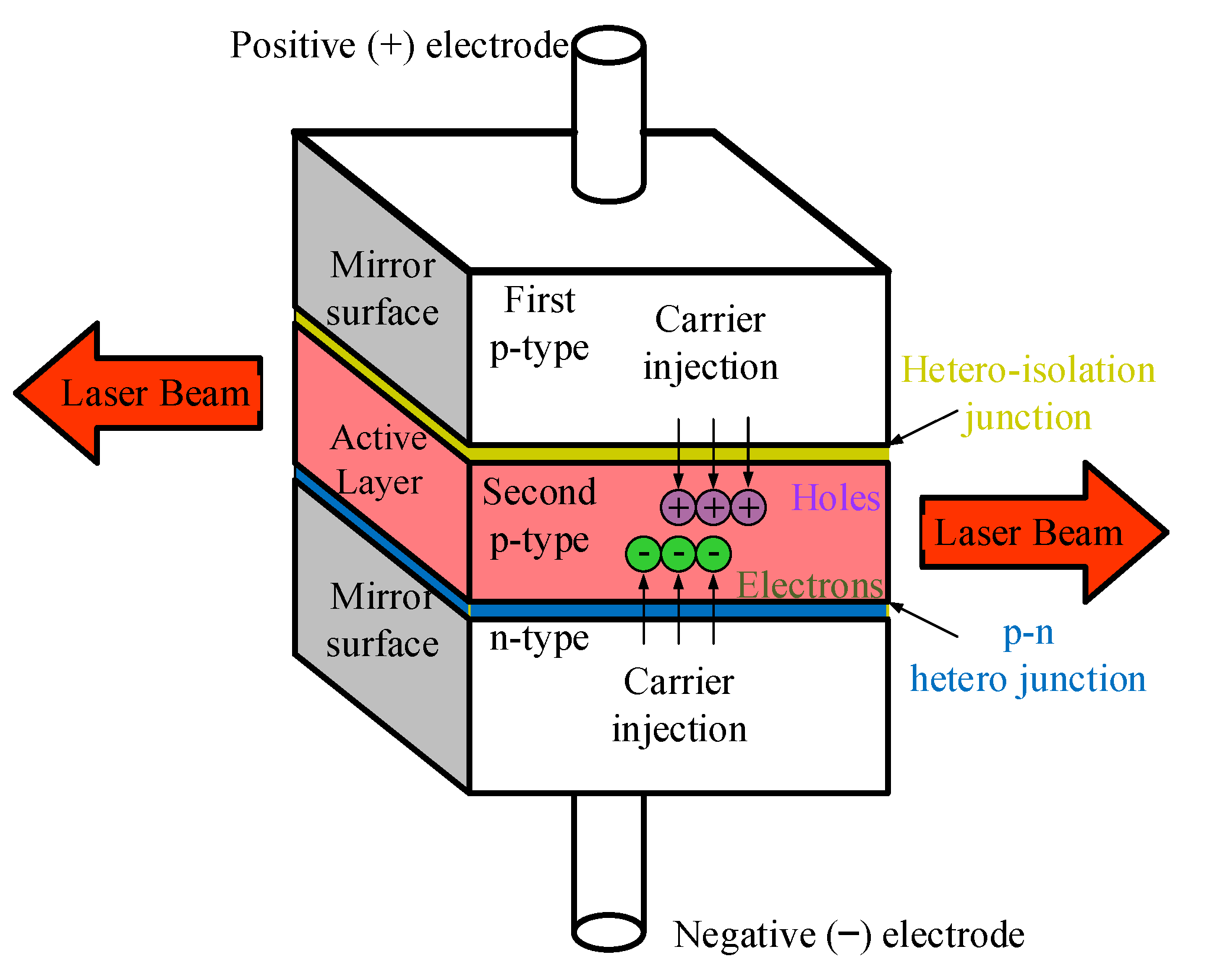
Figure 1 illustrates a simple semiconductor laser configuration. In
Figure 1, the active layer of the laser semiconductor is the second p-type semiconductor, which is placed in between the first p-type and n-type semiconductors. The first p-type semiconductor can be regarded as the positive (+) electrode, while the bottom of the n-type semiconductor can be regarded as the negative (−) electrode. When the positive/negative electrodes apply the electric field, the active layer can be excited to emit a stream of light that can be amplified by mirror surfaces to enhance emitting a laser beam [
3]. When a power source is applied to the positive/negative electrodes and the laser semiconductor is in forward-bias operation, the electrons from the n-type semiconductor are injected into the second p-type semiconductor, and the wide bandgap of the heteroisolation junction between the first and second p-type semiconductors can restrict the amount of electron compounding in the active layer; as a result of the carrier confinement, the population inversion probabilities can be increased to promote high-intensity light emission [
4].
Semiconductor lasers are equipped with several excellent characteristics, such as monochromaticity, high directionality, high coherence, and high energy density. Diode lasers with wavelengths of 635 nm have been applied to noncontact treatments such as photodynamic therapy groups for toluidine blue and the stability of orthodontic mini-implants [
5,
6].
Table 1 lists relevant studies on optoelectronic semiconductors with linear regulators. In the literature [
7,
8,
9,
10], light-emitting diodes (LEDs) were typically used as the light source, and bipolar junction transistors (BJT) and metal-oxide-semiconductor field-effect transistors (MOSFET) were used as the linear regulators. Only in [
11] was a GaN HEMT used. In addition, in [
11], a dimming function was implemented using pulse-width modulation (PWM) with a frequency of <2 kHz.
Optical output power adjustment for a laser diode (LD) is similar to illumination dimming for LEDs. Therefore, in this study, high-frequency PWM and constant-current modes were implemented to adjust the optical output power of a laser diode; the PWM frequency was adjustable to 200 kHz, while the minimum short-pulsed time was 2 µs to reach the maximum operating current.
LEDs associated with GaN materials have many benefits, such as high luminous efficiency, low energy consumption, long operation lifetime, and broad spectral range. Hence, GaN-based LEDs have been applied usefully in disinfection, automotive front lighting, solid-state lighting, and full-color displays [
12,
13,
14,
15]. Moreover, combinations of GaN devices and laser diodes have been used in a few practical applications, such as photoconductive semiconductor switches, light detection and ranging (LIDAR) systems, and plasma-assisted molecular beam epitaxy systems [
16,
17,
18].
2. Equivalent Circuits of Laser Diode and GaN HEMT
2.1. Laser Diode
A laser diode with a wavelength of 635 nm (model number: HL63193MG, Oclaro Inc., San Jose, CA, United States) was used in this study, the specifications of which are listed in
Table 2 [
19].
The physical configuration and equivalent circuit (EC) of the laser diode are illustrated in
Figure 2. In
Figure 2a, T
ld1 and T
ld2 are the metal terminals. The outside of the physical configuration could connect with the power source to drive the laser chip. The inside of the physical configuration here included the p-contact, n-contact, bonding wires, active layer, and substrate.
In
Figure 2b, the equivalent circuit of the laser diode is depicted. It had package and chip parasitic components. The package parasitic components included the bonding wire resistance
Rpld, bonding wire inductance
Lpld, and extracted submount capacitance
Cpld. The chip parasitic components included the intrinsic diode
Dcld, chip resistance
Rcld, and chip electrode capacitance
Ccld [
20,
21]; the diode property is presented using
Dcld.
2.2. GaN HEMT
The GaN HEMT device used was a GS61004B (GaN Systems Inc., Ottawa, ON, Canada);
Table 3 lists its specifications.
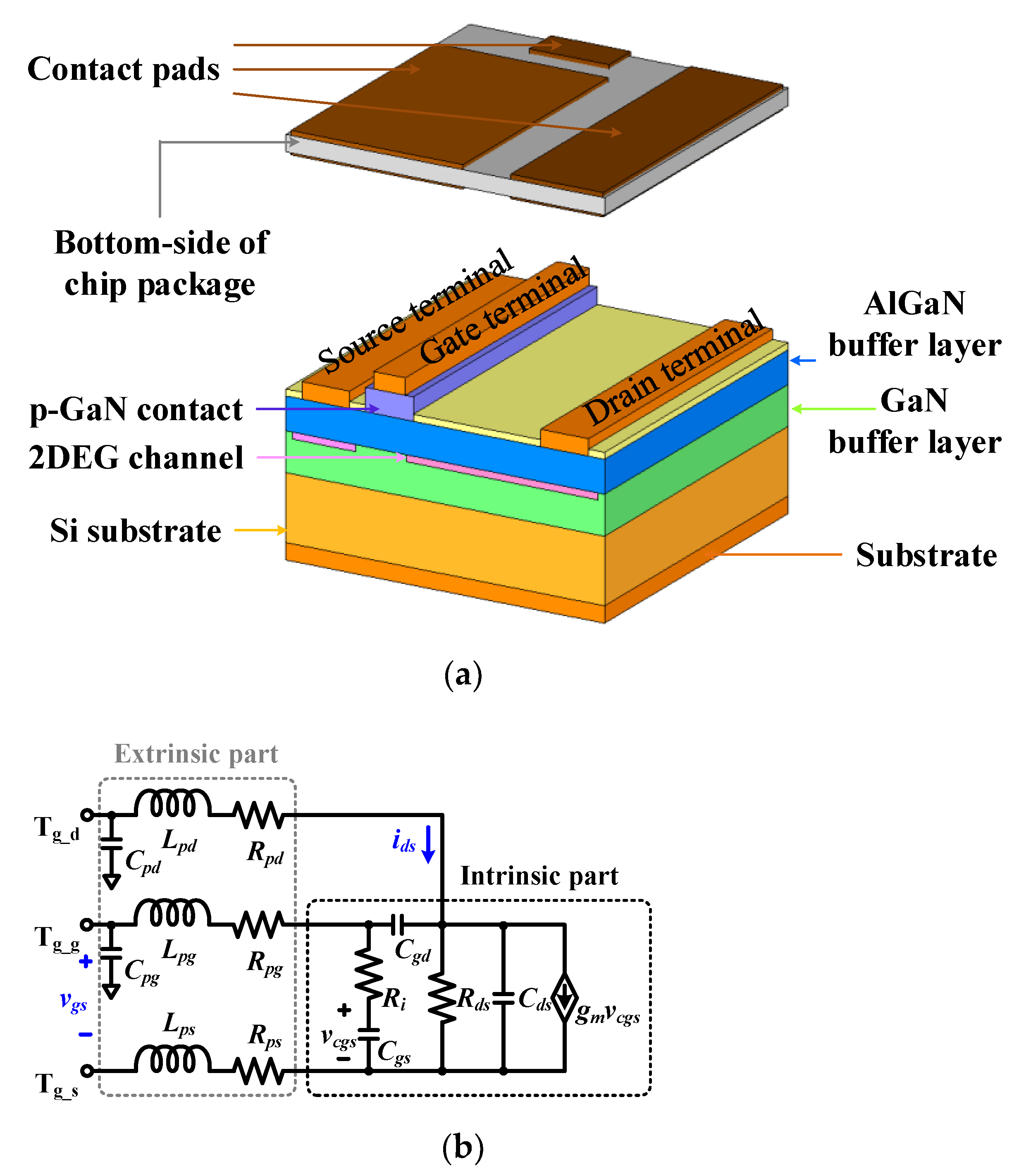
The physical configuration and equivalent circuit of the GaN HEMT are illustrated in
Figure 3. A particular package (flat no-lead package) was developed and used for the GaN HEMT from the design of GaN Systems Inc; using this physical package, the intrinsic parasitic inductance was reduced.
Figure 3a illustrates the physical package configuration, and
Figure 3b is the GaN HEMT equivalent circuit. The electrical components included a substrate, Si substrate, GaN buffer layer, two-dimensional electron gas channel, AlGaN buffer layer, p-GaN contact, gate, drain, source electrodes, the bottom of the chip package, and contact pads [
22,
23].
The equivalent circuit of the GaN HEMT had intrinsic and extrinsic parts, as shown in
Figure 3b [
24,
25,
26,
27]. The intrinsic part components included the resistances (
Rgs and
Rds), capacitance (
Cds), and dependent current source (
gmvg);
gm is the transconductance value, and
vg is the across voltage on
Cgs. The extrinsic part components include the inductances (
Lpd,
Lpg, and
Lps), capacitances (
Cpd and
Cpg), and resistances (
Rpd,
Rpg, and
Rps).
Because of the air–bridge source connection, the pad connection, electrode, and cross capacitance formed the Cpd and Cpg. The parasitic resistances (Rpd, Rpg, and Rps) represent the contact resistance and semiconductor bulk resistance on the drain, gate, and source terminals. The parasitic inductances (Lpd, Lpg, and Lps) are at the GaN HEMT with contact pads on the bottom of the chip packages.
The gate electrode and drain-source channel formed the parallel-plate capacitance Cgs. The drain and source electrodes were installed along the two-dimensional electron gas channel, which formed Cds and Cgd. Rds is a channel resistance between the drain and source terminals.
3. Dynamic Operational Linear Regulator
Figure 4 is the circuit block diagram of the DOLR based on the GaN HEMT controlling the 635 nm-wavelength laser diode. The DOLR included the operational amplifier (OP), current buffer, GaN HEMT, current detection resistance (
Rcs), and the differential amplifier. The control circuit of the DOLR included the microcontroller unit (MCU), voltage buffer, integral circuit, GaN HEMT off switch (GHOS), and GHOS driver; the three laser diodes (L
a1, L
a2, and L
a3) could be controlled by the DOLR.
PWM ports 1 and 2 of the MCU output two signals (Vpwm1 and Vpwm2). The integral circuit could transfer the PWM voltage Vpwm2 to become a direct-current (DC) voltage. Via the voltage buffer preventing the loading effect, that DC voltage can be regarded as a reference voltage Viref for stabilizing the laser diode operating current Irld. The OP could compare the differential amplifier output voltage (Vda) with Viref to control the GaN HEMT. In order to enhance the driving ability of the OP output for Vop, the current buffer was used for the GaN HEMT turning-on operation. Then, the operating current of La1 to La3 could be controlled by the DOLR.
The drain–source channel resistance of the GaN HEMT could be regulated by the DOLR to control the drain terminal current. In addition, a short-pulsed current can be fulfilled from a high-frequency’s Vpwm1. Therefore, the high-bandwidth component must be used for the differential amplifier and current buffer.
The driving ability of Vpwm1 could be enhanced by the GHOS driver, as Vpwm1 synchronizing with Vghos could control the GHOS turning on/off to further manipulate the GaN HEMT. When Vghos was at the high-voltage level, the GHOS was turned on; then, the gate terminal of the GaN HEMT would become the low-voltage level, which is less than the threshold voltage, resulting in the GaN HEMT turning off. When Vghos was the low-voltage level, the GHOS could be turned off; then, the gate terminal of the GaN HEMT would become a high-voltage level, because the OP output voltage Vop through the current buffer could control the GaN HEMT. Meanwhile, the DOLR could be controlled to regulate Irld.
3.2. DOLR Specification
The DOLR’s specifications are listed in
Table 5.
3.3. Simulation Circuit
The circuit simulation software POWERSIM (Powersim Inc., Rockville, MD, United States) was used. Based on
Figure 4 and considering the parasitic components, the circuit block diagram of the simulation circuit is illustrated in
Figure 5.
Figure 5 depicts the parasitic components from the printed circuit board and power source.
Lpcb1,
Lpcb2,
Lpcb3, and
Lpcb4 are the parasitic wire inductances;
Rpcb1,
Rpcb2,
Rpcb3, and
Rpcb3 are parasitic wire resistances;
Lpcb1 and
Rpcb1 are on the printed circuit board between T
g_g and the current buffer;
Lpcb2 and
Rpcb2 are on the printed circuit board between T
g_g and the GHOS;
Lpcb3 and
Rpcb3 are on the printed circuit board between T
g_s and
Rcs; and
Lpcb4 and
Rpcb4 are on the printed circuit board between T
g_d and the third laser diode equivalent circuit of the cathode terminal T
k3.
The parasitic wire inductance and resistance on the power cable of the DOLR supply power (Vsp) were also considered. The parasitic wire inductance and resistance on the printed circuit board are Lpw and Rpw, respectively; the parasitic inductance from the Vsp is the Lpp. Lpw, Rpw, and Lpp were connected in series between Vsp and the anode terminal (Ta1) of the first laser diode equivalent circuit.
3.4. Parameter Considerations and Calculations for GaN HEMT
Because the physical package of the GaN HEMT (GS61004B) used a new preplated Au configuration rather than the conventional bonding wire, the parasitic inductances between the three electrodes (gate, source, and drain) and contact pads [
28,
29] were reduced. From [
29,
30], these parameter values were referenced, including
Lpd = 1.3 nH,
Lpg = 1.2 nH, and
Lps = 0.45 nH; moreover,
Rpd =
Rpg =
Rps = 1 mΩ was assumed. According to the GS61004B specification list in
Table 3,
Rgs = 0.9 Ω,
Rds = 27 mΩ,
Cgs = 295 pF,
Cgd = 6.2 pF, and
Cds = 133.8 pF.
The parameter
gm was the rate of change from the drain-to-source current
ids (
Figure 3b) and gate-to-source voltage
Vgs [
31,
32].
gm was calculated and expressed as
From the GS61004B datasheet [
22], the
ids and
vgs values were found on the device’s characteristic curve; therefore, both (4 V, 61 A) and (3 V, 39 A) could be substituted into (1) to obtain
gm = 22 S.
From [
17,
18],
Cpd and
Cpg were tiny, at approximately 10
−15 F; therefore, this study assumed
Cpd =
Cpg = 1 pF.
3.5. Parasitic Components on Printed Circuit Board
In this study, the copper wire on the printed circuit board was regarded as a rectangular conductor to evaluate the resistance and inductance values. From [
33], the inductance of a rectangular conductor can be calculated and expressed as
where
l,
w, and
h, represent the length, width, and thickness of the rectangular conductor, respectively. The length, width, and thickness units are millimeters (mm); the inductance
Lpcb unit is the microhenry (μH). In this paper, the copper conductor thickness was 0.035 mm. Moreover, the parasitic resistance of the copper conductor on the printed circuit board can be calculated and expressed as
where ξ represents the resistivity (in the present study, ξ = 1.73 × 10
−5 Ω-mm at 20 °C) and
A is the cross-sectional area of the copper conductor (
A =
w ×
h).
In the GaN HEMT turning-on loop (
Figure 5), the parasitic components on the printed circuit board were
Lpcb1 and
Rpcb1. In the GaN HEMT turning-off loop, the parasitic components on the printed circuit board were
Lpcb2 and
Rpcb2. Because the copper wire in the GaN HEMT turning-on loop had a length of 49.5 mm and a width of 1.5 mm, substituting the length = 49.5 mm and the width = 1.5 mm into (2) and (3) led to
Rpcb1 = 16 mΩ and
Lpcb1 = 46.2 nH. Moreover, because the copper wire in the GaN HEMT turning-off loop had a length of 42 mm and a width of 1.5 mm, substituting the length = 42 mm and the width = 1.5 mm into (2) and (3) led to
Rpcb2 = 13.2 mΩ and
Lpcb2 = 37.5 nH.
A copper wire between Tg_s and Rcs on the printed circuit board had a length of 27.3 mm and a width of 5.5 mm; substituting the length = 27.3 mm and width = 5.5 mm into (2) and (3) led to Lpcb3 = 15.9 nH and Rpcb3 = 2.5 mΩ. Moreover, the practical Rcs was 100 mΩ.
The copper wire between the Tg_d and the third laser diode equivalent circuit on the printed circuit board had a length of 1 mm and a width of 1 mm; substituting length = 1 mm and width = 1 mm into (2) and (3) led to Lpcb4 = 8.9 nH and Rpcb4 = 6.1 mΩ.
The power wire was connected to the first laser diode equivalent circuit with
Vcc. Because the power wire can be regarded as a cylindrical conductor, according to [
33,
34], its parasitic inductance can be calculated and expressed as
where
lw and
d represent the length and diameter of the power wire (cm);
β represents the relative permeability of copper (
β was set to 1 in this paper), and the units of
Lpw are nanohenries (nH). In this study, the power wire had
lw = 20 cm and
d = 0.2 cm; substituting
lw = 20 cm and
d = 0.2 cm into (3) and (4),
Lpw = 209.9 nH and
Rpw = 2.7 mΩ can be obtained. Moreover, the parasitic inductance
Lpp inside
Vcc was also considered, and
Lpp was set as 1.2 μH.
4. Circuit Simulation and Experiment
The simulation circuit using the PSIM is shown in
Figure 6. The simulation results are presented in
Figure 7. In
Figure 7,
Vpwm1 is the GHOS operating signal,
Viref is the reference voltage for the constant-current operation,
Vgs is the gate-to-source voltage of the GaN HEMT, and
Irld is the operating current for the three laser diodes.
In the present study,
Vpwm1 was zero, which represented no PWM signal. When
Viref was 0.4 V, the
Vgs of the DOLR could be controlled to regulate
Irld and maintain it at 0.4 A, as shown in
Figure 7a. When
Viref was 0.8 V, the
Vgs of the DOLR could be controlled to regulate
Irld and maintain it at 0.8 A, as shown in
Figure 7b.
Figure 7 displays results for a simulation of the constant-current mode operation of the DOLR.
Figure 8 shows results for the simulation the PWM-mode operation of the DOLR. The frequency of
Vpwm1 was 200 kHz,
Viref was 0.8 V, and
Irld spent 2.2 µs rising to the rated operating current at 0.8 A. In
Figure 8a–c, the short-pulsed times of
Irld were 2.25, 3, and 4 µs, respectively.
In accordance with
Figure 4, critical experimental waveforms are presented in
Figure 9and
Figure 10, including
Vpwm1,
Viref,
Vgs, and
Irld.
In the experimental waveform shown in
Figure 9a, when the microcontroller unit stopped outputting the PWM signal from the PWM port 1,
Vpwm1 was a low voltage level. When
Viref was set at 0.4 V,
Vgs could be regulated to control the GaN HEMT; hence,
Irld was operated in the constant current of 0.4 A. In the experimental waveform shown in
Figure 9b,
Vpwm1 was also at a low voltage level; however,
Viref was set at 0.8 V,
Vgs could be regulated to control the GaN HEMT, and
Irld could be operated in the constant current of 0.8 A.
In the experimental waveform shown in
Figure 10, the PWM mode was implemented for the laser diodes.
Irld could be operated in different PWMs. Because the microcontroller unit outputted the PWM signal from the PWM port 1,
Vpwm1 became a pulse signal, and both
Vgs and
Irld followed the change of
Vpwm1.
Viref was set at 0.8 V, and the rising time of
Irld was 2 µs to reach the maximum operating 0.8 A. In
Figure 10a–c, the duty cycle ratios of the PWMs were 40% (2 µs/5 µs), 60% (3 µs/5 µs), and 80% (4 µs/5 µs), respectively.
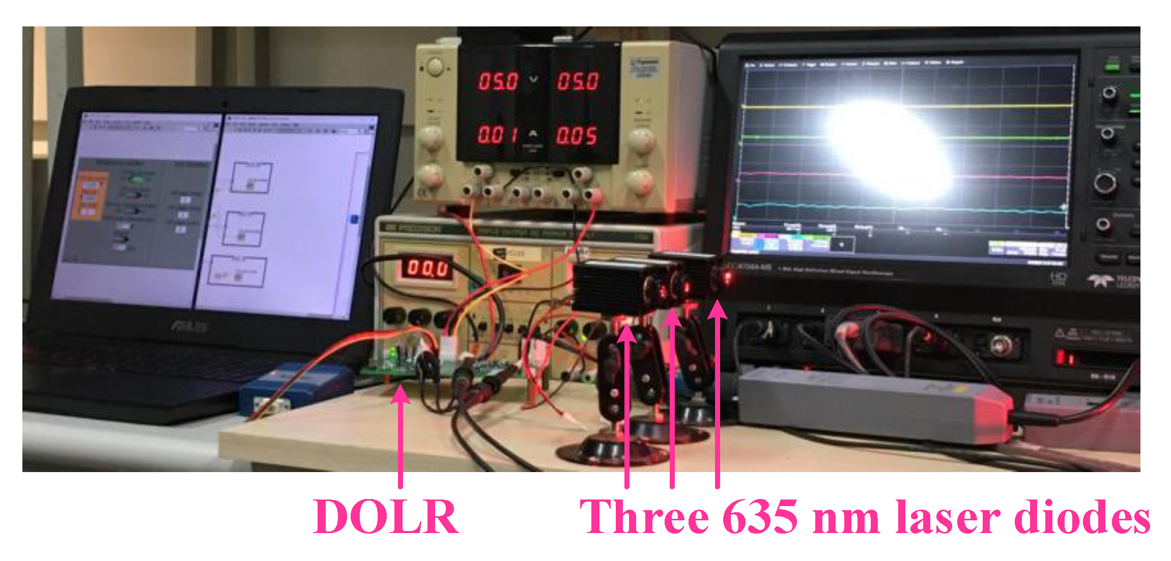
The DOLR prototype driving the three 635 nm laser diodes is shown in
Figure 11.
5. Conclusions
In this study, a GaN HEMT was incorporated with wide-bandwidth operational amplifiers to achieve a DOLR. Three 635 nm laser diodes were controlled by the DOLR; therefore, the laser diodes could be operated in the PWM mode to achieve a short-pulsed laser or in the constant-current mode to achieve a continuous-wave laser. In order to understand the operating current changes in laser diodes, this study used the equivalent circuits of the laser diode and GaN HEMT to simulate DOLR operations and observe the critical waveforms. From the simulations and experimental results, it was concluded that the operating current of the laser diode was influenced by critical factors including the device parasitic components and PCB layout. Using the developed DOLR prototype, three 635 nm laser diodes were controlled to achieve short-pulsed and continuous-wave lasers.
Author Contributions
Conceptualization, K.-J.P. and C.-H.L.; Methodology, K.-J.P.; Validation, K.-J.P.; Formal Analysis, K.-J.P.; Investigation, K.-J.P.; Writing—Original Draft Preparation, K.-J.P.; Writing—Review and Editing, K.-J.P. and C.-H.L.; Supervision, K.-J.P.; Project Administration, K.-J.P. All authors have read and agreed to the published version of the manuscript.
Funding
This research was funded by the Ministry of Science and Technology, Taiwan (grant numbers: MOST 110–2221–E–003–007, MOST 110-2221-E-011-081, and MOST 108–2221–E–003–028–MY2).
Institutional Review Board Statement
Not applicable.
Informed Consent Statement
Not applicable.
Data Availability Statement
All relevant data presented in the article are stored according to institutional requirements and, as such, are not available online. However, all data used in this Manuscript can be made available upon request to the authors.
Acknowledgments
The authors acknowledge the Ministry of Science and Technology, Taiwan, for supplying a research fund. Moreover, this article was subsidized by the National Taiwan Normal University (NTNU), Taiwan. Furthermore, the authors sincerely appreciate the great support from the Taiwan Building 302 Technology Center from the Featured Areas Research Center Program within the framework of the 303 Higher Education Sprout Project by the Ministry of Education in Taiwan.
Conflicts of Interest
The authors declare no conflict of interest.
References
- Xu, J.; Gu, L.; Ye, Z.; Kargarrazi, S.; Rivas-Davila, J. Cascode GaN/SiC: A wide-bandgap heterogenous power device for high-frequency applications. IEEE Trans. Power Electron. 2020, 35, 6340–6349. [Google Scholar] [CrossRef]
- Lyu, G.; Wang, Y.; Wei, J.; Zheng, Z.; Sun, J.; Zhang, L.; Chen, K. A normally-off copackaged SiC-JFET/GaN-HEMT cascode device for high-voltage and high-frequency applications. IEEE Trans. Power Elect. 2020, 35, 9669–9679. [Google Scholar] [CrossRef]
- Keyence Inc. Laser Technical Guide; Application Note of Keyence Inc.: Itasca, IL, USA, 2015. [Google Scholar]
- USHIO Inc. Chip Structure and Lasing Modes; USHIO Opto Semiconductor: Tokyo, Japan, 2014. [Google Scholar]
- Flieger, R.; Gedrange, T.; Grzech-Le’sniak, K.; Dominiak, M.; Matys, J. Low-level laser therapy with a 635 nm diode laser affects orthodontic mini-implants stability: A randomized clinical split-mouth trial. J. Clin. Med. 2020, 9, 112. [Google Scholar] [CrossRef] [PubMed] [Green Version]
- Tenore, G.; Palaia, G.; Migliau, G.; Mohsen, A.; Rocchetti, F.; Gaimari, G.; Impellizzeri, A.; Salapata, Y.; Berlutti, F.; Polimeni, A.; et al. Evaluation of photodynamic therapy using a diode laser 635 nm as an adjunct to conventional chemo-mechanical endodontic procedures against enterococcus faecalis biofilm: Ex-vivo study. Appl. Sci. 2020, 10, 2925. [Google Scholar] [CrossRef]
- Lohaus, L.; Rossius, A.; Dietrich, S.; Wunderlich, R.; Heinen, S. A dimmable LED driver with resistive DAC feedback control for adaptive voltage regulation. IEEE Trans. Ind. Appl. 2015, 51, 3254–3262. [Google Scholar] [CrossRef]
- Liu, P.; Hsu, Y.; Hsu, S. Drain-voltage balance and phase-shifted PWM control schemes for high-efficiency parallel-string dimmable LED drivers. IEEE Trans. Ind. Electron. 2018, 65, 6168–6176. [Google Scholar] [CrossRef]
- Meraj, M.; Rahman, S.; Iqbal, A.; Ben-Brahim, L. High brightness and high voltage dimmable LED driver for advanced lighting system. IEEE Access 2019, 7, 95643–95652. [Google Scholar] [CrossRef]
- Martinez, H.; Saberkari, A. Linear-assisted DC/DC regulator-based current source for LED drivers. Electron. Lett. 2020, 52, 437–439. [Google Scholar] [CrossRef] [Green Version]
- Lin, T.; Hsia, C. Integrated linear regulator for GaN-based gate driver applications. In Proceedings of the International Future Energy Electronics Conference (IFEEC), Singapore, 25–28 November 2019. [Google Scholar]
- Hu, H.; Tang, B.; Wan, H.; Sun, H.; Zhou, S.; Dai, J.; Chen, C.; Liu, S.; Guo, L. Boosted ultraviolet electroluminescence of InGaN/AlGaN quantum structures grown on high-index contrast patterned sapphire with silica array. Nano Energy 2020, 69, 104427. [Google Scholar] [CrossRef]
- Zhou, S.; Liu, X.; Yan, H.; Chen, Z.; Liu, Y.; Liu, S. Highly efficient GaN-based high-power flip-chip light-emitting diodes. Opt. Express 2019, 27, A669–A692. [Google Scholar] [CrossRef] [PubMed]
- Zhou, S.; Liu, X.; Gao, Y.; Liu, Y.; Liu, M.; Liu, Z.; Gui, C.; Liu, S. Numerical and experimental investigation of GaN-based flip-chip light-emitting diodes with highly reflective Ag/TiW and ITO/DBR Ohmic contacts. Opt. Express 2017, 25, 26615–26627. [Google Scholar] [CrossRef] [PubMed]
- Zhou, S.; Hu, H.; Liu, X.; Liu, M.; Ding, X.; Gui, C.; Liu, S.; Guo, L. Comparative study of GaN-based ultraviolet LEDs grown on different-sized patterned sapphire substrates with sputtered AlN nucleation layer. Jpn. J. Appl. Phys. 2017, 56, 111001. [Google Scholar] [CrossRef]
- Gaddy, M.; Kuryatkov, V.; Wilson, N.; Neuber, A.; Ness, R.; Nikishin, S. GaN-based PCSS with high breakdown fields. Electronics 2021, 10, 1600. [Google Scholar] [CrossRef]
- Chen, Z.; Yan, Y.; Shu, J.; Liu, K.; Qiu, J. Modulated high power and narrow pulse width laser drive circuit for lidar system. Electronics 2021, 10, 823. [Google Scholar] [CrossRef]
- Siekacz, M.; Muziol, G.; Turski, H.; Hajdel, M.; Zak, M.; Chlipala, M.; Sawicka, M.; Nowakowski-Szkudlarek, K.; Feduniewicz-Zmuda, A.; Smalc-Koziorowska, J.; et al. Vertical integration of nitride laser diodes and light emitting diodes by tunnel junctions. Electronics 2020, 9, 1481. [Google Scholar] [CrossRef]
- OSRAM Opto Semi. Inc. Visible Laser Diodes; Datasheet of OSRAM Opto Semiconductors Inc.: Regensburg, Germany, 2017. [Google Scholar]
- Zhu, N.; Chen, C.; Pun, E.; Chung, P. Extraction of intrinsic response from s-parameters of laser diodes. IEEE Photonics Lett. 2005, 17, 744–746. [Google Scholar] [CrossRef]
- Chen, C.; Zhu, N.; Zhang, S.; Liu, Y. Characterization of parasitics in to-packaged high-speed laser modules. IEEE Trans. Adv. Packag. 2007, 30, 97–103. [Google Scholar] [CrossRef]
- GaN Systems Inc. GS61004B 100V Enhancement Mode GaN Transistor; Datasheet of GaN Systems Inc.: Ottawa, ON, Canada, 2020. [Google Scholar]
- Cova, P.; Delmonte, N.; Santoro, D. Power GaN FET boards thermal and electromagnetic optimization by FE modeling. Microelectron. Reliab. 2019, 100–101, 1–7. [Google Scholar] [CrossRef]
- Essaadali, R.; Jarndal, A.; Kouki, A.; Ghannouchi, F. A new GaN HEMT equivalent circuit modeling technique based on x-parameters. IEEE Trans. Microw. Theory Tech. 2016, 64, 2758–2777. [Google Scholar] [CrossRef]
- Avolio, G.; Raffo, A.; Angelov, I.; Crupi, G.; Caddemi, A.; Vannini, G.; Schreurs, D. Small-versus large-signal extraction of charge models of microwave FETs. IEEE Trans. Microw. Wirel. Compon. Lett. 2014, 24, 394–396. [Google Scholar] [CrossRef]
- Angelov, I.; Zirath, H.; Rorsman, N. A new empirical nonlinear model for HEMT and MESFET devices. IEEE Trans. Microw. Theory Tech. 1992, 40, 2258–2266. [Google Scholar] [CrossRef] [Green Version]
- Dambrine, G.; Cappy, A.; Heliodore, F.; Playez, E. A new method for determining the FET small-signal equivalent circuit. IEEE Trans. Microw. Theory Tech. 1998, 36, 1151–2266. [Google Scholar] [CrossRef]
- Roberts, J. GaN Systems GS61004B GaN HEMT Complete Teardown Report 2018. ResearchAndMarkets.com. Available online: https://www.businesswire.com/news/home/20180619005593/en/GaN-Systems-GS61004B-GaN-HEMT-Complete-Teardown (accessed on 3 July 2021).
- Barbarini, E. GaN Systems GS61004B 100V 45A GaN Transistor Power Semiconductor Report. System Plus Consulting. Available online: https://s3.i-micronews.com/uploads/2019/02/Yole_SP18391_GaN_Systems_GS61004B_sample_System_Plus_Consulting.pdf (accessed on 3 July 2021).
- Texas Instruments Inc. LMG1025-Q1: Gate Resistance Values Suggestion. System Plus Consulting. Available online: https://e2e.ti.com/support/power-management/f/196/t/928978 (accessed on 3 July 2021).
- Bouchour, A.; Dherbécourt, P.; Oualkadi, A.; Latry, O. Parasitic elements extraction of the GaN HEMT packaged power transistors based on s-parameter measurements. In Proceedings of the ISAECT2020, Marrakech, Morocco, 25–27 November 2020. [Google Scholar]
- Lakhdhar, H. Reliability Assessment of GaN HEMTs on Si Substrate with Ultra-Short Gate Dedicated to Power Applications at Frequency above 40 GHz. Ph.D. Thesis, University de Bordeaux, Bordeaux, France, 2017. [Google Scholar]
- Ardizzoni, J. A Practical Guide to High-Speed Printed-Circuit-Board Layout. Analog Dialogue 2005, 39, 1–6. Available online: https://www.analog.com/en/analog-dialogue/articles/high-speed-printed-circuit-board-layout.html (accessed on 3 July 2021).
- Wire Self Inductance Calculator. Available online: https://www.allaboutcircuits.com/tools/wire-self-inductance-calculator/ (accessed on 3 July 2021).
| Publisher’s Note: MDPI stays neutral with regard to jurisdictional claims in published maps and institutional affiliations. |
© 2021 by the authors. Licensee MDPI, Basel, Switzerland. This article is an open access article distributed under the terms and conditions of the Creative Commons Attribution (CC BY) license (https://creativecommons.org/licenses/by/4.0/).


