Article

Deposit and Characterization of Semiconductor Films Based on Maleiperinone and Polymeric Matrix of (Poly(3,4-Ethylenedioxythiophene) Polystyrene Sulfonate)

by
María Elena Sánchez Vergara
1,*,
Sergio Barrientos Ramirez
1,
Rafael Loaiza Alanis
1,
Georgina Montes de Oca Ramírez
2,
María Dolores Baeza Alvarado
2,
Lioudmila Fomina
3,
Citlalli Rios
3 and
Roberto Salcedo
3
1
Facultad de Ingeniería, Universidad Anáhuac Mexico, Avenida Universidad Anáhuac 46, Col. Lomas Anáhuac, Huixquilucan 52786, Estado de Mexico, Mexico
2
CIATEQ, A.C. Centro de Tecnología Avanzada Circuito de la Industria Poniente Lote 11, Manzana 3, No. 11 Col. Parque Industrial Exhacienda Doña Rosa, Lerma 52004, Estado de Mexico, Mexico
3
Instituto de Investigaciones en Materiales, Universidad Nacional Autónoma de Mexico, Circuito Exterior s/n. C.U., Delegación Coyoacán, Ciudad de Mexico 04510, Mexico
*
Author to whom correspondence should be addressed.
Processes 2021, 9(10), 1776; https://doi.org/10.3390/pr9101776
Submission received: 22 August 2021 / Revised: 27 September 2021 / Accepted: 29 September 2021 / Published: 4 October 2021

Abstract

:
The development of small semiconductor molecules such as the maleiperinone, have gained importance due to their applications in optoelectronics. In this work semiconductor films composed by a polymer matrix of PEDOT:PSS (poly(3,4-ethylenedioxythiophene) polystyrene sulfonate) and maleiperinone were manufactured. The films used in the studies were deposited by vacuum evaporation and spin-coating techniques. Atomic force microscopy (AFM), scanning electron microscopy (SEM), thermogravimetric analysis (TGA) and Infrared spectroscopy were used for the analysis of morphological and structural films. The fundamental and the onset of the direct and indirect band gaps were also obtained by UV-vis spectroscopy. The band-model theory and the Density-functional theory (DFT) calculations were applied to determine the optical parameters. The dipole moment is 3.33 Db, and the high polarity gives a signal of the heterogeneous charge distribution along the structure of maleiperinone. Simple devices were made from the films and their electrical behavior was subsequently evaluated. The presence of the polymer decreased the energy barrier between the film and the anode, favoring the transport of charges in the device. Graphene decreased the absorption and its ohmic behavior make it a candidate to be used as a transparent electrode in optoelectronic devices. Finally, the MoO3 provides a behavior similar to a dielectric.

Graphical Abstract

1. Introduction

Due to their low-temperature processing, relatively easy production and for being lightweight and flexible, organic semiconductors (OSCs) have received considerable attention [1,2,3,4,5,6]. Even though OSCs are known for their unique properties, the origin of the electronic and optical properties in organic materials is unexplored. The afore mentioned represents a drawback to the application of OSCs in optoelectronics. Unlike inorganic semiconductors, OSCs are not atomic solids, instead they form conjugated bonds constituted by a system of π delocalized orbitals. Therefore, important parameters of these systems are the band gap (Eg) and the position of the frontier molecular orbitals HOMO and LUMO [7]. An advantage of OSCs is the ability to precisely tune those parameters by molecular design, and small modifications of the chemical structure can lead to large changes in the electrical and optoelectronic behavior [7]. In the OSCs these values depend on structural factors such as their π-conjugated system, planarity, the presence of electroacceptor or electrodonor groups and the aromaticity of the rings. Therefore, important work in molecular engineering has been done to control Eg and the position of the frontier molecular orbitals. Two main categories of OSCs have been established: small molecules and polymer materials. Small molecules possess defined molecular structure and molecular weight; these features facilitate their fabrication and reproducibility. Furthermore, small molecules exhibit the tendency to form ordered systems affording high charge carrier mobilities [5,6]. Thus, small molecules have received considerable attention as promising alternatives to polymeric materials [1]. Additionally, the monocrystals of small molecules show remarkable charge transport properties thanks to the strong coupling of their delocalized π system in the crystalline state [8].
The use of thin films of small molecules reduces the amount of semiconductor material needed for the fabrication of electronic devices, which also decrease the cost [9]. Most of the small molecules can be deposited by physical vapor deposition (PVD) under high vacuum [10], to form semiconductor films, both amorphous and polycrystalline [8]. During PVD, the small molecules, generally in the form of a powder, are heated until evaporation/sublimation, and then the formation of high thermal gradients between the vapor and the substrates promotes the condensation of the molecule followed by its depot. Within the different techniques of PVD, vacuum evaporation/sublimation technique is a very appropriate choice for the deposition of thin films based on small molecules [3,11]. A vacuum of <10−6 torr is applied to reduce contaminants such as oxygen and water [3], one of its main advantages. Furthermore, this technique produces homogeneous films of high purity and quality. Its main disadvantage lies in the loss of material (from 70 to 80%) that is not only deposited on the substrates, but also throughout the evaporation chamber. On the other hand, the spin-coating technique has also been used to deposit small molecules, using a simple device known as a spin-coater and a solution of the semiconductor to be deposited. This technique consists of depositing an excess of the material of interest on the substrate; subsequently, it is rotated at high speeds, to achieve uniform distribution of the material on it, thanks to the action of centrifugal force. One of the main advantages of the deposit by spin-coating in optoelectronics is the simplicity of the process, cost and handling of the device. The main disadvantages inherent to this technique are the inefficient use of the material to be deposited and the size of the substrate, since it is only possible to deposit films with dimensions of about 25 × 76 mm [12]. During the deposit by spin-coating, only a small portion (from 2 to 5%) of the material placed on the substrate is required for the manufacture of the film, while the rest of the material is removed by rotating the substrate [12].
The small molecules to be used in the depot of semiconductor films by vacuum evaporation and spin-coating must meet a series of requirements such as: high thermal and chemical stability, possess conjugated bonds and be capable to form molecular blocks and conduction channels for the charges transport. Currently there are small molecules such as porphyrins, phthalocyanines and the acene-based derivatives [1,2,3,4,5,6,9,10,11], that have been widely studied as semiconductor films. However, the accelerated development of the organic electronics requires the synthesis and evaluation of new semiconductor molecules that allow for competing against inorganic semiconductors widely used in the manufacture of devices. Thus, in the present work, the fabrication of films based in maleiperinone (MP) is proposed. MP (Figure 1a) is a flat molecule that has several fused aromatic rings, which has a rigid conjugated structure and an expanded π surface, favoring intermolecular interactions. These characteristics in the MP will benefit the adoption of an orderly structure in solid state. Additionally, the presence of nitrogen atoms in the polyaromatic system generates a decrement in the energy of the HOMO-LUMO orbitals, which translates into greater stability of the molecule. MP (10H-pyrrolo[2,1-a]perimidin-10-one) is a fused heterocyclic compound that has shown luminescent properties due to its π-electron structure that confers amphoteric properties as a result of the coexistence of the π-donor (naphthalene ring) and π-acceptor (heteroring) system [13]. Pyrrolo [1,2-a]perimidin-10-one is an integral part of the structure of some compounds that has traditionally been used as dyes and pigments [14]. On the other hand, materials containing pyrroloperimidine have contributed to the remarkable growth of interest in white light-emitting materials and other optoelectronic devices [15,16]. In recent years, perinones based on naphthalene benziimidazole [17] and trans-perinone [18] have been used as electron acceptor materials in organic electronic devices. Because these compounds have a much larger π-electron plane, incorporating perinone-like structures into materials can improve stacking intermolecular in organic solids. Maleiperinone presents a C=C bond within the five-membered ring, thus converting this molecule into a completely conjugated rigid structure, whereas other perinones without C=C bond in the five-membered ring do not show the charge transfer such as succinylperinone or tetrahydrophtaloperinone. Also, naphthalene rings in maleiperinone have shown to improve both HOMO/LUMO electron densities and high efficiency solar light absorption, making these systems suitable for applications as donors in organic solar cells [19].
In the present work, the fabrication of pristine and hybrid semiconductor films based on MP is proposed. This work started with the depot of films of pristine MP, then their chemical and structural characterization was carried out. The Eg value was obtained considering direct and indirect electronic transitions, and the results were compared with the theoretically obtained by Density-functional theory (DFT). Subsequently, hybrid semiconductor films composed by a polymer matrix of PEDOT:PSS (poly(3,4-ethylenedioxythiophene) polystyrene sulfonate) (Figure 1b) and MP were manufactured. It is intended to manufacture films with dispersed heterojunction, in which a greater contact surface and greater charge transport are generated between the PEDOT:PSS and the electronic donor MP. It is important to consider that dispersed heterojunction PEDOT:PSS/MP can also have the drawback of not having well-defined regions for the selective filtration of charge carriers towards the electrodes in electronic devices. Nevertheless, the use of PEDOT:PSS in this work is due to the fact that this polymer is one of the most important polymers in organic electronics, in the manufacture of hybrid films. The PEDOT:PSS can be used in different optoelectronic devices as an electrode [20,21], as a hole injector layer [21], as a carrier layer for holes or electrons [22,23] and as an active layer [24]. The study comprises the films: MP/PEDOT:PSS and hybrid films PEDOT:PSS/MP doped with graphene and molybdenum oxide (MoO3). Graphene and MoO3 have been selected in this work, because the electrical properties of PEDOT:PSS can be improved by graphene or MoO3 doping [21,25,26,27,28]. Thanks to the π-π stacking interactions, the conjugated aromatic chains of PEDOT:PSS can be stably fixed on graphene or MoO3 structures [21,25,26]. Finally, the films were characterized optical and electrically, considering the interaction of the MP particles with the dopants. Composite and hybrid films have gained importance in optoelectronics since they combine the electrical properties of small molecules with the properties of the polymeric matrix where they are embedded [28,29,30].

2. Materials and Methods

All reagents and solvents were obtained from commercial suppliers (Sigma-Aldrich, Saint Louis, MO, USA), and used without further purification. MP (10H-pyrrolo[2,1-a]perimidin-10-one) was synthesized according to the method described by Likhatchev [13] from maleic anhydride and 1,8-diaminonaphthalene. The MP was deposited by vacuum evaporation and spin-coating techniques. The thin films fabricated by evaporation technique, were deposited through a high-vacuum thermal evaporation system (HVTE) using tantalum crucibles. The MP was heated to 570 K, sublimated at a vacuum pressure of 5 × 10⁻⁶ Torr and the deposit speed was 11.4 Å/s. The thickness of each film was monitored using a microbalance quartz crystal monitor, connected to a thickness sensor (Intercovamex, S.A. de C.V., Cuernavaca, Morelos, Mexico). For the spin-coating technique, a Smart Coater 200 equipment (Laurell Technologies Corporation, North Wales, PA, USA) was used. The dispersion used for the manufacture of the films consisted of 6 mL of (i) poly(3,4-ethylenedioxythiophene)-poly(styrenesulfonate) (PEDOT:PSS) from a dilution of 2.8 wt% in H2O or (ii) 0.2 mg/mL graphene/PEDOT:PSS hybrid dispersion in dimethylformamide or (iii) 0.8 wt% crystalline Molybdenum trioxide/PEDOT:PSS (MoO3/PEDOT:PSS) with 2 mg/mL of MP. The mixture was dispersed using the G560 shaker of Scientific Industries Vortex-Genie (Bohemia, New York, NY, USA). The dispersion was later deposited on the substrate and the equipment was operated at a constant angular speed of 900 rpm during 20 s and an acceleration of 302 rpm/s, then dried at 80 °C for 3 min. Thin films were deposited in monocrystalline n-type silicon wafers (c-Si), quartz and indium tin oxide (In2O3·(SnO2)x) coated glass (glass-ITO) substrates. It is important to consider that the quartz and the glass-ITO substrates were at first sequentially washed in an ultrasonic bath with dichloromethane, methanol, and acetone. The silicon substrate was washed with a “p” solution (10 mL HF, 15 mL HNO3, and 300 mL H2O), to remove surface oxide. Thermogravimetric analysis (TGA) was performed on films by using TA Instruments Q50 Analyzer (Waters Corporation, New Castle, DE, USA). All samples were performed under nitrogen purge and were heated from 25 to 600°C at a heating rate of 20 °C/min. FTIR spectroscopy analysis was performed for the compounds as KBr pellets and for the films using a Nicolet iS5-FT (Thermo Fisher Scientific Inc., Waltham, MA, USA) spectrometer at a wavelength range of 4000 to 500 cm−1. The absorbance and transmittance of the powders and films were obtained in the 200–1100 nm wavelength range, on a UV-Vis 300 Unicam (Thermo Fisher Scientific Inc., Waltham, MA, USA) spectrophotometer. Topographic characteristics of films were investigated in contact mode with a Nanosurf Naio AFM (Nanosurf, Liestal, Switzerland) and morphologic characteristics were studied with a JEOL JSM-IT100 Scanning Electron Microscope (JEOL de Mexico, CDMX, Mexico). SEM conditions were: 10 kV beam current and working distance 12 mm and samples were examined in low-vacuum mode, with SEM chamber pressure set at 40 Pa. In order to characterize the electrical behaviour of the films, simple devices were fabricated using ITO as anode and silver as cathode. For the evaluation of the electrical behavior of the devices a programmable voltage source, a sensing station with lighting and temperature controller circuit from Next Robotix (Comercializadora K Mox, CDMX, Mexico) and an auto-ranging Keithley 4200-SCS-PK1 pico-ammeter (Tektronix Inc., Beaverton, OR, USA) were employed.

3. Theoretical Calculations

All geometries were optimized using a pure DFT method for energy evaluations, applying Becke’s gradient corrections [31] for exchange and Perdew–Wang’s for correlation [32]. This is the scheme for the B3PW91 method that forms part of the Gaussian 09 Package [33]. All calculations were performed using the 6–31 G** basis set. Frequency calculations were carried out at the same level of theory to confirm that the optimized structures were at a minimum of the potential surfaces. The hydrogen bonds were studied taking advantage of the Grimme function (G3) implemented in the Gaussian09 package [34].

4. Results and Discussion

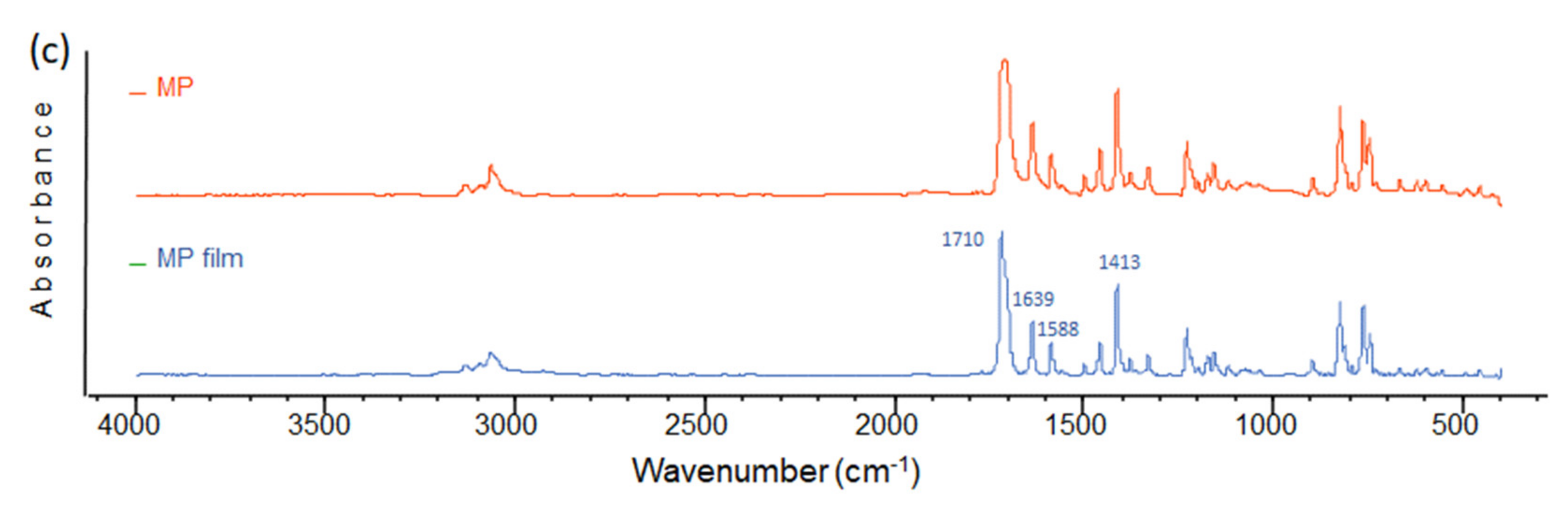
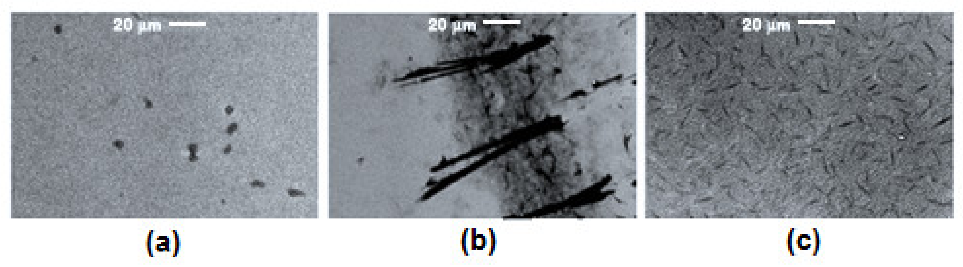
4.1. Deposit and Characterization of Pristine Maleiperinone Film

In order to study the optical and electrical behavior of thin films of MP as well as its possible application in optoelectronic devices, MP was initially deposited by vacuum evaporation. The topography and morphology are known to have a great influence on the optical and electrical properties exhibited by the MP thin films and depend on the preparation parameters of the film deposition. To study the surface roughness and topographical features of the prepared film an AFM was carried out. The 3D AFM image of the thin film is depicted in Figure 2a, and some voids are observed on the surface, although the film completely covers the substrate. In pristine MP film, the root mean square (RMS) roughness and the thickness values are recorded in Table 1. The RMS is in the order of 16.95 nm, indicating a relatively smoot surface. The SEM micrograph at 250× of MP film in Figure 2b shows a smooth and homogeneous surface with the formation of elongated structures randomly dispersed in the film. These structures are caused by the preferential directions in the growth process of some nuclei formed on the film initially deposited [10,12,13,35]. On the other hand, Figure 2c, shows the FTIR spectra of MP film, the bands appearing at 1710, 1639, 1588 and 1413 cm−1 are attributed to νC=O, νC=N, γ-heterocyclic system and νC-N bonds, respectively. The MP film spectrum was compared to the KBr pellet spectrum of the MP (see Figure 2c). The similarity between the two spectra is an indication of the ability of MP to form thin films, without undergoing chemical degradation. One of the main drawbacks of the use of organic semiconductors, with respect to inorganic ones such as silicon, is the low thermal stability [1,2,3,4,5,6]. Apparently, MP is a small molecule with high potential to compose uniform films by evaporation under vacuum.
Figure 3a shows the absorption spectra of MP film in the spectral range 280–1000 nm. The absorption spectrum shows strong transition in the visible region (450–550 nm) and in the UV region (280–315 nm). A maximum around 297 nm is observed in the spectrum, correspondent to the electronic transition n→π* towards the aromatic ring of naphthalene and an absorption band at 483 nm because of the charge transfer complex of the π electrons of the endocyclic double bond of the MP towards the heterocyclic ring [36]. Advanced UV-vis spectrum study of the prepared film was undertaken to determine the optical band gap (Eg). UV-vis spectrum data was used for point-by-point refinement of the absorption coefficient, α and the photon energy, hν [37,38]. The absorption coefficient is obtained by means of: α = l n T | d , where: T is the transmittance of the film (see Figure 3b), and d, is the thickness. The photon energy is obtained through: h ν = h c / λ , where h is the Planck constant, c represents the speed of light and λ is the wavelength. From α and values, Eg was obtained for direct and indirect transitions and based on the results it was determined whether the MP can be considered either as an indirect or direct band semiconductor. To obtain information about direct or indirect interband transitions, the fundamental absorption edge data can be analyzed within the framework of the one-electron theory of Bardeen et al. [38]. Indirect and direct transitions versus hν (see Equation (1)), are plotted in the Bardeen equation, which is depicted in Figure 3c [39,40],
α = α 0 h ν E g n
where the factor α0 depends on the transitions probability and can be assumed to be constant within the optical frequency range [37] and n is a number which describes the type of transition process, for direct transitions, n = ½, and for indirect transitions n = 2 [38,41,42]. Thus, the optical band gap for both transitions could be determined by the extrapolation to zero of the linear regions of the (αhυ)2 = f(hν) and (αhυ)½= f(hν) curves, Egd and Egi, respectively (Figure 3c) [38]. The extrapolation of this dependence to zero absorption yields a value of the Eg at the photon energy axis [37]. The obtained values of the fundamental band gap and onset band gap were determined and summarized in Table 1. The fundamental gap is the energy gap between valence band, π and conduction band π* whereas the onset gap corresponds to the onset of optical absorption and formation of Frenkel excitation [41,43]. The band gap of 2.71 and 2.06 eV for direct and indirect transitions, respectively, places the MP in the range of small semiconductor molecules. The dominant transitions are the indirect type, which is related to a predominantly amorphous character in the film. The thermal gradients during the deposition of the film, between the temperature of the MP and the temperature of the substrates, are responsible for the amorphous structure in the semiconductor film.

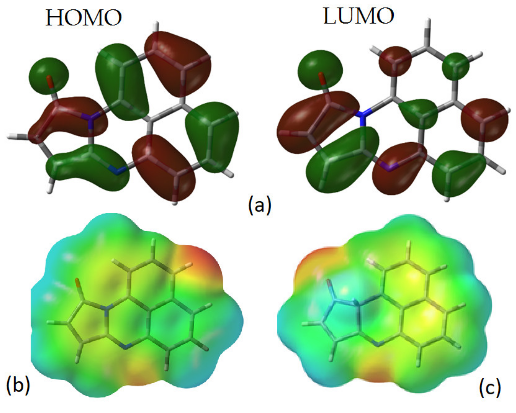
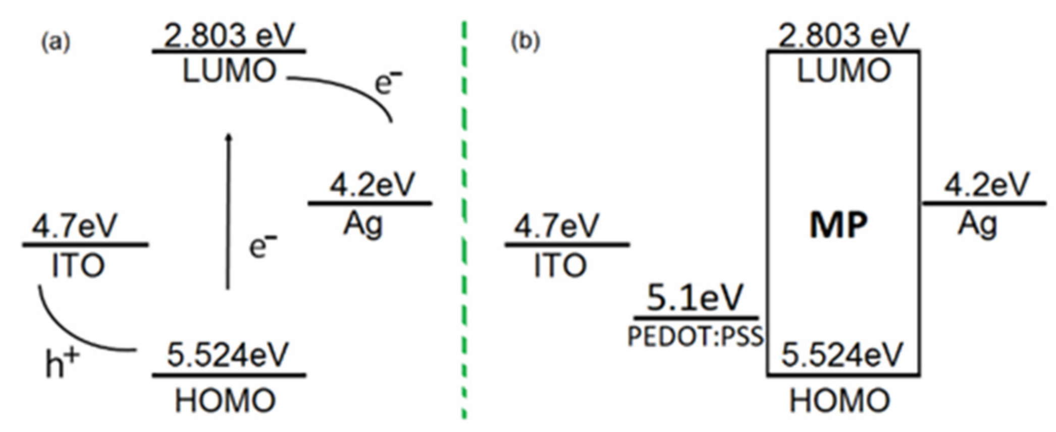
4.2. Theoretical Study

The electronic behavior of this compound is illustrated by the nature of its frontier molecular orbitals. Figure 4a shows HOMO and LUMO. The energy gap calculated between HOMO and LUMO is 2.721 eV, a result that suggests a semiconductor behavior. In addition, the value of this theoretical band gap is in the interval obtained for the experimental band gap (see Table 1). In other hand, there are important factors that influence the transport properties of the MP such as the dipole moment of the small molecule that according to the DFT calculations is 3.33 Db. This high polarity gives a signal of the heterogeneous charge distribution along the structure of MP. In Figure 4b the electrostatic potential mapped onto electron density is observed, the red zone represents the strong electronegative pole, one localized on the homocyclic region of the MP. The value of dipole moment arises from the interaction of this region with those electropositive shown in green-blue or blue colors. The presence of this negative charge density deserves an explanation because it seems to be stronger than those arising from the carbonyl group, the inductive effect caused by the nitrogen atoms found as heteroatoms in the aromatic framework gives place to this particularly negative region. The ring directly receiving the excess of electronic charge shows the nitrogenated substituent in para position with respect to the final negative charged region, therefore it is possible to consider that the sum of the inductive effect of this electron release group and the positive mesomeric effect of the oxygen group induces a strong electronic current that ends in the red zone of Figure 4b. A comparison is made with a model molecule where such a nitrogen atom was substituted by a methyl group, Figure 4c shows this case and the electrostatic potential mapped onto the electronic density shows the negative electronic densities on the oxygen and lateral nitrogen regions.

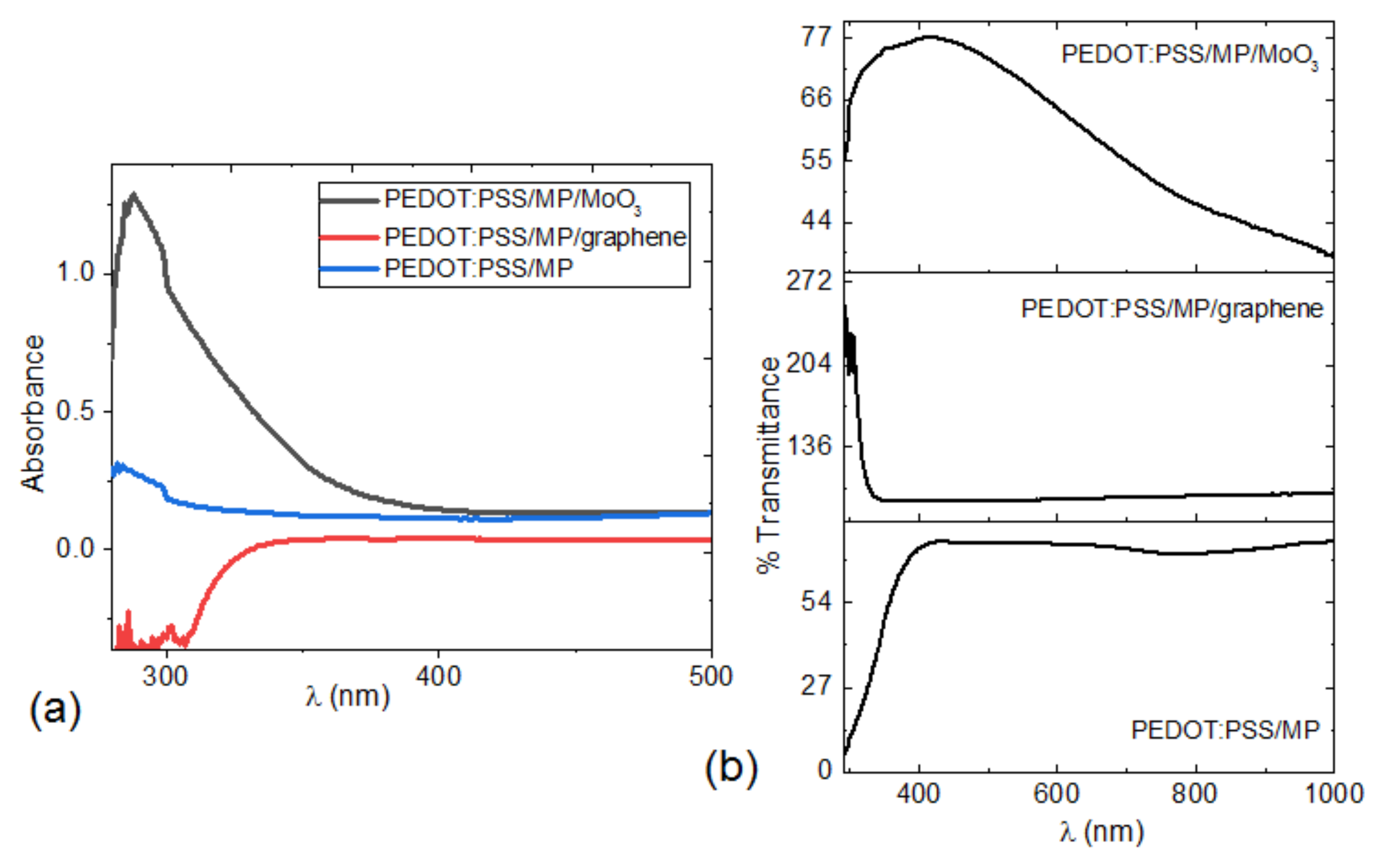
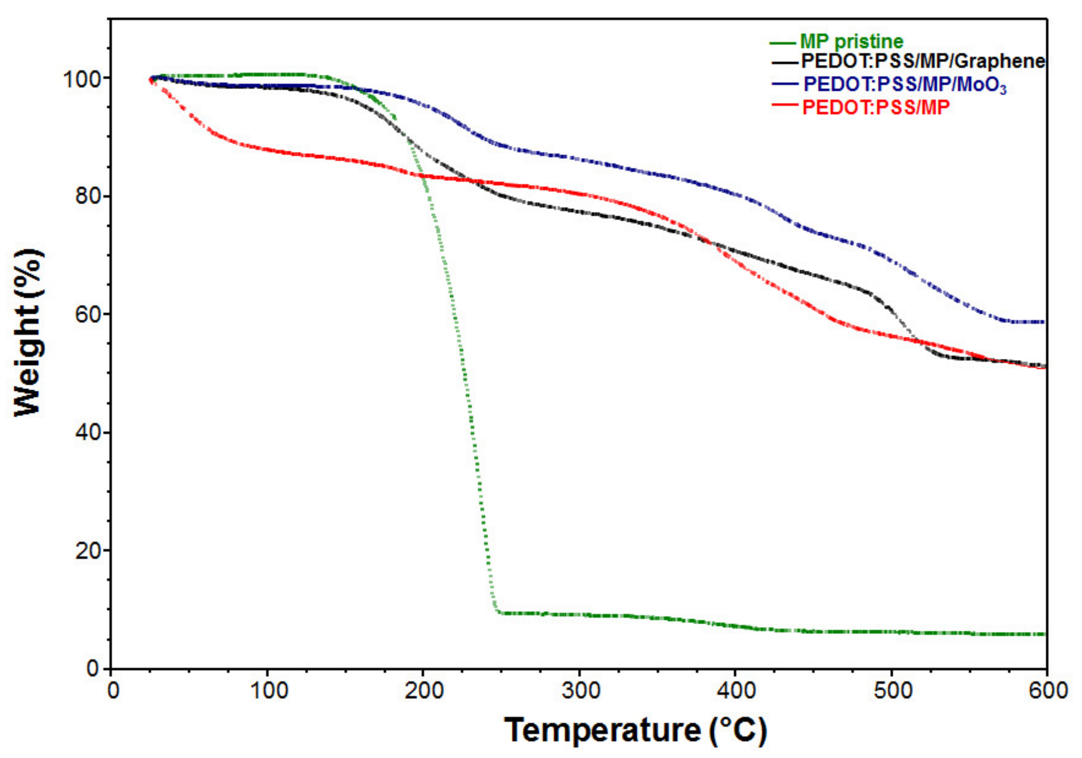
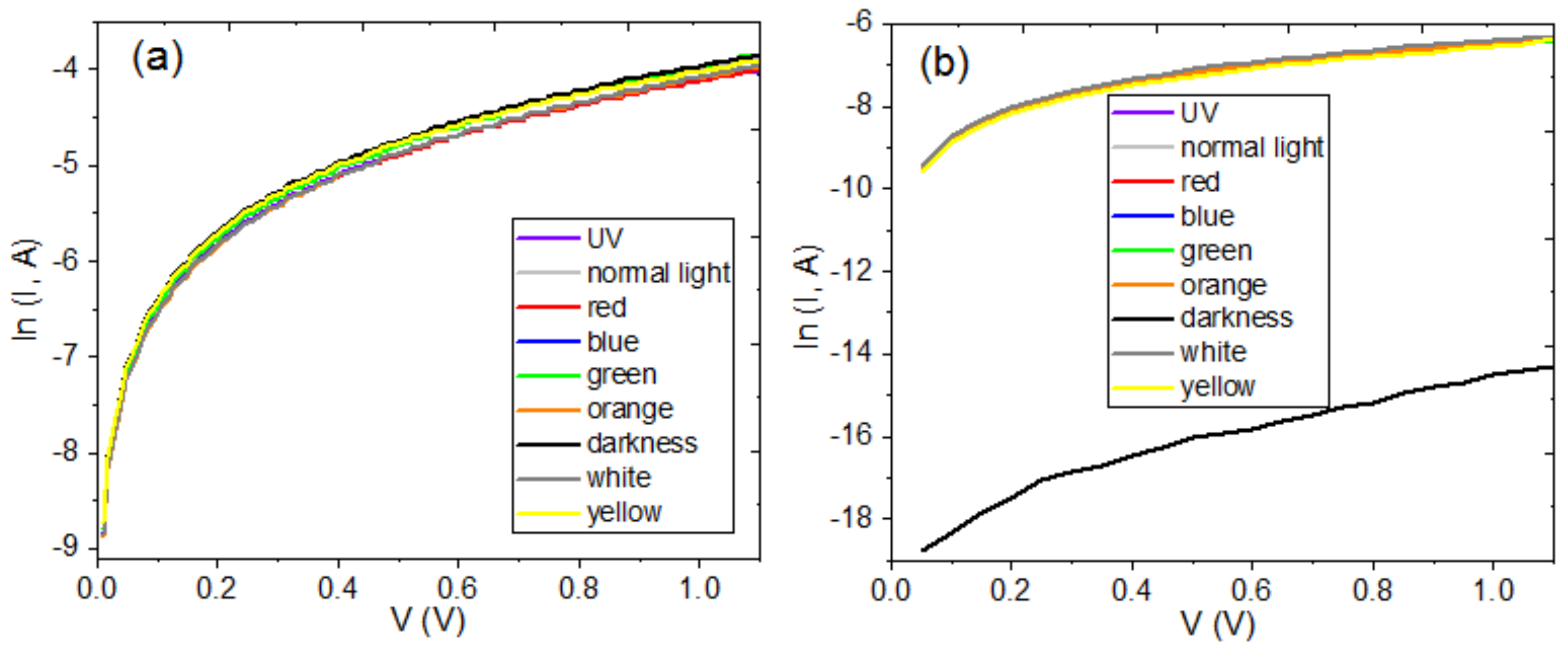
4.3. Deposit and Characterization of Hybrid Semiconductor Films

The evaluation of the electrical behavior took place in a simple device made from MP film. The ITO was used as anode, while the Ag was deposited as cathode. The current (I) vs. voltage (V) of the pristine MP was estimated in the presence of radiation of different wavelengths between the IR and the UV of the electromagnetic spectrum. According to Figure 5a, it is expected to generate a device with ohmic contact, where different phenomena can take place. After the electrons are displaced from the HOMO to the LUMO of the MP, they will be injected-extracted towards the Ag. On the other hand, the hollow created in HOMO will be transferred to the ITO without the generation of energy barriers that hinder the charge injection-extraction process. The MP behaves as a p-type semiconductor or hole transporter, and its HOMO level with respect to the ITO work function allows for easy injection and high mobility of holes. According to the graph of Figure 6a, the behavior of the device ITO/MP/Ag is basically ohmic and there is no dependence between the current transported, and the wavelength irradiated to the device. In order to enhance the electrical behavior of the MP, hybrid films were deposited using the PEDOT:PSS as a matrix. Figure 5b shows how the polymer, with a work function of 5.1 eV [44], behaves as a kind of hole injector layer [21], and it is expected to favor the transport of charges between the MP that acts as a p-type semiconductor and the ITO. Additionally, the MP/PEDOT:PSS film was treated with the dopant’s graphene and MoO3. The presence of dopants is intended to facilitate the transport of charges in the device [21,25,26,27,28]. Figure 6b shows the ln I-V graph for the film of pristine PEDOT:PSS, it is observed that in a similar way to the device made with the MP (Figure 6a), the polymer shows ohmic behavior under different lighting conditions; furthermore, it shows insulating behavior in dark conditions or lack of radiation. These results will allow to compare the effect of both MP and polymer in the hybrid films.
After the manufacturing of the films PEDOT:PSS/MP, PEDOT:PSS/MP/graphene and PEDOT:PSS/MP/MoO3, their topography and morphology were studied using AFM and SEM. Figure 7a shows the AFM image, while the Table 1 shows the RMS and the thickness values for the film PEDOT:PSS/MP, and additionally for the films doped with graphene (Figure 7b) and MoO3 (Figure 7c). The difference in topography between the three films is evident, and RMS values in Table 1 are ranged in-between 15.92 nm and 58.75 nm. An important fact is that the RMS of the pristine MP film (16.95 nm) is very similar to the one obtained in the film PEDOT:PSS/MP (15.92 nm). The lowest roughness value obtained for the PEDOT:PSS/MP structure can be explained by a proper arrangement of the MP molecules on the PEDOT:PSS matrix. The PEDOT:PSS/MP is more homogenous than the PEDOT:PSS/MP/graphene and PEDOT:PSS/MP/MoO3 structures, the presence of the dopant particles increases the rugosity (58.75 and 34.97 respectively). According to Pasha et al., the increase in RMS in doped PEDOT:PSS/MP films may be due to the thinning effect after the interaction of dopants in PEDOT:PSS [45]. As dopants readily interact in the dispersion with PEDOT and PSS chains, a denser morphology is formed in doped PEDOT-PSS films. This is confirmed by the SEM micrographs at 750× shown in Figure 8, different molecular organizations in the films are observed. The micrograph of PEDOT:PSS/MP film (see Figure 8a), shows a smooth and homogeneous surface with the formation of some micro-granules in the surface. In contrast, the inclusion of dopants in PEDOT:PSS show macrostructures dispersed in the matrix, these particles are clearly observed. PEDOT:PSS/MP/graphene film (Figure 8b) exhibits rougher surface with larger and columnar structures and PEDOT:PSS/MP/MoO3 film (Figure 8c) shows a relatively homogeneous dispersion of elongated structures on a granular matrix. Columnar and elongated structures in dopant films are the result of nucleation and growth in preferential directions of the MP. Deposition conditions and interactions with the substrate surface play a critical role in determining the film continuity as well as the structure and crystalline grain size within the film [46]. Since the substrates and deposit conditions of the films were the same for the three different types of film, it is evident that the presence of the doping particles influences the structure of these films.
Figure 9a shows the absorbance spectrum for each hybrid film. Comparing this figure with the spectrum in Figure 3a, the presence of PEDOT:PSS decreases the absorption of the MP, over all in the region around 483 nm, correspondent to the band generated by the transfer of the π electrons of the double endocyclic bond, towards the heterocyclic ring [36]. This effect is more significant when graphene is used (see Figure 9a), since this film does not present absorption in its spectrum. The decrease in absorption in these two films may be due to the type and morphology of dispersed heterojunction formed. By supplementing this information with the transmittance spectra in Figure 9b, it is observed that the film PEDOT:PSS/MP transmitted more than 73% of light in the wavelength region of 400–1000 nm. Nevertheless, PEDOT:PSS/MP/graphene film does not show optical behavior. The film containing graphene shows a suppressed transmittance [26]. On the other hand, when MoO3 is the chosen dopant (see Figure 9a), the band is kept at 297 nm corresponding to the transitions n→π* towards the aromatic ring of the naphthalene. Transmission spectra of PEDOT:PSS/MP/MoO3 is shown in Figure 9b. The transmittance at 400 nm is 77% and decrease throughout the visible range [25]. Due to the good optical transparency of the PEDOT:PSS/MP and PEDOT:PSS/MP/MoO3 films, they would be an effective option to use in the field of organic electronics [25,26,27]. The band gap values for indirect and direct transitions, are reported in Table 1, in the films PEDOT:PSS/MP and PEDOT:PSS/MP/MoO3, the band gap increases considerably, with respect to the one obtained in the film of pristine MP. Whereas in the film PEDOT:PSS/MP/graphene, no semiconductor behavior was found, then, the obtention of the band gap value was not possible.
Regarding the electrical features, Figure 10a–c show that in a similar way to the optical behavior, the electrical properties are completely modified in the films. Figure 10a illustrates the ln I-V characteristics of ITO/PEDOT:PSS/MP/Ag at different electromagnetic radiation. The results show that the curves have the same ln I-V behavior and the current increases under natural or normal illumination condition. Two distinct regions characterize these curves indicating two different conduction mechanisms. At V < 0.65 V the current increases exponentially with the applied voltage, while at V ≥ 0.65 V, the current is deviated due to a voltage drop across the resistance associated with the neutral region of a semiconductor and interface states [47]. In the Figure 10b, corresponding to the device ITO/PEDOT:PSS/MP/graphene/Ag, the same behavior is present in all the curves. At applied V < 0.1 V, the logarithm of the current increases linearly with increasing applied voltage; this indicates that thermionic emission conduction is the predominant conduction mechanism [48]. For the device ITO/PEDOT:PSS/MP/MoO3/Ag the behavior can be studied only, in the curve obtained under normal lighting conditions and it is an exponential behavior. The rest of the curves show a linear behavior at V ≥ 0.6 V. The incorporation of the PEDOT: PSS in the films of the devices, reduces the energy barrier between the ITO and the maleiperinone and modifies the electrical behavior in the devices. Additionally, the presence of the dopants graphene and MoO3, generated particular behaviors in the devices. On the one hand, graphene decreased the absorption in the film and added to its ohmic behavior, giving it the potential to be used as a transparent electrode in optoelectronic devices. In the case of the hybrid film doped with MoO3, the effect is less significant, because it decreases the transport of charges in the device by several orders of magnitude. This film could function as a dielectric material in organic transistors. The surface resistance results are shown in Table 2 for normal lighting conditions at 0.5 and 1 V. Films with graphene and MoO3 dopants are the ones with the least resistance and are more likely to be used in optoelectronic devices.
Finally, Figure 11 shows the thermogram of MP pristine, PEDOT:PSS/MP/graphene, PEDOT: PSS/MP/MoO3, and PEDOT:PSS/MP films. Thermogravimetric analysis of the MP pristine film shows that MP decomposes into a single phase and begins to lose weight after its melting point at 130 °C. PEDOT: PSS/MP/graphene, PEDOT:PSS/MP/MoO3, and PEDOT:PSS/MP films compared to pristine MP film show weight losses greater than 250 °C, which indicates proper operating ranges, this is important for many optoelectronics applications. In these films, the weight losses less than 150 °C are attributed to the water absorbed by PEDOT:PSS, while weight losses greater than 250 °C are attributed to the breakdown of the sulfonate group of PSS. The steepest weight loss was observed at 400 °C, which is attributed to the degradation of the polymer backbone and the oxidation of graphene, in addition the film containing MoO3 is the one with the best thermal stability.

5. Conclusions

Initially, pristine maleiperinone was deposited using the high-vacuum thermal evaporation technique. The band gap obtained for direct electronic transitions (2.82 eV), and for indirect ones (2.09 eV), places maleiperinone within the family of organic semiconductors. Additionally, the DFT analysis found a high polarity and a heterogeneous charge distribution in maleiperinone. The band gap calculated is in the range obtained experimentally. With the semiconductor maleiperinone, composite films were deposited using PEDOT:PSS as a matrix and additionally, films were made with the dopants graphene and MoO3. The presence of the polymer decreased the energy barrier between the semiconductor film and the anode, favoring the transport of charges in the device. Graphene decreased the absorption of the film and its ohmic behavior make it a candidate to be used as a transparent electrode in optoelectronic devices. The MoO3 in the hybrid film provides a behavior similar to a dielectric. Thermogravimetric analysis of the films shows that the film containing MoO3 is the one with the best thermal stability.

Author Contributions

Conceptualization, M.E.S.V., S.B.R. and R.S.; methodology, M.E.S.V., S.B.R., R.L.A., M.D.B.A., C.R. and R.S.; software M.E.S.V., R.L.A., C.R. and R.S.; validation, M.E.S.V., S.B.R., L.F., M.D.B.A. and R.S.; formal analysis, M.E.S.V., S.B.R., L.F., M.D.B.A. and R.S.; investigation, M.E.S.V., S.B.R., G.M.d.O.R., C.R. and R.S.; resources, M.E.S.V. and M.D.B.A.; data curation, M.E.S.V., S.B.R. and R.S.; writing—original draft preparation, M.E.S.V., S.B.R., C.R. and R.S.; writing—review and editing, M.E.S.V., S.B.R., L.F., C.R., G.M.d.O.R. and R.S.; visualization, M.E.S.V., R.L.A., G.M.d.O.R. and R.S.; supervision, M.E.S.V.; project administration, M.E.S.V.; funding acquisition, M.E.S.V. All authors have read and agreed to the published version of the manuscript.

Funding

María Elena Sánchez-Vergara acknowledges the financial support from Anahuac Mexico University, Project number NNAIASEVM16070616. Sergio Barrientos Ramírez acknowledges financial support from DESC Group by DESC Research Chair.

Institutional Review Board Statement

Not applicable.

Informed Consent Statement

Not applicable.

Data Availability Statement

Not applicable.

Acknowledgments

Thanks to Oralia Jiménez and Teresa Vázquez for technical help.

Conflicts of Interest

The authors declare no conflict of interest.

References

  1. Hains, A.W.; Liang, Z.; Woodhouse, M.A.; Gregg, B.A. Molecular Semiconductors in Organic Photovoltaic Cells. Chem. Rev. 2010, 110, 6689–6735. [Google Scholar] [CrossRef] [PubMed]
  2. Shaheen, S.E.; Ginley, D.S.; Jabbour, G.E. Organic-Based Photovoltaics: Toward low-cost power generation. MRS Bull. 2005, 30, 10–19. [Google Scholar] [CrossRef] [Green Version]
  3. Günes, S.; Neugebauer, H.; Sariciftci, N.S. Conjugated polymer-based organic solar cells. Chem. Rev. 2007, 107, 1324–1338. [Google Scholar] [CrossRef]
  4. Yoo, S.; Domercq, B.; Kippelen, B. Efficient thin-film organic solar cells based on pentacene/C60 heterojunctions. Appl. Phys. Lett. 2004, 85, 5427–5429. [Google Scholar] [CrossRef] [Green Version]
  5. Dong, H.; Zhu, H.; Meng, Q.; Gong, X.; Hu, W. Organic photoresponse materials and devices. Chem. Soc. Rev. 2012, 41, 1754–1808. [Google Scholar] [CrossRef]
  6. Dong, H.; Wang, C.; Hu, W. High performance organic semiconductors for field-effect transistors. Chem. Commun. 2010, 46, 5211–5222. [Google Scholar] [CrossRef] [PubMed]
  7. Scharber, M.C.; Sariciftci, N.S. Low band gap conjugated semiconducting polymers. Adv. Mater. Technol. 2021, 6, 2000857. [Google Scholar] [CrossRef]
  8. Barbot, A.; Di Bin, C.; Lucas, B.; Ratier, B.; Aldissi, M. N-type doping and thermoelectric properties of co-sublimed cesium-carbonate-doped fullerene. J. Mater. Sci. 2013, 48, 2785–2789. [Google Scholar] [CrossRef]
  9. Husain, A.A.F.; Hasan, W.Z.W.; Shafie, S.; Hamidon, M.N.; Pandey, S.S. A review of transparent solar photovoltaic technologies. Renew. Sustain. Energy Rev. 2018, 94, 779–791. [Google Scholar] [CrossRef]
  10. Cranston, R.R.; Lessard, B.H. Metal phthalocyanines: Thin-film formation, microstructure, and physical properties. RSC Adv. 2021, 11, 21716–21737. [Google Scholar] [CrossRef]
  11. Hoppe, H.; Sariciftci, N.S. Organic solar cells: An overview. J. Mater. Res. 2004, 19, 1924–1945. [Google Scholar] [CrossRef] [Green Version]
  12. Schubert, D.W.; Dunkel, T. Spin coating from a molecular point of view: Its concentration regimes, influence of molar mass and distribution. Mat. Res. Innovat. 2003, 7, 314–321. [Google Scholar] [CrossRef]
  13. Alfredo, N.V.; Likhatchev, D.; Ramirez, S.B.; Vazquez, J.R.; Valverde, G.C.; Alexandrova, L. Highly effective low temperature route to pyrroloperimidines synthesis and their copolymerization with styrene and methyl methacrylate. Polymer 2008, 49, 3654–3662. [Google Scholar] [CrossRef]
  14. Koca, R.; Ngren, E.H.; Kbrz, B.E.; Ylmaz, F. The synthesis of new pyrrolo[1,2-a]perimidin-10-one dyes via two convenient routes and its characterizations. Dyes Pigm. 2012, 95, 421–426. [Google Scholar] [CrossRef]
  15. Fernández-Gijón, C.A.; del Río-Portilla, F.; Ríos-Jara, D.; Fomine, S.; Santana, G.; Alexandrova, L. Itaco-perinone as a molecule with potential use in white light emitting materials. The effect of methyl- and methylene groups on the formation of perimidine and perinone structures. Tetrahedron 2015, 71, 7063–7069. [Google Scholar] [CrossRef]
  16. Nuñez Bahena, E.; Fernández Gijón, C.A.; Fomine, S.; Alexandrova, L.; Le Lagadec, R. Synthesis, characterization, and spectroscopic properties of allylic ruthenium(II) complexes of a highly conjugated perinone. Eur. J. Inorg. Chem. 2019, 2019, 3494–3502. [Google Scholar] [CrossRef]
  17. Erten, S.; Icli, S. Bilayer heterojunction solar cell based on naphthalene bis-benzimidazole. Inorg. Chim. Acta 2008, 361, 595–600. [Google Scholar] [CrossRef]
  18. Faraonov, M.A.; Romanenko, N.R.; Mikhailenko, M.V.; Kuzmin, A.V.; Khasanov, S.S.; Konarev, D.V. Structure and properties of radical anion and dianion salts of organic dye trans-perinone and its mixed salt with gallium(iii) phthalocyanine. New J. Chem. 2021, 45, 13599–13607. [Google Scholar] [CrossRef]
  19. Wang, H.-Y.; Gao, J.; Gu, L.-J.; Wan, J.-H.; Wei, W.; Liu, F. Structural modification of thieno[3,4-c]pyrrole-4,6-dione: Structure–property relationships and application in solution-processed small-molecule organic solar cells. J. Mater. Chem. A Mater. Energy Sustain. 2013, 1, 5875. [Google Scholar] [CrossRef]
  20. Yeo, J.-S.; Yun, J.-M.; Kim, D.-Y.; Park, S.; Kim, S.-S.; Yoon, M.-H.; Kim, T.-W.; Na, S.-I. Significant vertical phase separation in solvent-vapor-annealed poly(3,4-ethylenedioxythiophene):poly(styrene sulfonate) composite films leading to better conductivity and work function for high-performance indium tin oxide-free optoelectronics. ACS Appl. Mater. Interfaces 2012, 4, 2551–2560. [Google Scholar] [CrossRef] [PubMed]
  21. Yoo, D.; Kim, J.; Kim, J.H. Direct synthesis of highly conductive poly(3,4-ethylenedioxythiophene):poly(4-styrenesulfonate) (PEDOT:PSS)/graphene composites and their applications in energy harvesting systems. Nano Res. 2014, 7, 717–730. [Google Scholar] [CrossRef]
  22. Neophytou, M.; Griffiths, J.; Fraser, J.; Kirkus, M.; Chen, H.; Nielsen, C.B.; McCulloch, I. High mobility, hole transport materials for highly efficient PEDOT:PSS replacement in inverted perovskite solar cells. J. Mater. Chem. C Mater. Opt. Electron. Devices 2017, 5, 4940–4945. [Google Scholar] [CrossRef] [Green Version]
  23. Zhang, W.; Bi, X.; Zhao, X.; Zhao, Z.; Zhu, J.; Dai, S.; Lu, Y.; Yang, S. Isopropanol-treated PEDOT:PSS as electron transport layer in polymer solar cells. Org. Electron. 2014, 15, 3445–3451. [Google Scholar] [CrossRef]
  24. Yeon, C.; Kim, G.; Lim, J.W.; Yun, S.J. Highly conductive PEDOT:PSS treated by sodium dodecyl sulfate for stretchable fabric heaters. RSC Adv. 2017, 7, 5888–5897. [Google Scholar] [CrossRef] [Green Version]
  25. Kepić, D.; Markovic, Z.; Jovanović, S.P.; Perusko, D.; Budimir, M.; Holclajtner-Antunović, I.D.; Pavlović, V.; Marković, B.T. Preparation of PEDOT:PSS thin films doped with graphene and graphene quantum dots. Synth. Met. 2014, 198, 150–154. [Google Scholar] [CrossRef]
  26. Chen, Q.; Zabihi, F.; Eslamian, M. Improved functionality of PEDOT:PSS thin films via graphene doping, fabricated by ultrasonic substrate vibration-assisted spray coating. Synth. Met. 2016, 222, 309–317. [Google Scholar] [CrossRef]
  27. Hilal, M.; Han, J.I. Improving the conductivity of PEDOT:PSS to nearly 1 million S/m with graphene on an ITO-glass substrate. Synth. Met. 2018, 245, 276–285. [Google Scholar] [CrossRef]
  28. Lattante, S. Electron and Hole Transport Layers: Their Use in Inverted Bulk Heterojunction Polymer Solar Cells. Electronics 2014, 3, 132–164. [Google Scholar] [CrossRef]
  29. Gao, H.; Zhao, X.; Zhang, H.; Chen, J.; Wang, S.; Yang, H. Construction of 2D/0D/2D face-to-face contact g-C3N4@Au@Bi4Ti3O12 heterojunction photocatalysts for degradation of rhodamine B. J. Electron. Mater. 2020, 49, 5248–5259. [Google Scholar] [CrossRef]
  30. Leung, S.-F.; Zhang, Q.; Xiu, F.; Yu, D.; Ho, J.C.; Li, D.; Fan, Z. Light management with nanostructures for optoelectronic devices. J. Phys. Chem. Lett. 2014, 5, 1479–1495. [Google Scholar] [CrossRef]
  31. Becke, A.D. Density-functional exchange-energy approximation with correct asymptotic behavior. Phys. Rev. A Gen. Phys. 1988, 38, 3098–3100. [Google Scholar] [CrossRef]
  32. Perdew, J.P.; Wang, Y. Accurate and simple analytic representation of the electron-gas correlation energy. Phys. Rev. B Condens. Matter 1992, 45, 13244–13249. [Google Scholar] [CrossRef] [PubMed]
  33. Frisch, M.J.; Trucks, G.W.; Schlegel, H.B.; Scuseria, G.E.; Robb, M.A.; Cheeseman, J.R.; Scalmani, G.; Barone, V.; Mennucci, B.; Petersson, G.A.; et al. Gaussian 09, Revision A.1; Fox, Gaussian, Inc.: Wallingford, UK, 2009. [Google Scholar]
  34. Grimme, S.; Antony, J.; Ehrlich, S.; Krieg, H. A consistent and accurate ab initio parametrization of density functional dispersion correction (DFT-D) for the 94 elements H-Pu. J. Chem. Phys. 2010, 132, 154104. [Google Scholar] [CrossRef] [PubMed] [Green Version]
  35. Venables, J.A. Atomic processes in crystal growth. Surf. Sci. 1994, 299–300, 798–817. [Google Scholar] [CrossRef]
  36. Silverstein, R.M.; Webster, F.X.; Kiemle, D.J. The Spectrometric Identification of Organic Compounds, 7th ed.; John Wiley & Sons: Nashville, TN, USA, 2005. [Google Scholar]
  37. Novotny, M.; Bulir, J.; Bensalah-Ledoux, A.; Guy, S.; Fitl, P.; Vrnata, M.; Lancok, J.; Moine, B. Optical properties of zinc phthalocyanine thin films prepared by pulsed laser deposition. Appl. Phys. A Mater. Sci. Process. 2014, 117, 377–381. [Google Scholar] [CrossRef]
  38. Sánchez-Vergara, M.E.; Rivera, M.; Alonso-Huitrón, J.C.; Rodriguez, A.; Álvarez-Bada, J.R. Electrical and optical properties of copper-complexes thin films grown by the vacuum thermal evaporation technique. Mater. Chem. Phys. 2013, 138, 392–398. [Google Scholar] [CrossRef]
  39. Breckenridge, R.G.; Russell, B.R.; Hahn, E.E. Proceedings of the Photoconductivity Conference; Wiley: New York, NY, USA, 1956. [Google Scholar]
  40. Urbach, F. The long-wavelength edge of photographic sensitivity and of the electronic absorption of solids. Phys. Rev. 1953, 92, 1324. [Google Scholar] [CrossRef]
  41. El-Nahass, M.M.; Hassanien, A.M.; Abu-Samaha, F.S.H.; Elesh, E. Effect of illumination on the structural and optical properties of Cu (II) tetraphenyl porphyrin (CuTPP) thin films. Opt. Commun. 2014, 325, 116–121. [Google Scholar] [CrossRef]
  42. El-Nahass, M.M.; Abd-El-Rahman, K.F.; Al-Ghamdi, A.A.; Asiri, A.M. Optical properties of thermally evaporated tin-phthalocyanine dichloride thin films, SnPcCl2. Phys. B Condens. Matter. 2004, 344, 398–406. [Google Scholar] [CrossRef]
  43. Tsiper, E.V.; Soos, Z.G.; Gao, W.; Kahn, A. Electronic polarization at surfaces and thin films of organic molecular crystals: PTCDA. Chem. Phys. Lett. 2002, 360, 47–52. [Google Scholar] [CrossRef] [Green Version]
  44. Zubair, M.; Mustafa, M.; Ali, A.; Doh, Y.H.; Choi, K.H. Improvement of solution based conjugate polymer organic light emitting diode by ZnO–graphene quantum dots. J. Mater. Sci. Mater. Electron. 2015, 26, 3344–3351. [Google Scholar] [CrossRef]
  45. Pasha, A.; Khasim, S.; Khan, F.A.; Dhananjaya, N. Fabrication of gas sensor device using poly (3,4-ethylenedioxythiophene)-poly (styrenesulfonate)-doped reduced graphene oxide organic thin films for detection of ammonia gas at room temperature. Iran. Polym. J. 2019, 28, 183–192. [Google Scholar] [CrossRef]
  46. Murphy, A.R.; Fréchet, J.M.J. Organic semiconducting oligomers for use in thin film transistors. Chem. Rev. 2007, 107, 1066–1096. [Google Scholar] [CrossRef]
  47. Soliman, I.M.; El-Nahass, M.M.; Khalifa, B.A. Characterization and photovoltaic performance of organic device based on AlPcCl/p-Si heterojunction. Synth. Met. 2015, 209, 55–59. [Google Scholar] [CrossRef]
  48. Zeyada, H.M.; El-Nahass, M.M.; El-Menyawy, E.M.; El-Sawah, A.S. Electrical and photovoltaic characteristics of indium phthalocyanine chloride/p-Si solar cell. Synth. Met. 2015, 207, 46–53. [Google Scholar] [CrossRef]
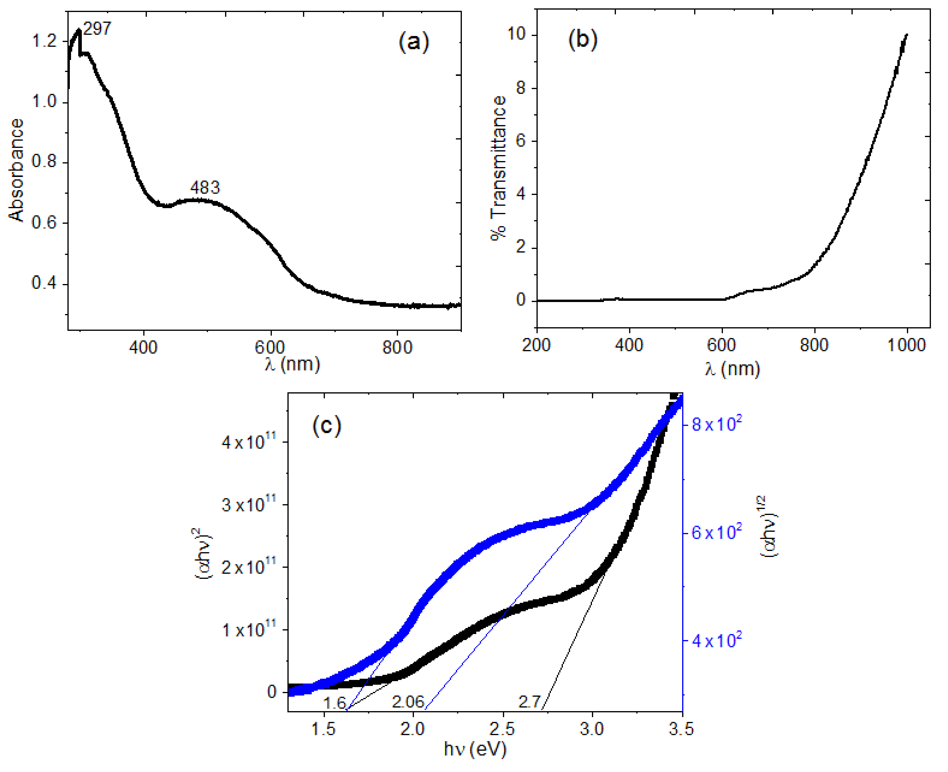
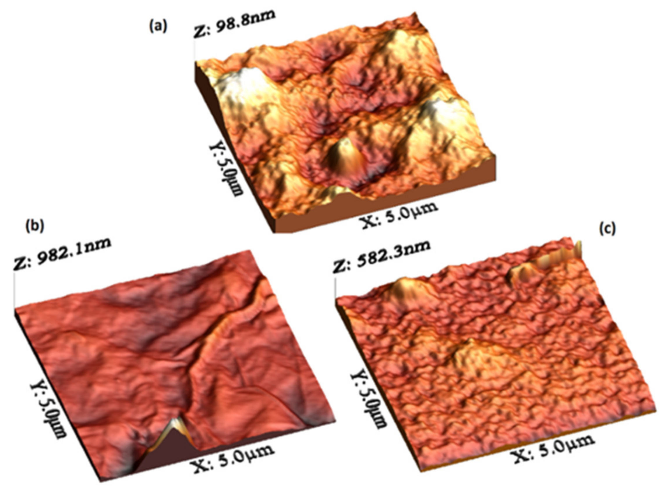
Figure 1. Structure of the (a) MP and (b) PEDOT:PSS.
Processes 09 01776 g001
Figure 2. (a) AFM image, (b) SEM image and (c) IR spectrum for the pristine film of MP.
Processes 09 01776 g002aProcesses 09 01776 g002b
Figure 3. (a) Absorbance and (b) Transmittance spectrum. (c) Direct and indirect transitions for the pristine film of MP.
Processes 09 01776 g003
Figure 4. (a) Structure and frontier molecular orbitals HOMO and LUMO and (b) Electrostatic potential mapped on the electron density for MP and (c) analogue of MP with a methyl instead of nitrogen atom.
Processes 09 01776 g004
Figure 5. Schematic energy level diagram of the device (a) ITO/MP/Ag and (b) ITO/PEDOT:PSS/MP/Ag.
Processes 09 01776 g005
Figure 6. ln I vs. V characteristics for (a) ITO/MP/Ag and (b) ITO/PEDOT:PSS/Ag devices at different radiation conditions.
Processes 09 01776 g006
Figure 7. AFM images of (a) PEDOT:PSS/MP, (b) PEDOT:PSS/MP/graphene and (c) PEDOT:PSS/MP/MoO3 films.
Processes 09 01776 g007
Figure 8. SEM micrographs of (a) PEDOT:PSS/MP, (b) PEDOT:PSS/MP/graphene and (c) PEDOT:PSS/MP/MoO3 films.
Processes 09 01776 g008
Figure 9. (a) Absorbance and (b) transmittance spectrum of hybrid films.
Processes 09 01776 g009
Figure 10. Ln I-V characteristics of (a) ITO/PEDOT:PSS/MP/Ag, (b) ITO/PEDOT:PSS/MP/graphene/Ag and (c) ITO/PEDOT:PSS/MP/MoO3/Ag devices.
Processes 09 01776 g010
Figure 11. TGA thermogram of MP pristine, PEDOT:PSS/MP/graphene, PEDOT:PSS/MP/MoO3, and PEDOT:PSS/MP films.
Processes 09 01776 g011
Table 1. Rugosity and optical parameters for the films based in MP.
FilmThickness (μm)RMS (nm)Onset Band Gap(eV)Energy
Band Gap. Direct Transitions (eV)
Energy
Band Gap.
Indirect Transitions (eV)
Pristine MP1.416.951.62.712.06
PEDOT:PSS/MP0.98815.92-3.923.60
PEDOT:PSS/MP/graphene1.0658.75---
PEDOT:PSS/MP/MoO31.034.97-3.722.83
Table 2. Surface resistance of devices.
Sample0.5 V1.0 V
ITO/MP/Ag3.6 × 104 Ω1.8 × 10⁴ Ω
ITO/PEDOT:PSS/MP/Ag2.2 × 108 Ω1.1 × 10⁸ Ω
ITO/PEDOT:PSS/MP/graphene/Ag50 Ω43 Ω
ITO/PEDOT:PSS/MP/MoO3/Ag59 Ω54 Ω
Publisher’s Note: MDPI stays neutral with regard to jurisdictional claims in published maps and institutional affiliations.

