Article

Time of Flight Size Control of Carbon Nanoparticles Using Ar+CH4 Multi-Hollow Discharge Plasma Chemical Vapor Deposition Method

1
Department of Electronics, Kyushu University, Fukuoka 819-0395, Japan
2
Center for Novel Science Initiatives, National Institutes of Natural Science, Tokyo 105-0001, Japan
3
Center of Plasma Nano-Interface Engineering, Kyushu University, Fukuoka 819-0395, Japan
4
Graduate School of Engineering, Osaka City University, Osaka 558-8585, Japan
5
National Institute of Technology, Ariake College, Fukuoka 836-8585, Japan
6
Institute of Frontier Science and Technology, Okayama University of Science, Okayama 700-0005, Japan
*
Author to whom correspondence should be addressed.
Processes 2021, 9(1), 2; https://doi.org/10.3390/pr9010002
Submission received: 13 November 2020 / Revised: 14 December 2020 / Accepted: 16 December 2020 / Published: 22 December 2020
(This article belongs to the Special Issue Advances in Plasma Diagnostics and Applications)

Abstract

:
As the application of nanotechnology increases continuously, the need for controlled size nanoparticles also increases. Therefore, in this work, we discussed the growth mechanism of carbon nanoparticles generated in Ar+CH4 multi-hollow discharge plasmas. Using the plasmas, we succeeded in continuous generation of hydrogenated amorphous carbon nanoparticles with controlled size (25–220 nm) by the gas flow. Among the nanoparticle growth processes in plasmas, we confirmed the deposition of carbon-related radicals was the dominant process for the method. The size of nanoparticles was proportional to the gas residence time in holes of the discharge electrode. The radical deposition developed the nucleated nanoparticles during their transport in discharges, and the time of flight in discharges controlled the size of nanoparticles.

1. Introduction

Carbon nanoparticles (CNPs) have attracted tremendous attention for their various applications, such as electrical conductivity improvement of polymer, lubrication applications, cancer cell treatments, bioimaging diagnostics [1,2,3]. Therefore, it is essential to develop a simple method to control the size and structure of CNPs [4,5,6,7]. The solution process is a conventional method of producing CNPs, but this method has limitations like impurity, unexpected agglomeration, and low throughput due to the multistage process [8,9,10,11].
The plasma process plays a promising role because it is a dry process using low pressure resulting from reducing impurity and avoid agglomeration or coagulation due to the charge of CNPs. However, the traditional plasma process has a problem regarding throughput due to pulsed discharges for size control [12,13,14]. Traditional plasma process has the discharge off period to wait for pumping out the particles from the gas phase, resulting in lower throughput.
To date, we have successfully synthesized Si NPs and CNPs by using multi-hollow discharge plasma chemical vapor deposition (MHDPCVD), which can be produced continuously by employing fast gas flow [15,16,17,18,19,20,21,22,23]. In this method, the gas flow direction is uniform in the plasma region, and NPs are nucleated and grown in plasma. The nucleated NPs were transported toward the outside of the plasmas by viscous gas force. That results in stopped growth outside of the plasma, which helped in the continuous production of size-controlled NPs.
NPs synthesis by the MHDPCVD method undergoes parametric tests such as dependence on gas pressure, gas flow rate, and gas composition, which are the external parameters [15,16,17,18,19,20,21,22,23,24]. Using the MHDPCVD, crystalline Si nanoparticles of 2 nm in size with 0.5 nm in size dispersion were produced for nanocrystalline amorphous silicon films for the third generation solar cells [15,16,17,18,19,20,21]. We employed two MHDPCVD sources to produce size-controlled Si nanoparticles and to cover nitrogen on the particles. The surface-modified nanoparticles showed multi-exciton generation, which is necessary to increase solar cells’ efficiency [18]. We recently used MHDPCVD to produce carbon nanoparticles [23,24,25] and confirmed that pressure played an important role in size control [23]. These studies revealed the essential parameters for the size control, while the growth mechanism was unclear. Hence, in this study, we measured the CNPs size dependence on the gas flow rate (FR) and discussed the growth mechanism of nanoparticles produced by the MHDPCVD method.

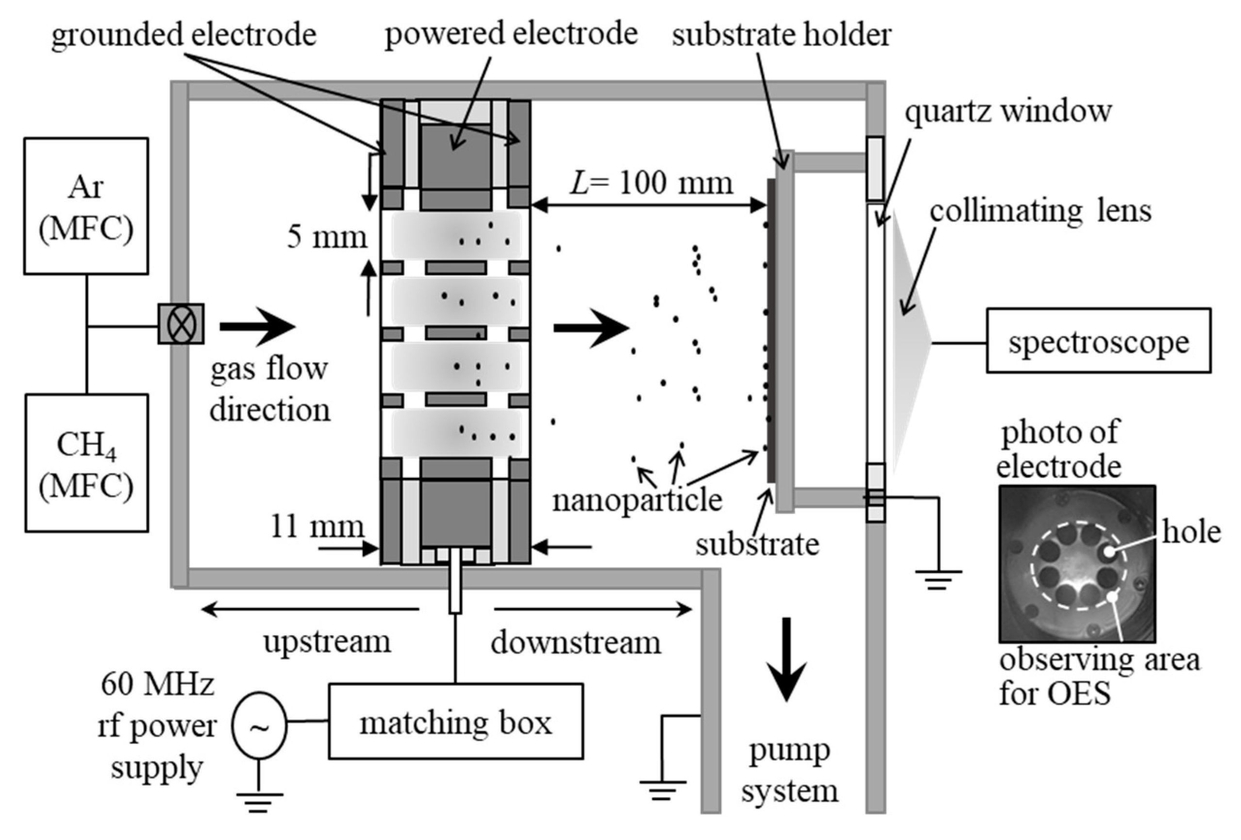
2. Materials and Methods

Figure 1 illustrates a schematic diagram of the MHDPCVD reactor [23,24]. Powered and grounded electrodes have 8 holes of 5 mm diameter. The powered electrode of 5 mm in thickness was a sandwich between two grounded electrodes of 1 mm in thickness. The gap between the powered and grounded electrode was 2 mm, and the total length of a hole was 11 mm. Ar and CH4 gases were introduced from the chamber’s left side, passed through the holes, and later evacuated by the pump system. The FR ratio of Ar and CH4 was 6:1. The total FR was controlled in a range of 10–120 sccm. During this process, gas pressure was kept at 266 Pa. The substrate holder was set at 100 mm apart from the electrode in the downstream region, and it was grounded. The powered electrode was connected to a 60 MHz radio frequency (rf) power supply through an impedance matching box. The discharge power and discharge period were 40 W and 90 min, respectively, and corresponding discharge and self-bias voltages were 230 and 80 V, respectively.
The CNPs generated in the discharges were collected by using mesh grids for a transmission electron microscope (TEM) and Si substrates for a Raman spectroscopy. The size and structure of CNPs were measured with TEM (JEOL, JEM-2010) and Raman spectroscope (Jasco, NRS3000; λ = 532 nm), respectively. Optical emission from plasmas discharges (all eight holes) was monitored by spectroscope (Ocean Optics, USB2000+) equipped with a collimating lens.

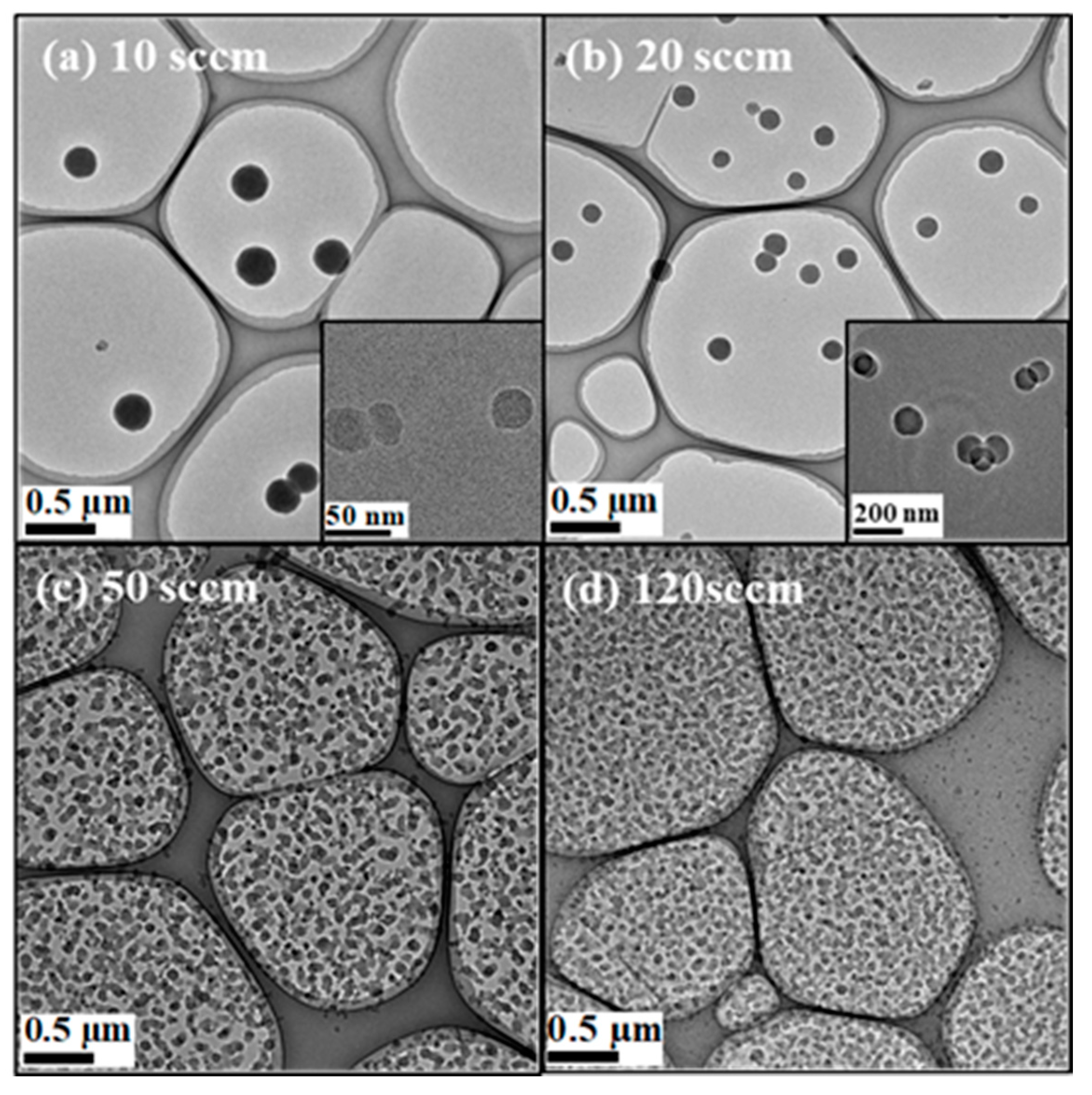
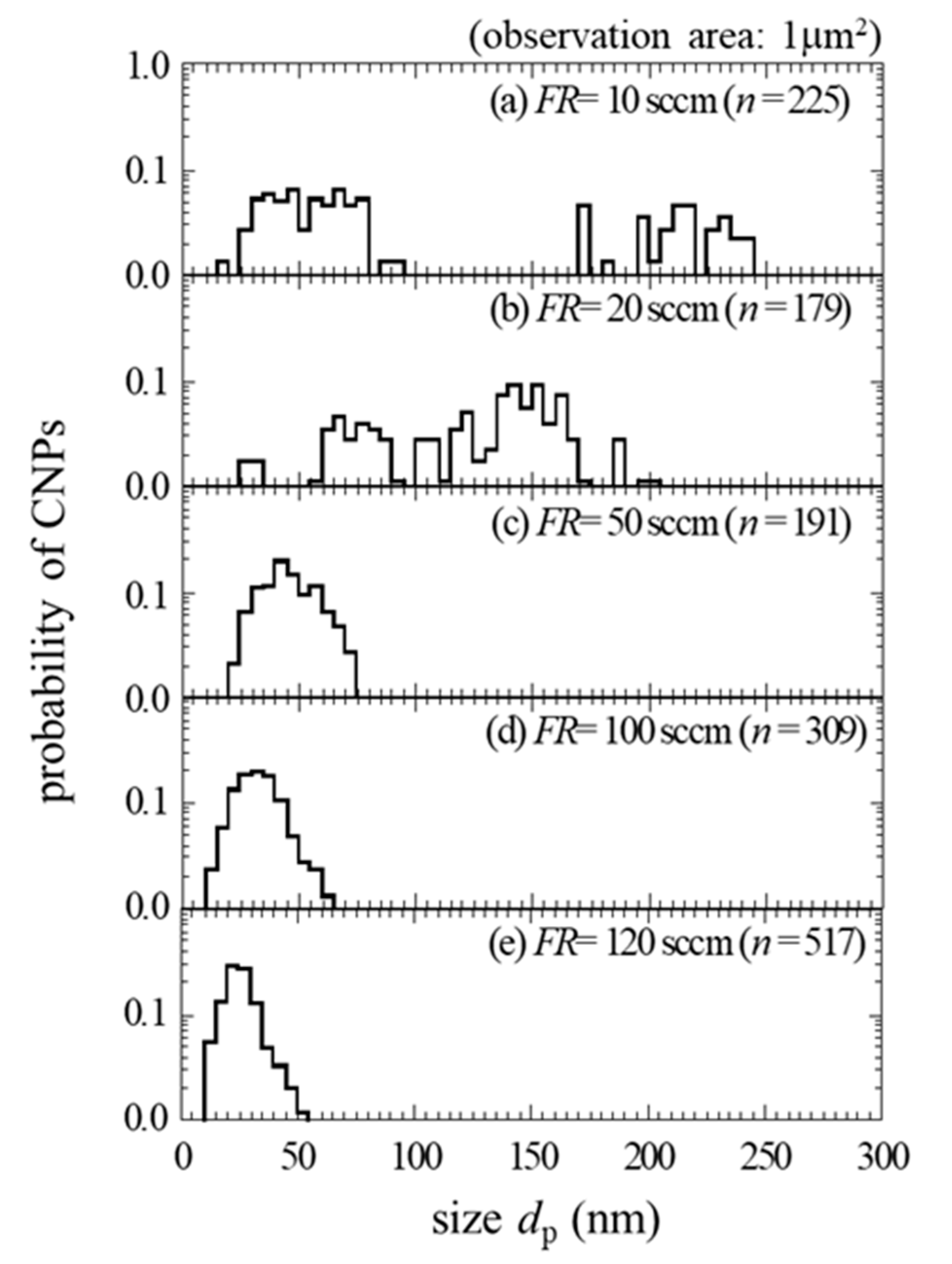
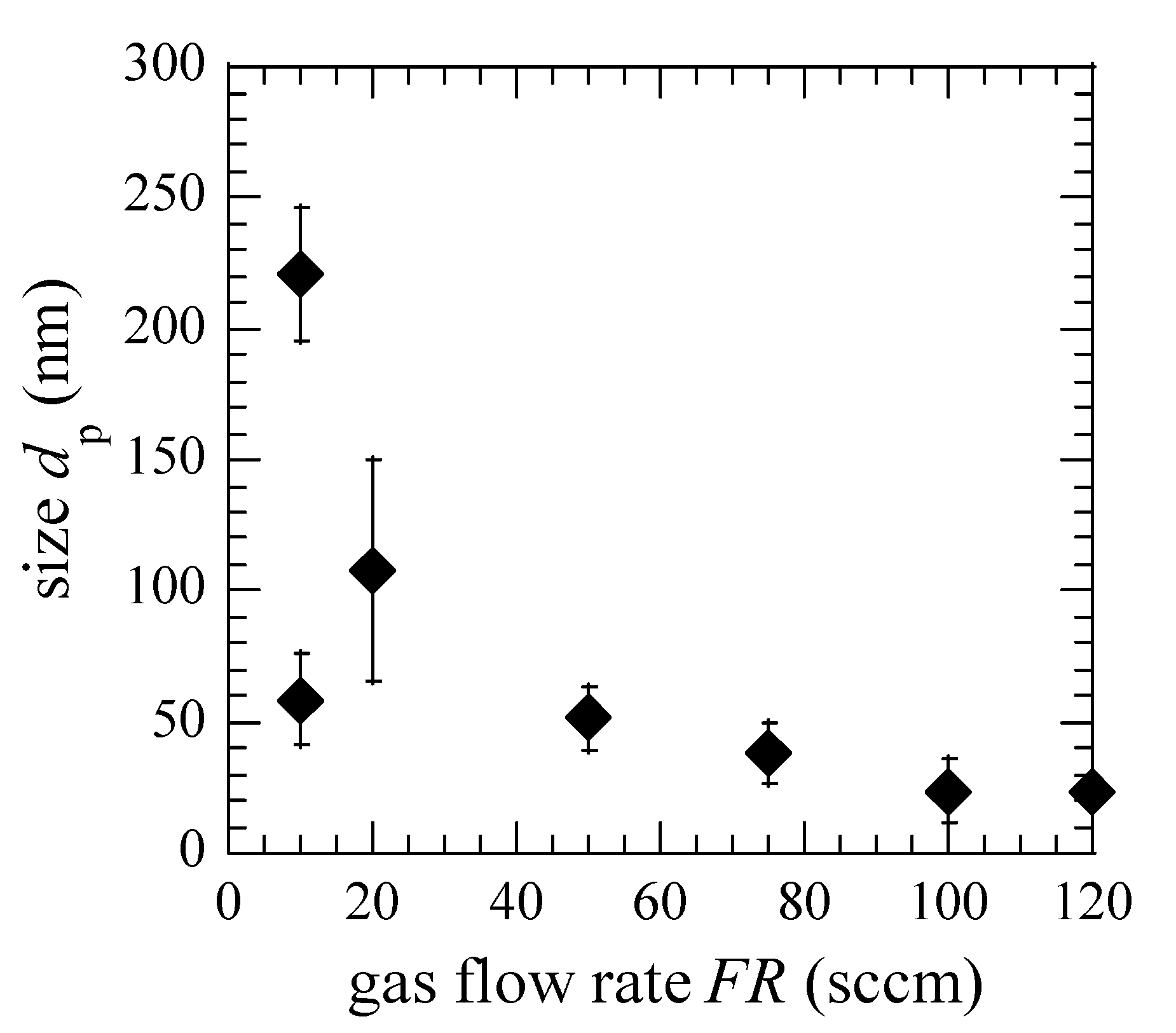
3. Results and Discussion

Figure 2a–d show the TEM images of CNPs as an FR parameter. With increasing FR, the mean size of CNPs decreased from approximately 220 nm at FR = 10 sccm to 25 nm at FR = 120 sccm. For FR = 10 sccm (Figure 2a) and FR = 20 sccm (Figure 2b), the CNPs deposit sparsely, while they deposit densely for FR = 50 sccm (Figure 2c) and FR = 120 sccm (Figure 2d). Additionally, the number of deposited CNPs increased with increasing FR. This shows the flux of CNPs increases with the increase in FR. Above 50 sccm, the deposited CNPs were stacked, then the absolute number of the deposited CNPs were unclear. Thus, we have evaluated the probability distribution of the CNPs for each FR.
Figure 3 shows the size distribution of the deposited CNPs obtained from TEM images where dp is the CNP size (diameter). The deposited nanoparticles were stacked for FR above 50 sccm. Thus, we estimated the probability of CNPs deposited on the mesh grid. Two group sizes were produced for FR = 10 sccm; (1) smaller group size has a size range between 20 and 90 nm, and (2) larger group size has a range between 170 and 250 nm. For FR = 20 sccm, two peaks at 60 and 150 nm were detected, but these peaks overlap and form one size group with a wide range between 30–200 nm. At the same time, one group size was obtained for FR above 50 sccm. Therefore, as the FR increases from 50 to 120 sccm, the peak size gradually shifts toward a smaller size from 45 to 20 nm, respectively. The size dispersion became narrower for higher FR from 50 and 120 sccm.
From the size distribution in Figure 3, we plotted a dependence of dp on FR, as shown in Figure 4. At FR below 20 sccm, the larger-sized nanoparticles seem to be separated from the smaller size group and grow in a monodisperse way. Similar growth behavior was observed for Si nanoparticles in silane plasmas in the earlier study [26]. Considering the larger size of CNPs at FR = 10 sccm, the dp decreases monotonically with increasing FR.
To obtain the structure of the CNPs, we have measured the XRD and Raman spectra of CNPs deposited at FR = 50 sccm. Figure 5 and Figure 6 show the XRD and Raman spectra, respectively. A broad peak in the XRD spectrum appears around 2θ = 20° and corresponds to the hydrogenated amorphous carbon (a-C:H) [27]. Figure 6 shows a Raman spectrum of nanoparticles deposited on the Si substrates at 50 sccm FR. Raman spectra clearly show the separated D (1350 cm−1), and G (1580 cm−1) bands. The area intensity ratio of D/G band was around 1.8; this indicates the structure of the CNPs were polymer like a-C:H [25,28,29,30]. Similar spectra were also observed at other FRs.
For the nanoparticle growth in the conventional CCP, the discharge duration is an essential factor. The size of nanoparticles increasing with an increase in CCP discharge duration [31]. The discharge duration was related to the period, which is the sum of the nucleation time and subsequent nucleated nanoparticles’ growth time. Continuous discharges sustained in holes and a low-density plasma penetrated the holes due to high working pressure of 266 Pa. The generated CNPs were transported inside the holes by the gas flow. The growth time of CNPs in the plasmas correlates with the gas residence time in holes. The gas residence time τres of holes corresponds to discharge duration in the conventional CCP. In this study, gas residence time was calculated from FR. For the CNP, growth involves two growth processes like the coagulation of CNPs during transport toward substrates and radical deposition on CNPs.
For the coagulation, CNPs are grown by the collision between two CNPs, as the volume of CNPs after the collision is the sum of two CNPs volume (before the collision). The size dp1 and number density np1 of CNPs after the collision are expressed by d p 1 = 2 1 3 d p 0 and n p 1 = n p 0 1 , respectively, where dp0 and np0 are the size and density of CNPs before the collision. To figure out the effects of the coagulation of CNPs, we examined the CNPs deposition at three positions in the transport region. Figure 7 shows the dependence of the size and surface density of deposited CNPs on the position L far from the electrode. For L = 100, 120, and 140 mm, the size is irrelevant to the position. The area density monotonically decreases with increasing L.
Previously, it was reported that the flux of CNPs proportionally increases with increasing the solid angle in the multi-hollow discharge plasma CVD method [24]. The solid angle is the main factor of decreased area density, see Figure 7. The results of the size and the area density indicate that the coagulation of CNPs was negligible. For the radical deposition, the growth rate Gr of CNP expressed as equation 1
G r = d d p d t = 2 D R r ,
where dp is the size (diameter) of CNPs and DRr is the deposition rate of radicals on CNPs. If we assume the sticking probability of radicals on CNPs is unity and carbon atoms are responsible for the mass of CNPs, the Gr is given by
G r = d d p d t = 2 ρ m C n r v thr ,
where ρ is the mass density of CNPs, mC the mass of a carbon atom (2.00 × 10⁻²⁶ kg), nr the number density of the radicals in plasmas, and vthr the thermal velocity of the radicals. The size and density of CNPs affect the radical density. The loss of radicals to the chamber wall is dominant if their size and density are low, while the loss to CNPs is prevalent if their size and density are high. The loss mode is determined by the coupling parameter Γ of CNPs in plasmas [32], given by the following equation.
Γ = 1 6 d p 2 n p 5 3 D w 3 ,
where Dw is the characteristic length of the reactor. For the Γ >> 1, the coupling among CNPs through radicals is strong, results in the deceased radical density with the time after the nucleation of CNPs. If the coupling is weak, the wall loss of radicals is dominant, resulting in no radical density change with the time. Further, to detect the Γ value, the np was deduced from the result in Figure 7.
Figure 7 shows the number of deposited CNPs per μm2 during the deposition time of 60 min. The flux of the CNPs can be calculated if the sticking probability of CNPs is unity. Considering the solid angle, the flux at the end of the holes deduced to be 1.30 × 1011 cm−2s−1. Raman results show that the structure of CNPs was polymer-like carbon, and the mass density of the CNPs was assumed 1.6 g/cm3. If the temperature of CNPs equal to that of the electrode (433 K), the np was 1.20 × 109 cm−3, and dp was 25 nm, as shown in Figure 6. Dw (Dw = 2.5 mm) assumed as the radius of hole, then Γ was 6.78 at the end of the discharge region. In the discharge region, the size of CNPs was smaller than 25 nm, and Γ value should be less than one. It suggests that the loss of radicals through the wall was predominant, which results in a constant rate of radical loss. To discuss the generation of the radicals, we have measured emission spectra in plasma. We measured two Ar I emission intensities at 425.9 nm I425.9 and 750.4 nm I750.4 with upper-level excitation energy of 14.7 eV (3p1) and 13.5 eV (2p1), respectively. These emission processes have little effect on quenching and radiation trapping. The upper excitation level has small cross sections for electron-impact excitation from metastable states [33,34]. The FR dependence of an emission intensity ratio I425.9/I750.4, shown in Figure 8. The ratio indicates the information of the high energy tail of the electron energy distribution, which relates to the radical generation.
Although the ratio is irrelevant to FR, as shown in Figure 8, the discharge voltage for each FR condition is almost the same, suggesting the electron density was irrelevant to the FR. These results indicate that the generation rate of radicals is unrelated to the FR.
In the steady state, the nr is proportional to the density of CH4 because the electron density and the loss rate of the radicals can be assumed to be constant based on the above discussion. Integrating Equation (2), the following formula gives the CNP size.
d p = 2 ρ k m C n CH 4 v thr t ,
where k is the ratio of generation rate and loss rate of radicals in the steady state, nCH4 the density of CH4, and t the interaction time of CNPs and radicals. The k value is related to the depletion rate of the CH4 molecules. In the current study, CNPs were nucleated in the discharge generated in the holes of the electrode. They grew in the discharge, transport with the gas flow, and growth was stopped outside the holes. We assumed that the growth of CNPs starts when the CH4 molecules enter into the holes where plasmas were generated. Thus, dp was assumed to be equal to zero at t = 0, and the growth of CNPs stops at t = τres. Figure 8 shows the dependence of dp on τres, based on FR dependence, together with the results reported earlier [23]. Considering the larger size of CNPs for FR = 10 sccm, the size of CNPs linearly increases with increasing the τres. In this study, nCH4 and vthr was 6.36 × 10²¹ m−3 and 8.24 × 10² m/s, respectively. The calculated value using Equation (4) as a parameter of k and the experimental results were well fitted for k = 0.035 (Figure 9). For the conventional CCP, the depletion rate of CH4 was about 3% for 1.33 Pa pure CH4 gas and 0.15 W/cm2 in discharge power density [35]. The depletion rate monotonically increases with CH4 pressure.
For the MHDPCVD, the discharge power density was 6.4 W/cm2, much higher than the conventional plasma CVD (above-mentioned), and the partial pressure of CH4 was 38 Pa. The radical loss to CNPs was small but cannot be ignored as it affects the Γ value. Thus, the fitted value of k is reasonable. Based on our results, the CNP in MHDPCVD was grown by the deposition of carbon-related radicals.

4. Conclusions

Through this work, we succeeded in synthesizing the size controlled CNPs using the Ar +CH4 MHDPCVD method continuously. The control range of the mean size was from 25 to 220 nm. We observed that size was proportional to the gas residence time in the discharges maintained in the electrode’s holes. We theoretically confirmed that CNPs were grown by the deposition of radicals during the discharges’ transport of CNPs, and CNPs move through gas flow in the discharges. The duration of the CNP transport in the discharge corresponds to the gas residence time. Therefore, the CNP size control using the MHDPVCD is a type of time of flight size control.

Author Contributions

Formal analysis, S.H.H. and Y.H.; writing—original draft preparation, S.H.H. and K.K. (Kazunori Koga); writing—review and editing, P.A., T.O., K.K. (Kunihiro Kamataki), N.I., M.S., J.-S.O., S.T. and T.N.; supervision, K.K. (Kazunori Koga), M.S. and T.N.; funding acquisition, K.K. (Kazunori Koga) and M.S. All authors have read and agreed to the published version of the manuscript.

Funding

This study was partly supported by JSPS KAKENHI Grant Number JP20H00142, JP20J13122 and JSPS Core-to-Core Program JPJSCCA2019002.

Institutional Review Board Statement

Not applicable.

Informed Consent Statement

Not applicable.

Data Availability Statements

Data is contained within the article.

Acknowledgments

This study was encouraged by Advanced Characterization Platform of the Nanotechnology Platform Japan sponsored by the Ministry of Education, Culture, Sports, Science and Technology (MEXT), Japan.

Conflicts of Interest

The authors declare no conflict of interest.

References

  1. Kumar, S.; Nehra, M.; Kedia, D.; Dilbaghi, N.; Tankeshwar, K.; Kim, K.H. Nanodiamonds: Emerging face of future nanotechnology. Carbon N. Y. 2019, 143, 678–699. [Google Scholar] [CrossRef]
  2. Li, S.; Pasc, A.; Fierro, V.; Celzard, A. Hollow carbon spheres, synthesis and applications-a review. J. Mater. Chem. A 2016, 4, 12686–12713. [Google Scholar] [CrossRef]
  3. Bian, X.; Chen, Q.; Zhang, Y.; Sang, L.; Tang, W. Deposition of nano-diamond-like carbon films by an atmospheric pressure plasma gun and diagnostic by optical emission spectrum on the process. Surf. Coat. Technol. 2008, 202, 5383–5385. [Google Scholar] [CrossRef]
  4. Tian, F.; He, C.N. Fabrication and growth mechanism of carbon nanospheres by chemical vapor deposition. Mater. Chem. Phys. 2010, 123, 351–355. [Google Scholar] [CrossRef]
  5. Wang, F.; Hong, R. Continuous preparation of structure-controlled carbon nanoparticle via arc plasma and the reinforcement of polymeric composites. Chem. Eng. J. 2017, 328, 1098–1111. [Google Scholar] [CrossRef]
  6. Estes, C.S.; Gerard, A.Y.; Godward, J.D.; Hayes, S.B.; Liles, S.H.; Shelton, J.L.; Stewart, T.S.; Webster, R.I.; Webster, H.F. Preparation of highly functionalized carbon nanoparticles using a one-step acid dehydration of glycerol. Carbon N. Y. 2019, 142, 547–557. [Google Scholar] [CrossRef]
  7. Li, Z.; Wang, L.; Li, Y.; Feng, Y.; Feng, W. Carbon-based functional nanomaterials: Preparation, properties and applications. Compos. Sci. Technol. 2019, 179, 10–40. [Google Scholar] [CrossRef]
  8. Kang, J.; Li, O.L.; Saito, N. Synthesis of structure-controlled carbon nano spheres by solution plasma process. Carbon N. Y. 2013, 60, 292–298. [Google Scholar] [CrossRef]
  9. Miao, J.Y.; Hwang, D.W.; Narasimhulu, K.V.; Lin, P.I.; Chen, Y.T.; Lin, S.H.; Hwang, L.P. Synthesis and properties of carbon nanospheres grown by CVD using Kaolin supported transition metal catalysts. Carbon N. Y. 2004, 42, 813–822. [Google Scholar] [CrossRef]
  10. Pottathara, Y.B.; Grohens, Y.; Kokol, V.; Kalarikkal, N.; Thomas, S. Synthesis and Processing of Emerging Two-Dimensional Nanomaterials; Elsevier Inc.: Amsterdam, The Netherlands, 2019; ISBN 9780128157510. [Google Scholar]
  11. Kumar, M.; Ando, Y. Chemical Vapor Deposition of Carbon Nanotubes: A Review on Growth Mechanism and Mass Production. J. Nanosci. Nanotechnol. 2010, 10, 3739–3758. [Google Scholar] [CrossRef] [Green Version]
  12. Koga, K.; Matsuoka, Y.; Tanaka, K.; Shiratani, M.; Watanabe, Y. In situ observation of nucleation and subsequent growth of clusters in silane radio frequency discharges. Appl. Phys. Lett. 2000, 77, 196–198. [Google Scholar] [CrossRef]
  13. Nunomura, S.; Shiratani, M.; Koga, K.; Kondo, M.; Watanabe, Y. Nanoparticle coagulation in fractionally charged and charge fluctuating dusty plasmas. Phys. Plasmas 2008, 15, 080703. [Google Scholar] [CrossRef]
  14. Kim, K.; Park, J.H.; Doo, S.G.; Nam, J.D.; Kim, T. Generation of size and structure controlled Si nanoparticles using pulse plasma for energy devices. Thin Solid Films 2009, 517, 4184–4187. [Google Scholar] [CrossRef]
  15. Nakamura, W.M.; Shimokawa, D.; Miyahara, H.; Koga, K.; Shiratani, M. Spatial Profile of Deposition Rate of a-Si:H Films in Multi-Hollow Discharge Plasma Chemical Vapor Deposition. Trans. Mater. Res. Soc. Jpn. 2007, 32, 469–472. [Google Scholar] [CrossRef]
  16. Shiratani, M.; Koga, K.; Iwashita, S.; Uchida, G.; Itagaki, N.; Kamataki, K. Nano-factories in plasma: Present status and outlook. J. Phys. D Appl. Phys. 2011, 44, 1–8. [Google Scholar] [CrossRef]
  17. Koga, K.; Nakahara, K.; Kim, Y.-W.; Kawashima, Y.; Matsunaga, T.; Sato, M.; Yamashita, D.; Matsuzaki, H.; Uchida, G.; Kamataki, K.; et al. Deposition of cluster-free P-doped a-Si:H films using SiH4+PH3 multi-hollow discharge plasma CVD. Phys. Status Solidi 2011, 8, 3013–3016. [Google Scholar] [CrossRef]
  18. Uchida, G.; Yamamoto, K.; Kawashima, Y.; Sato, M.; Nakahara, K.; Kamataki, K.; Itagaki, N.; Koga, K.; Kondo, M.; Shiratani, M. Surface nitridation of silicon nano-particles using double multi-hollow discharge plasma CVD. Phys. Status Solidi Curr. Top. Solid State Phys. 2011, 8, 3017–3020. [Google Scholar] [CrossRef]
  19. Koga, K.; Matsunaga, T.; Kim, Y.; Nakahara, K.; Yamashita, D.; Matsuzaki, H.; Kamataki, K.; Uchida, G.; Itagaki, N.; Shiratani, M. Combinatorial deposition of microcrystalline silicon films using multihollow discharge plasma chemical vapor deposition. Jpn. J. Appl. Phys. 2012, 51, 1–4. [Google Scholar] [CrossRef]
  20. Kim, Y.; Matsunaga, T.; Nakahara, K.; Seo, H.; Kamataki, K.; Uchida, G.; Itagaki, N.; Koga, K.; Shiratani, M. Effects of nanoparticle incorporation on properties of microcrystalline films deposited using multi-hollow discharge plasma CVD. Surf. Coat. Technol. 2013, 228, S550–S553. [Google Scholar] [CrossRef]
  21. Seo, H.; Ichida, D.; Hashimoto, S.; Itagaki, N.; Koga, K.; Shiratani, M.; Nam, S.H.; Boo, J.H. Improvement of charge transportation in Si quantum dot-sensitized solar cells using vanadium doped TiO2. J. Nanosci. Nanotechnol. 2016, 16, 4875–4879. [Google Scholar] [CrossRef]
  22. Toko, S.; Kanemitsu, Y.; Seo, H.; Itagaki, N.; Koga, K.; Shiratani, M. Optical bandgap energy of Si nanoparticle composite films deposited by a multi-hollow discharge plasma chemical vapor deposition method. J. Nanosci. Nanotechnol. 2016, 16, 10753–10757. [Google Scholar] [CrossRef]
  23. Hwang, S.H.; Kamataki, K.; Itagaki, N.; Koga, K.; Shiratani, M. Effects of gas pressure on the size distribution and structure of carbon nanoparticles using Ar + CH4 multi-hollow discharged plasma chemical vapor deposition. Plasma Fusion Res. 2019, 14, 1–5. [Google Scholar] [CrossRef] [Green Version]
  24. Hwang, S.H.; Okumura, T.; Kamataki, K.; Itagaki, N.; Koga, K.; Shiratani, M. Size and Flux of Carbon Nanoparticles Synthesized by Ar+CH4 Multi-hollow Plasma Chemical Vapor Deposition. Diam. Relat. Mater. 2020, 108050. [Google Scholar] [CrossRef]
  25. Hwang, S.H.; Okumura, T.; Kamataki, K.; Itagaki, N.; Koga, K.; Nakatani, T.; Shiratani, M. Low stress diamond-like carbon films containing carbon nanoparticles fabricated by combining rf sputtering and plasma chemical vapor deposition. Jpn. J. Appl. Phys. 2020, 59, 100906. [Google Scholar] [CrossRef]
  26. Watanabe, Y. Formation and behaviour of nano/micro-particles in low pressure plasmas. J. Phys. D Appl. Phys. 2006, 39, R329. [Google Scholar] [CrossRef]
  27. Siddique, A.B.; Pramanick, A.K.; Chatterjee, S.; Ray, M. Amorphous Carbon Dots and their Remarkable Ability to Detect 2,4,6-Trinitrophenol. Sci. Rep. 2018, 8, 9700. [Google Scholar] [CrossRef]
  28. Ferrari, A.C.; Robertson, J. Raman spectroscopy of amorphous, nanostructured, diamond like carbon, and nanodiamond. Philos. Trans. R. Soc. Lond. A 2004, 362, 2477–2512. [Google Scholar] [CrossRef]
  29. Merlen, A.; Buijnsters, J.G.; Pardanaud, C. A guide to and review of the use of multiwavelength Raman spectroscopy for characterizing defective aromatic carbon solids: From graphene to amorphous carbons. Coatings 2017, 7, 153. [Google Scholar] [CrossRef]
  30. Dong, X.; Koga, K.; Yamashita, D.; Seo, H.; Itagaki, N.; Shiratani, M.; Setsuhara, Y.; Sekine, M.; Hori, M. Effects of deposition rate and ion bombardment on properties of a-C:H films deposited by H-assisted plasma CVD method. Jpn. J. Appl. Phys. 2016, 55. [Google Scholar] [CrossRef]
  31. Nunomura, S.; Kita, M.; Koga, K.; Shiratani, M.; Watanabe, Y. In situ simple method for measuring size and density of nanoparticles in reactive plasmas. J. Appl. Phys. 2006, 99, 083302. [Google Scholar] [CrossRef]
  32. Shiratani, M.; Koga, K.; Kamataki, K.; Iwashita, S. Theory for correlation between plasma fluctuation and fluctuation of nanoparticle growth in reactive plasmas Theory for correlation between plasma fl uctuation and fl uctuation of nanoparticle growth in reactive plasmas. Jpn. J. Appl. Phys. 2014, 53, 010201. [Google Scholar] [CrossRef] [Green Version]
  33. Moshkalyov, S.A. Deposition of silicon nitride by low-pressure electron cyclotron resonance plasma enhanced chemical vapor deposition in N2/Ar/SiH4. J. Vac. Sci. Technol. B Microelectron. Nanom. Struct. 1997, 15, 2682. [Google Scholar] [CrossRef]
  34. Daltrini, A.M.; Moshkalev, S.A.; Monteiro, M.J.R.; Besseler, E.; Kostryukov, A.; Machida, M. Mode transitions and hysteresis in inductively coupled plasmas. J. Appl. Phys. 2007, 101, 073309. [Google Scholar] [CrossRef] [Green Version]
  35. Toyoda, H.; Kojima, H.; Sugai, H. Mass spectroscopic investigation of the CH3 radicals in a methane rf discharge. Appl. Phys. Lett. 1989, 54, 1507–1509. [Google Scholar] [CrossRef]
Figure 1. Multi-hollow discharge plasma.
Processes 09 00002 g001
Figure 2. TEM images of carbon nanoparticles produced for (a) FR = 10 sccm, (b) FR = 20 sccm, (c) FR = 50 sccm, and (d) FR = 120 sccm. Insets in (a) and (b) show their high magnification TEM images.
Processes 09 00002 g002
Figure 3. The size distribution of CNPs as a parameter of FR where n is the number of measured CNPs.
Processes 09 00002 g003
Figure 4. Dependence of dp on FR. Error bar shows the standard deviation.
Processes 09 00002 g004
Figure 5. XRD spectrum of CNPs for FR = 50 sccm.
Processes 09 00002 g005
Figure 6. Raman spectrum of CNPs for FR = 50 sccm.
Processes 09 00002 g006
Figure 7. Dependence of the size and surface density of deposited CNPs on the position L far from the electrode for FR = 100 sccm. Error bar shows the standard deviation.
Processes 09 00002 g007
Figure 8. Dependence of I425.9/I750.4 on FR.
Processes 09 00002 g008
Figure 9. Dependence of dp on τres. Open circles indicate the results reported earlier [23]. Lines were obtained by Equation (4). Error bar shows the standard deviation.
Processes 09 00002 g009
Publisher’s Note: MDPI stays neutral with regard to jurisdictional claims in published maps and institutional affiliations.

