Investigation of the Thermal Properties of Electrodes on the Film and Its Heating Behavior Induced by Microwave Irradiation in Mounting Processes


Abstract
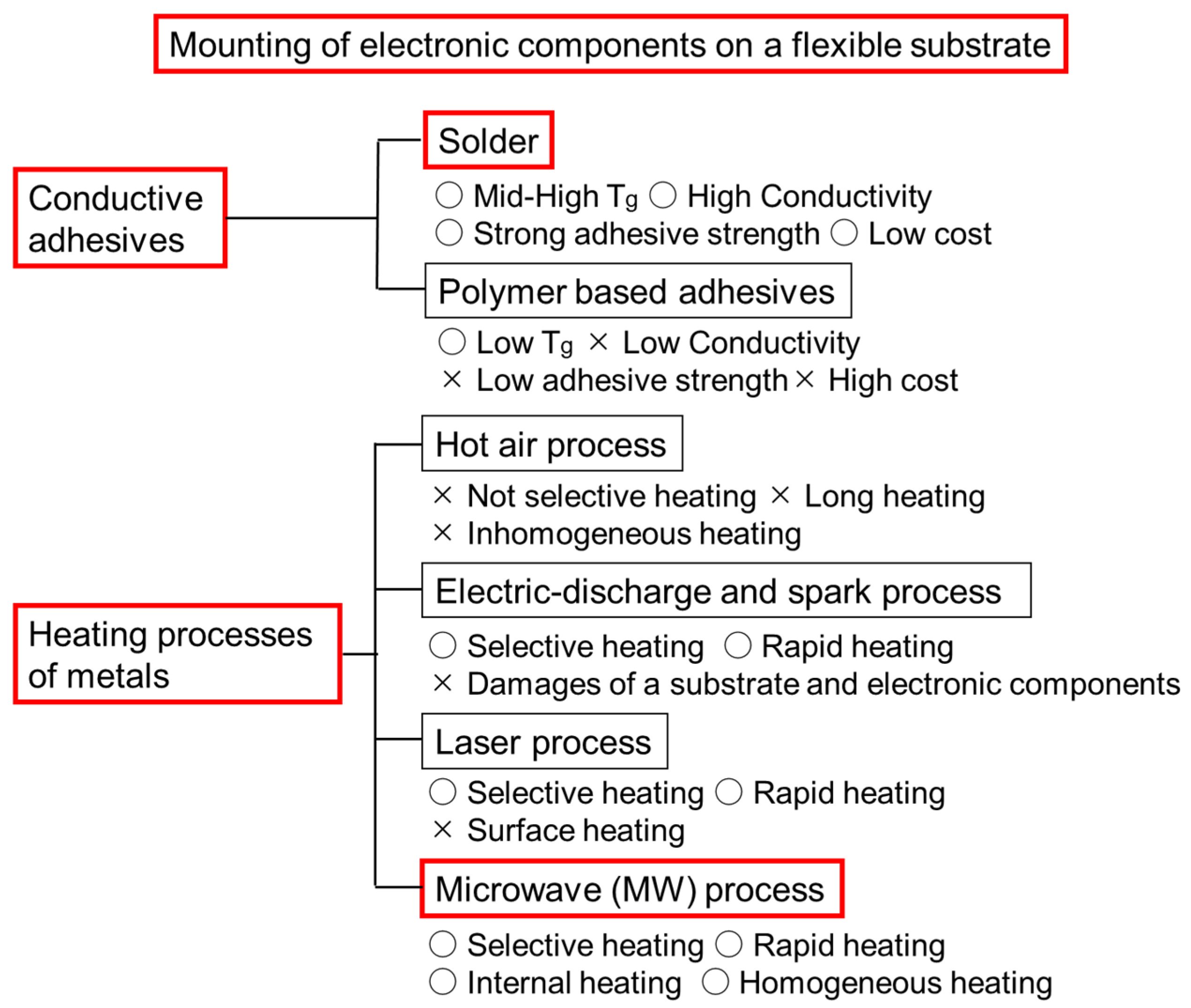
1. Introduction
2. Experimental Section
2.1. Materials
2.2. Preparation of Samples and the Induction Soldering Method by MW
2.2.1. Preparation of Silver Paste Pad for the Investigation of the Pad Shape on Induction Soldering by MW and the Induction Soldering Method by MW
2.2.2. Preparation of Samples for Investigation of Solder Heating Behavior by the Induction Soldering of MW and Induction Soldering by MW
2.2.3. Preparation of Samples for Mounting Electric Components by the Induction Soldering of MW and Induction Soldering by MW
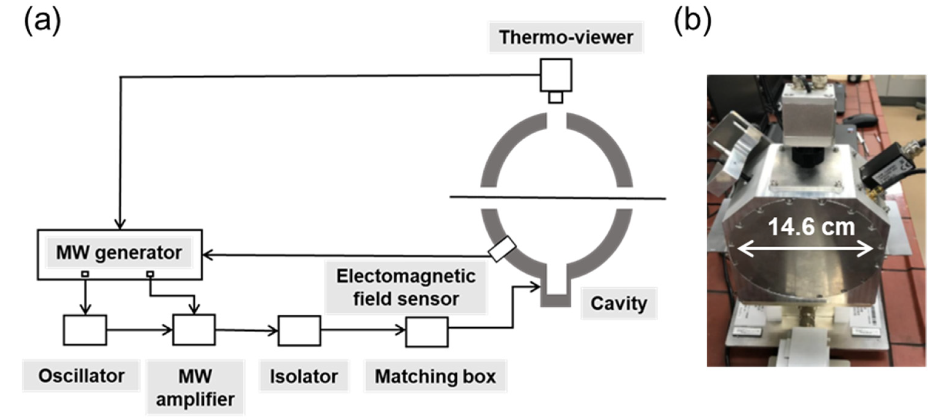
2.3. MW Sintering System
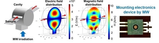
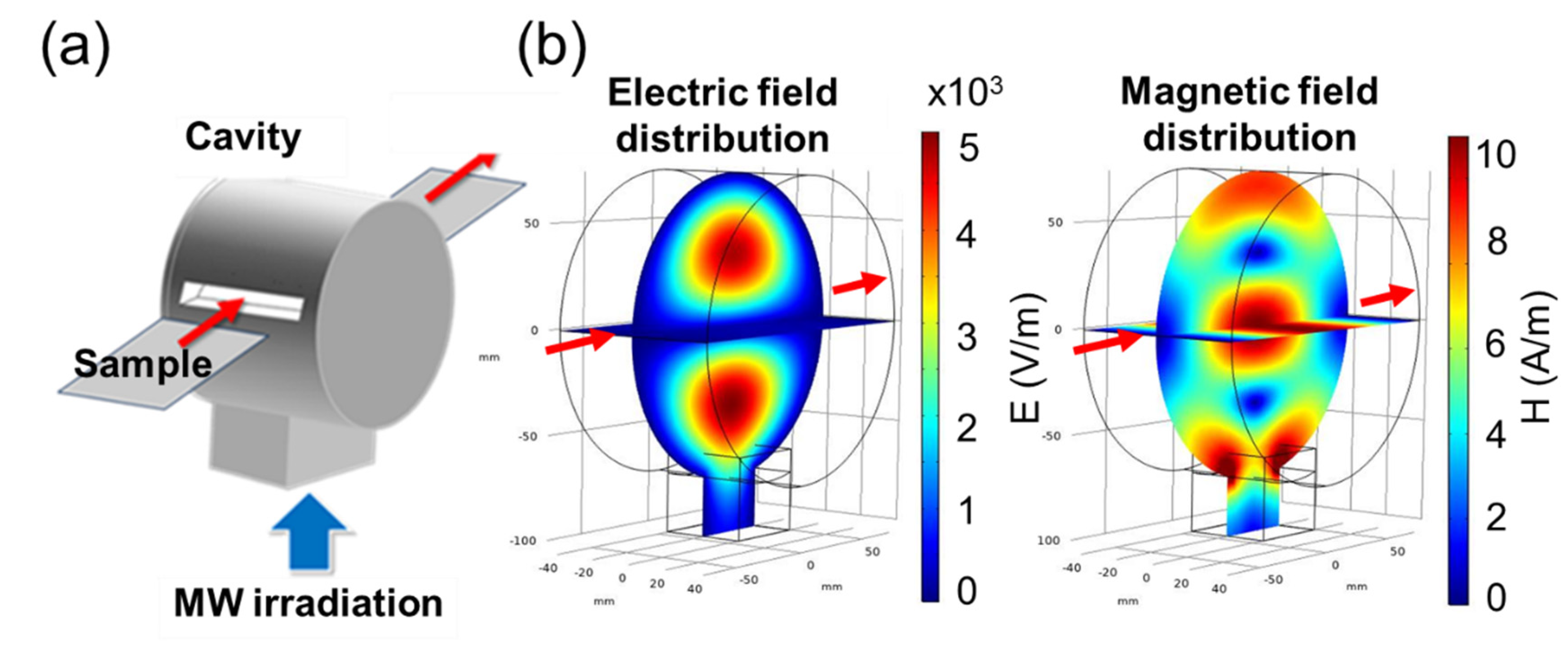
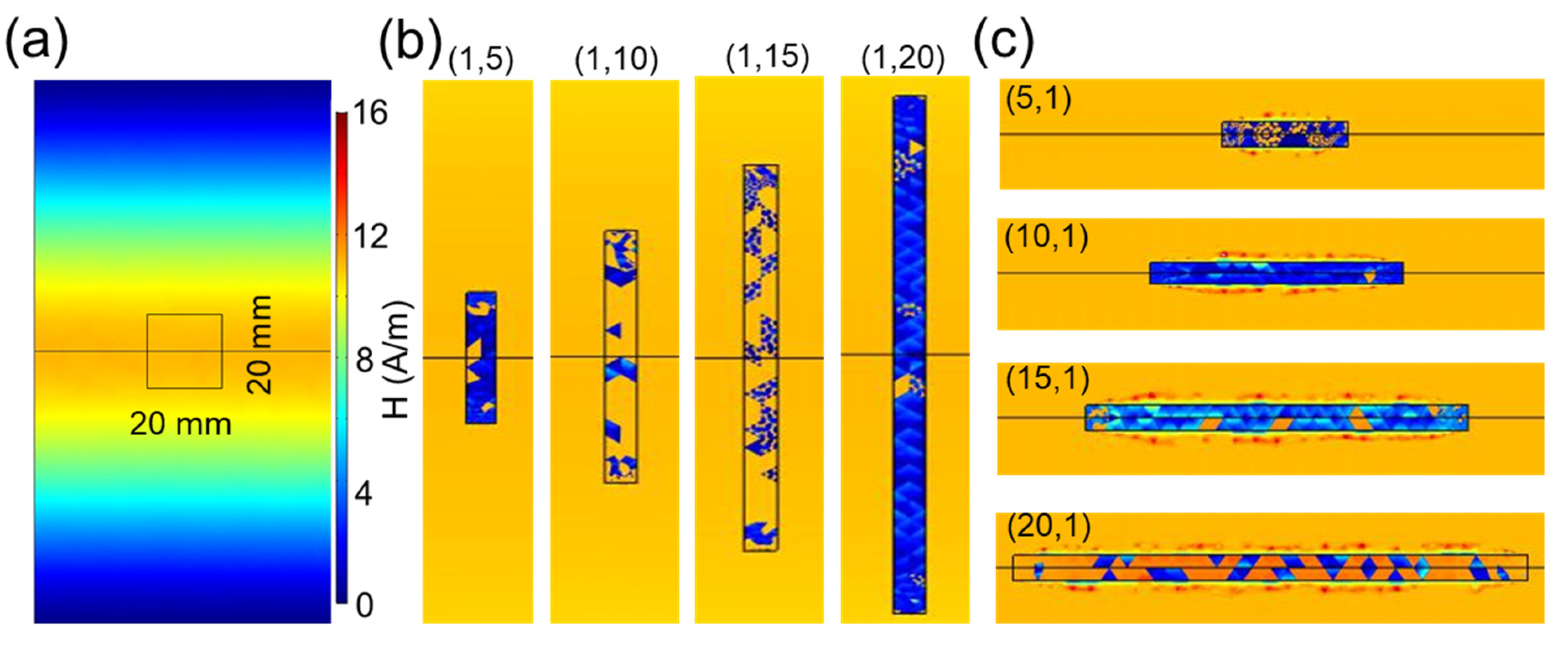
2.4. Electromagnetic Simulation in TM110 Mode Cavity with and without Bulk Silver
2.5. Instruments
2.6. Method of Measuring Room Temperature
3. Results and Discussion
3.1. Induction Soldering System by MW
3.2. MW Sintering Properties and Morphology of Solder Paste
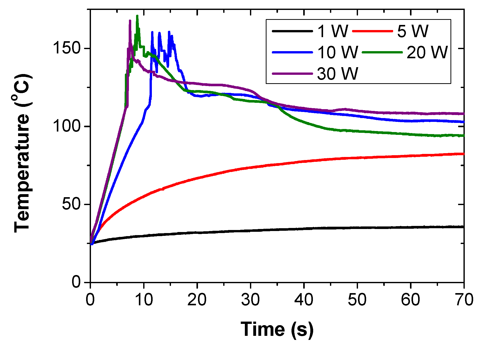
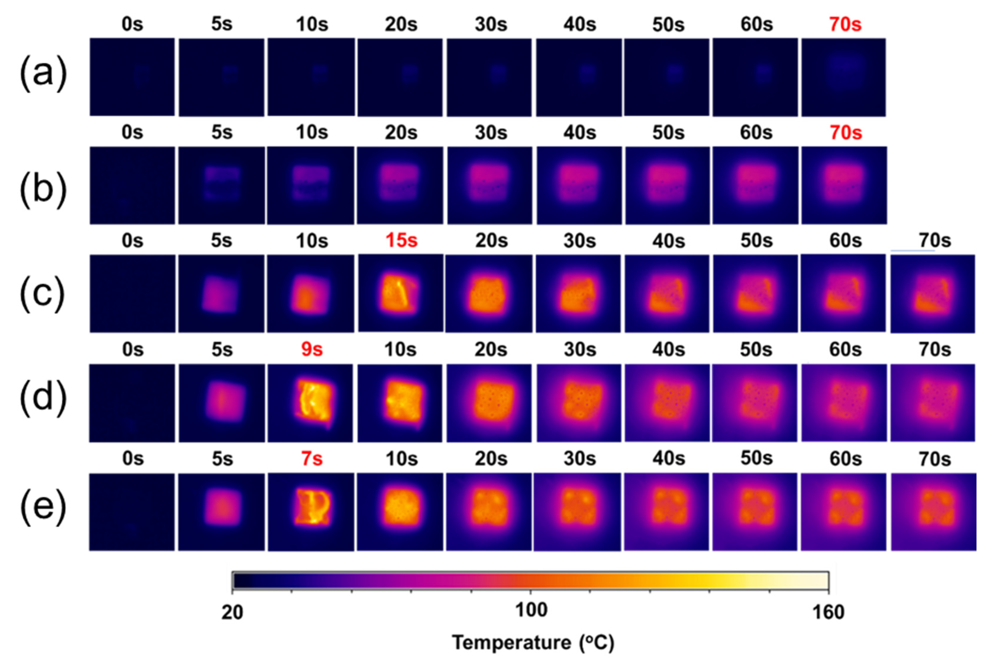
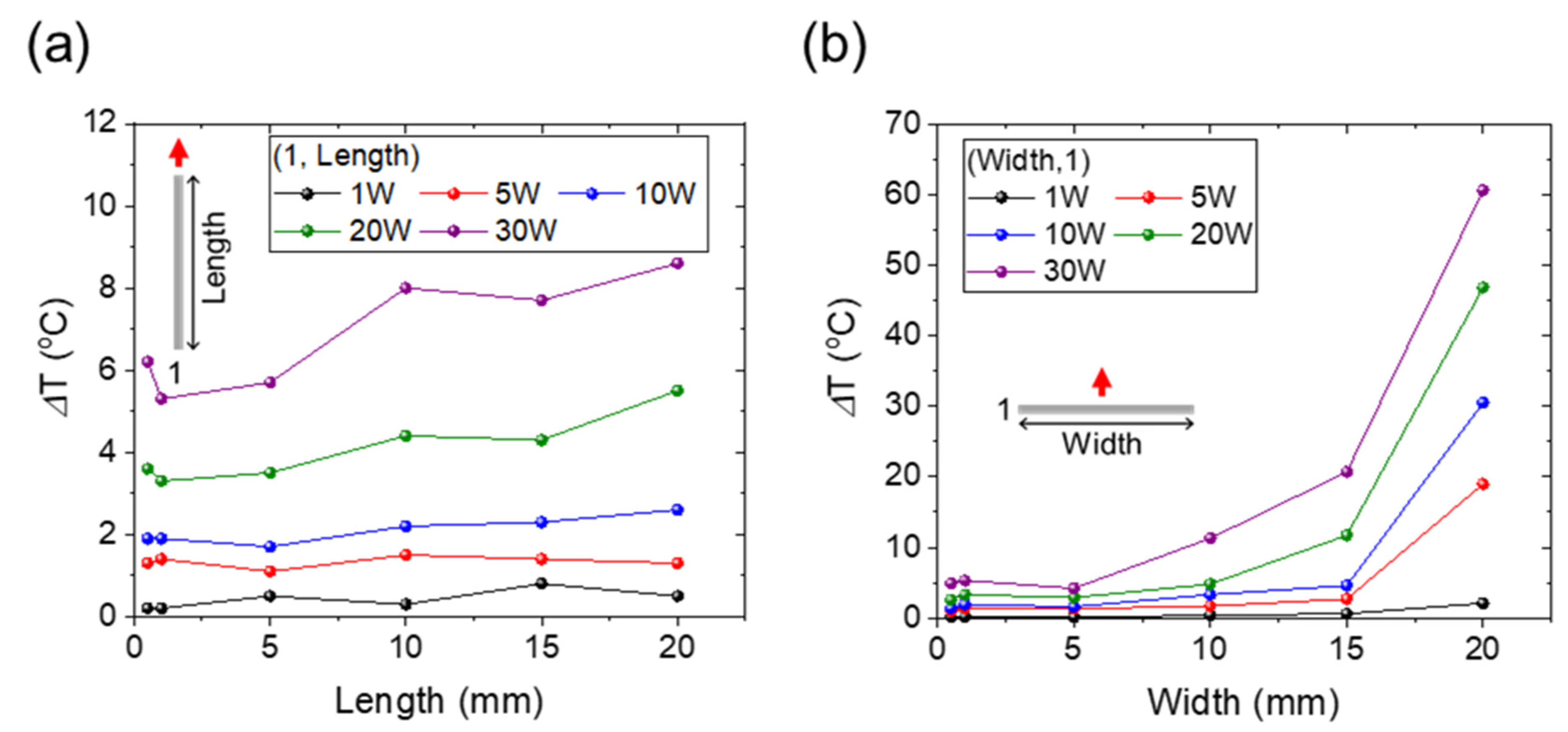
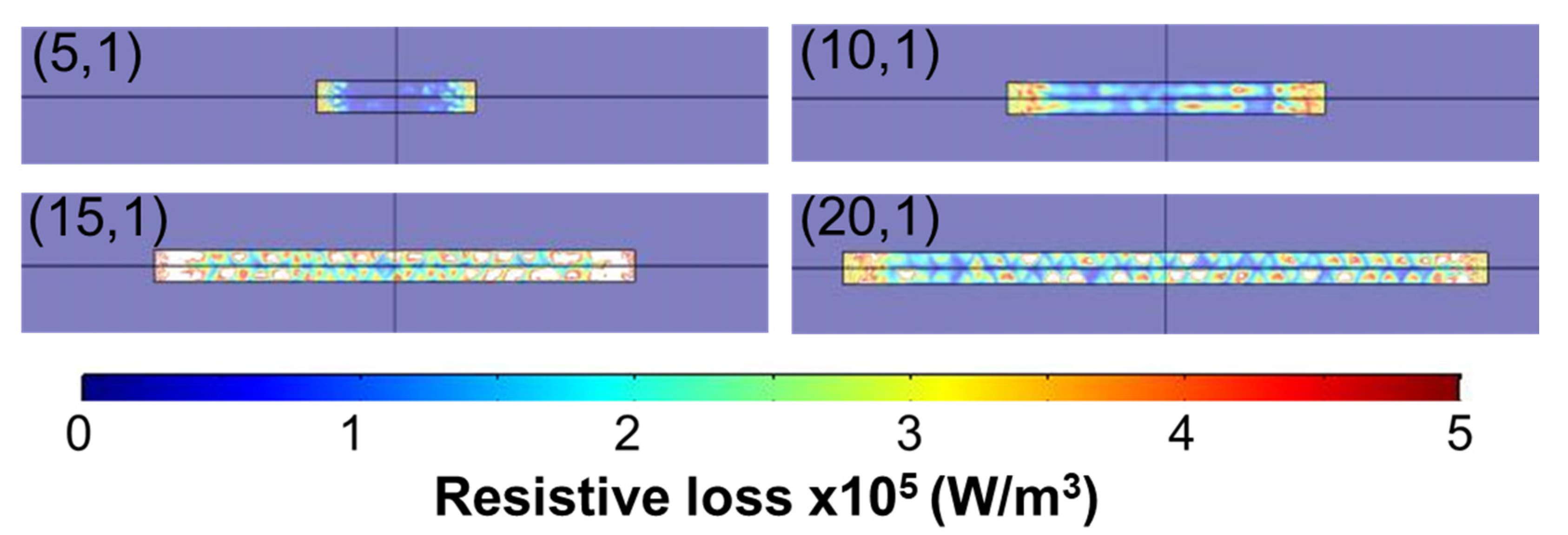
3.3. Thermal Property of Silver Pad Patterns by the Induction Soldering of MW
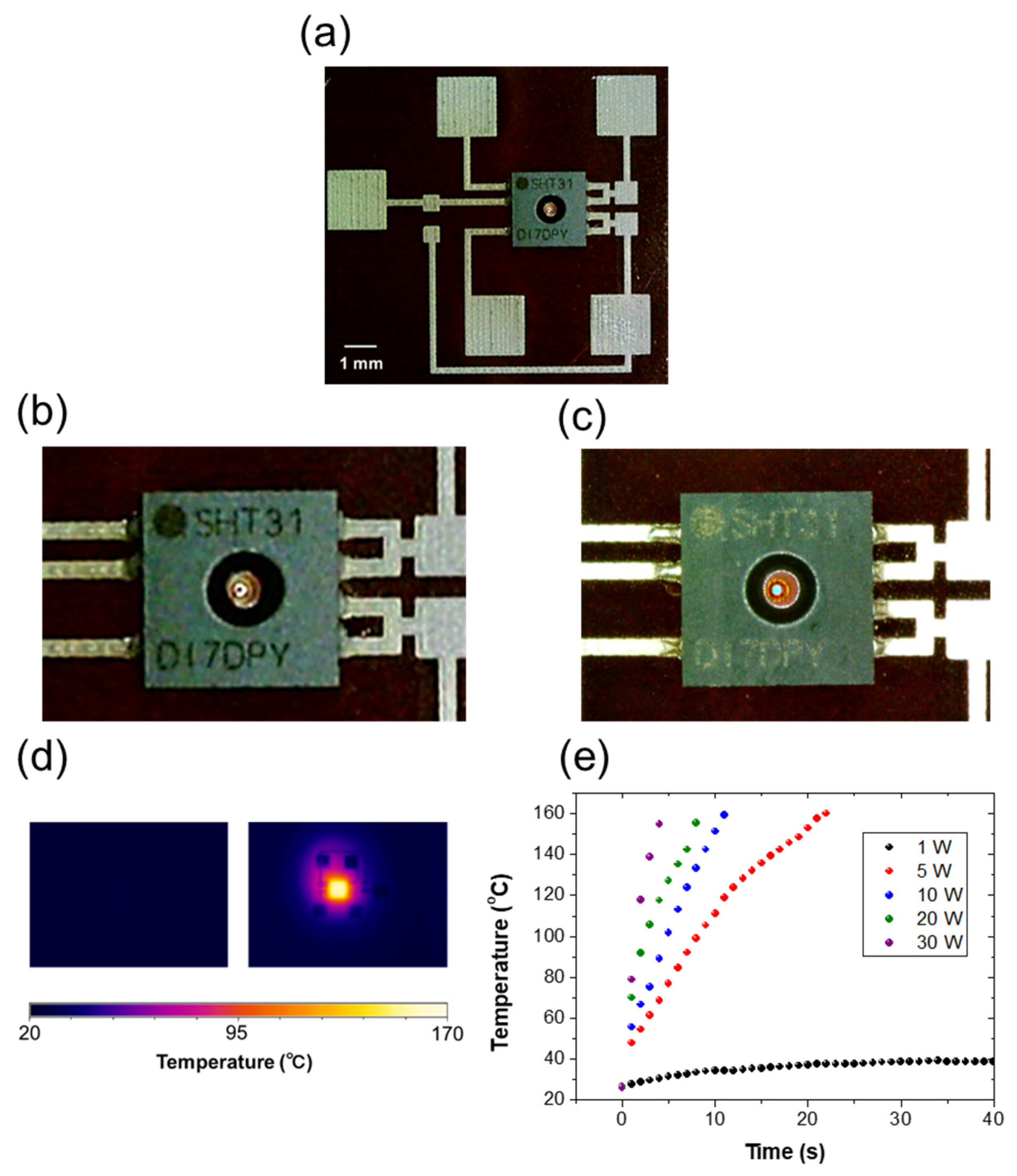
3.4. Mounting a Device on a Polyimide Sheet Using the MW Method
4. Conclusions
Supplementary Materials
Author Contributions
Funding
Conflicts of Interest
References
- Alaa, M.; Zaidan, A.; Zaidan, B.; Talal, M.; Kiah, M. A review of smart home applications based on Internet of Things. J. Netw. Comput. Appl. 2017, 97, 48–65. [Google Scholar] [CrossRef]
- Liu, Y.; Wang, H.; Zhao, W.; Zhang, M.; Qin, H.; Xie, Y. Flexible, Stretchable Sensors for Wearable Health Monitoring: Sensing Mechanisms, Materials, Fabrication Strategies and Features. Sensors 2018, 18, 645. [Google Scholar] [CrossRef] [PubMed]
- Parrilla, M.; Cuartero, M.; Crespo, G.A. Wearable potentiometric ion sensors. TrAC Trebds Anal. Chem. 2019, 110, 303–320. [Google Scholar] [CrossRef]
- Acome, E.; Mitchell, S.K.; Morrissey, T.G.; Emmett, M.B.; Benjamin, C.; King, M.; Radakovitz, M.; Keplinger, C. Hydraulically amplified self-healing electrostatic actuators with muscle-like performance. Science 2018, 359, 61–65. [Google Scholar] [CrossRef] [PubMed]
- Ammar, M.; Russello, G.; Crispo, B. Internet of Things: A survey on the security of IoT frameworks. J. Inf. Secur. Appl. 2018, 38, 8–27. [Google Scholar] [CrossRef]
- Pan, J.; McEIhannon, J. Future Edge Cloud and Edge Computing for Internet of Things Applications. IEEE Internet Things J. 2018, 5, 439–449. [Google Scholar] [CrossRef]
- Abtew, M.; Selvaduray, G. Lead-free solders in microelectronics. Mater. Sci. Eng. Rep. 2000, 27, 95–141. [Google Scholar] [CrossRef]
- Suganuma, K.; Kim, S.J.; Kim, K.S. High-temperature lead-free solders: Properties and possibilities. JOM 2009, 61, 64–71. [Google Scholar] [CrossRef]
- Li, Y.; Wong, C.P. Recent advances of conductive adhesives as a lead-free alternative in electronic packaging: Materials, processing, reliability and applications. Mater. Sci. Eng. R 2006, 51, 1–35. [Google Scholar] [CrossRef]
- Santos, E.C.; Shiomi, M.; Osakada, K.; Laoui, T. Rapid manufacturing of metal components by laser forming. Int. J. Mach. Tools Manuf. 2006, 46, 1459–1468. [Google Scholar] [CrossRef]
- Gu, D.D.; Meiners, W.; Wissenbach, K.; Poprawe, R. Laser additive manufacturing of metallic components: Materials, processes and mechanisms. Int. Mater. Rev. 2012, 57, 133–164. [Google Scholar] [CrossRef]
- Lee, W.H.; Seong, J.G.; Yoon, Y.H.; Jeong, C.H.; Van Tyne, C.J.; Lee, H.G.; Chang, S.Y. Synthesis of TiC reinforced Ti matrix composites by spark plasma sintering and electric discharge sintering; a comparative assessment of microstructural and mechanical properties. Ceram. Int. 2019, 45, 8108–8114. [Google Scholar] [CrossRef]
- Mishra, R.R.; Sharma, A.K. Microwave-material interaction phenomena: Heating mechanisms, challenges and opportunities in material processing. Compos. Part A 2016, 81, 78–97. [Google Scholar] [CrossRef]
- Khaled, D.E.; Novas, N.; Gazquez, J.A.; Manzano-Agugliaro, F. Microwave dielectric heating: Applications on metals processing. Renew. Sustain. Energ. Rev. 2018, 82, 2880–2892. [Google Scholar] [CrossRef]
- Zou, Y.; Li, C.H.; Liu, J.A.; Wu, J.M.; Hu, L.; Gui, R.F.; Shi, Y.S. Towards fabrication of high-performance Al2O3 ceramics by indirect selective laser sintering based on particle packing optimization. Ceram. Int. 2019, 45, 12654–12662. [Google Scholar] [CrossRef]
- Chaim, R.; Levin, M.; Shlayer, A.; Estournes, C. Sintering and densification of nanocrystalline ceramic oxide powders: A review. Adv. Appl. Ceram. 2008, 107, 159–169. [Google Scholar] [CrossRef]
- Mirzaei, A.; Neri, G. Microwave-assisted synthesis of metal oxide nanostructures for gas sensing application: A review. Sens. Actuators B Chem. 2016, 237, 749–775. [Google Scholar] [CrossRef]
- Loharkar, P.K.; Ingle, A.; Jhavar, S. Parametric review of microwave-based materials processing and its applications. J. Mater. Res. Technol. 2019, 8, 3306–3326. [Google Scholar] [CrossRef]
- Levin, E.E.; Grebenkemper, J.H.; Pollock, T.M.; Seshadri, R. Protocols for High Temperature Assisted-Microwave Preparation of Inorganic Compounds. Chem. Mater. 2019, 31, 7151–7159. [Google Scholar] [CrossRef]
- Thomas-Hillman, I.; Laybourn, A.; Dodds, C.; Kingman, S.W. Realising the environmental benefits of metal–organic frameworks: Recent advances in microwave synthesis. J. Mater. Chem. A 2018, 6, 11564–11581. [Google Scholar] [CrossRef]
- Horikoshi, S.; Osawa, A.; Abe, M.; Serpone, N. On the generation of hot-spots by microwave electric and magnetic fields and their impact on a microwave-assisted reaction in the presence of metallic Pd nanoparticles on an activated carbon support. J. Phys. Chem. C 2011, 115, 23030–23035. [Google Scholar] [CrossRef]
- Nishioka, M.; Miyakawa, M.; Kataoka, H.; Koda, H.; Sato, K.; Suzuki, T.M. Continuous synthesis of monodispersed silver nanoparticles using a homogeneous heating microwave reactor system. Nanoscale 2011, 3, 2621–2626. [Google Scholar] [CrossRef] [PubMed]
- Miyakawa, M.; Hiyoshi, N.; Koda, H.; Watanabe, K.; Kunigami, H.; Kunigami, H.; Miyazawa, A.; Nishioka, M. Continuous syntheses of carbon-supported Pd and Pd@Pt core-shell nanoparticles using a flow-type single-mode microwave reactor. RSC Adv. 2020, 10, 6571–6575. [Google Scholar] [CrossRef]
- Morgan, S.P., Jr. Effect of surface roughness on eddy current losses at microwave frequencies. J. Appl. Pnys. 1949, 20, 352–362. [Google Scholar] [CrossRef]
- Webb, A. Cavity- and waveguide-resonators in electron paramagnetic resonance, nuclear magnetic resonance, and magnetic resonance imaging. Prog. Nucl. Magn. Reson. Spectrosc. 2014, 83, 1–20. [Google Scholar] [CrossRef]
- Verhoeven, W.; van Rens, J.F.M.; Kemper, A.H.; Rietman, E.H.; van Doorn, H.A.; Koole, I.E.; Kieft, R.; Mutsaers, P.H.A.; Luiten, O.J. Design and characterization of dielectric filled TM110 micraowave cavities for ultrafast electron microscopy. Rev. Sci. Instrum. 2019, 90, 080370. [Google Scholar] [CrossRef]
- Cao, Z.; Yoshikawa, N.; Taniguchi, S. Directional selectivity of microwave H field heating of Au thin films and non-doped Si plates. Mater. Chem. Phys. 2009, 117, 14–17. [Google Scholar] [CrossRef]


| Temperature Sensor | Voltage (V) | Temperature b (°C) |
|---|---|---|
| Digital meter | - | 23.4 |
| SHTDA-2 | 1.6158 | 24.6 |
| SHT-31-DIS-B a | 1.6210 | 24.8 |
© 2020 by the authors. Licensee MDPI, Basel, Switzerland. This article is an open access article distributed under the terms and conditions of the Creative Commons Attribution (CC BY) license (http://creativecommons.org/licenses/by/4.0/).
Share and Cite
Kanazawa, K.; Nakamura, T.; Nishioka, M.; Uemura, S. Investigation of the Thermal Properties of Electrodes on the Film and Its Heating Behavior Induced by Microwave Irradiation in Mounting Processes. Processes 2020, 8, 557. https://doi.org/10.3390/pr8050557
Kanazawa K, Nakamura T, Nishioka M, Uemura S. Investigation of the Thermal Properties of Electrodes on the Film and Its Heating Behavior Induced by Microwave Irradiation in Mounting Processes. Processes. 2020; 8(5):557. https://doi.org/10.3390/pr8050557
Chicago/Turabian StyleKanazawa, Kenji, Takashi Nakamura, Masateru Nishioka, and Sei Uemura. 2020. "Investigation of the Thermal Properties of Electrodes on the Film and Its Heating Behavior Induced by Microwave Irradiation in Mounting Processes" Processes 8, no. 5: 557. https://doi.org/10.3390/pr8050557
APA StyleKanazawa, K., Nakamura, T., Nishioka, M., & Uemura, S. (2020). Investigation of the Thermal Properties of Electrodes on the Film and Its Heating Behavior Induced by Microwave Irradiation in Mounting Processes. Processes, 8(5), 557. https://doi.org/10.3390/pr8050557