1. Introduction
In recent years, sustainable and eco-friendly technologies and materials have gained prominence in many industries, including electronics. Electronics impact the environment in many ways, from raw material production to their end-of-life. Electronic waste (e-waste) is the fastest-growing waste stream in the world. Globally, 25 to 50 million tons of e-waste are accumulated each year. According to a UN report, less than one quarter (22.3%) of the year’s e-waste mass was documented as properly collected and recycled in 2022, while the rest ended up buried in landfills or incinerated for the recovery of precious metals which generates a large amount of CO
2 gas [
1]. Moreover, electronic circuits often contain toxic substances, including heavy metals and flame retardants like brominated bisphenol A. As a result, this industry introduces pollution to the air, water, and soil, being a threat to human health and the environment. In response to the growing concern about e-waste generation and greenhouse gas emissions, scientists have been exploring innovative materials and approaches to reduce the ecological footprint of electronic devices and to develop a shift towards green electronics [
2,
3].
Printed circuit boards (PCBs) are the backbone of almost every electronic device, enabling efficient and organized connections between electronic components. PCBs are the largest category of waste, accounting for 4–7% of the total weight of generated e-waste [
4]. The current most frequently used PCB substrates (e.g., FR4) are composite materials based on brominated epoxy resin reinforced with fiberglass. The epoxy resins are derived from fossil fuel-based resources. This composite nature makes recycling a costly and challenging process [
5]. Various recycling methods, including mechanical, chemical, and pyrolysis have been used to partially recycle the PCB waste, especially the (precious) metals. These methods are energy-intensive and can produce harmful and toxic byproducts which contribute to environmental pollution, an increased carbon footprint, and potential health risks [
6]. Waste PCBs consist of a metallic (~30 wt.%) and a non-metallic fraction including the substrate, solder mask, and other organic or inorganic compounds (~70 wt.%) [
7]. Therefore, PCB substrates occupy a significant volume and weight depending on the design, size, and number of layers. So, using an eco-friendly material as the base substrate reduces the harm by proposing alternative end-of-life options such as composting [
8].
Employing bio-based and biodegradable materials as a PCB base material presents a promising solution to the environmental challenges associated with traditional PCBs [
9]. Bio-based materials, which are derived from renewable natural resources such as plants, animals, or microorganisms, offer a sustainable alternative to petroleum-based materials. These materials contribute to reducing reliance on fossil fuels and lowering the carbon footprint. On the other hand, biodegradable materials are designed to break down naturally through the action of microorganisms, such as bacteria and fungi, at the end of their useful life. This decomposition process reduces the accumulation of electronic waste in landfills and minimizes environmental pollution. Examples of bio-based and biodegradable materials include polylactic acid (PLA), Polyhydroxyalkanoates (PHA), cellulose, and other polymers derived from plant starches [
10]. Using bio-based and biodegradable materials in PCB technology aligns with the principles of circular economy, where products are designed with their entire lifecycle in mind from cradle to grave.
The main PCB manufacturing technology is the subtractive method. This method involves starting with a copper-clad laminate and removing unwanted copper using chemical etching to define the circuit traces. On the other hand, additive manufacturing such as inkjet printing or screen printing involves the selective deposition of conductive materials directly on a substrate to pattern the desired circuit. This method is advantageous for minimizing material waste, making them suitable for prototyping and low-volume production [
11,
12]. While subtractive processes generate significant material waste, they are the preferred choice for large-scale manufacturing due to their high precision, scalability, and cost efficiency. Additionally, the infrastructure supporting subtractive methods is well established, further lowering production costs in high-volume applications [
13].
Several studies have explored the use of natural fibers as reinforcement in composite materials for PCB base material in conventional subtractive methods. Genc et al. developed Luffa fiber-reinforced/epoxy substrates and investigated the electrical properties for PCB applications [
14]. Bharath et al. developed banana fiber-reinforced polymer composites and characterized mechanical, thermal, and electrical properties [
15]. However, these studies used petroleum-based epoxies as the impregnating material which is not environmentally friendly. Geiger et al. produced rigid PCB with cellulose nanofibrils (CNF) and a bacterial cellulose (BC) material using the standard PCB manufacturing method [
16]. Geczy et al. presented a PLA/flax composite and validated the technology by a two-sided blinker demonstrator [
17]. Khrustalev et al. presented a PLA/glass-fiber composite PCB with components soldered using the Rose alloy (melting point 95 °C) [
18]. Jiva Materials Ltd. developed a plant-based PCB base material (Soluboard) made from natural fibers enclosed in a non-toxic polymer that dissolves when immersed in hot water. They claimed up to a 67% carbon footprint reduction compared to FR4 [
19].
Furthermore, studies have focused on using pure biopolymers including PLA, polyvinyl alcohol (PVA), Polyhydroxybutyrate (PHB), and Cellulose acetate (CA) as a PCB substrate. A study reported by Habib Ullah et al. developed aerogel poly (butylene succinate) (PBS) as a substrate for RF and microwave applications [
20]. Schramm et al. showed the capability of using PHB, CA, and PLA with the standard process chain of the electronics manufacturing. However, they chose hot embossing instead of wet etching which is not widely used in large production volumes. Furthermore, the components were soldered with a low-temperature solder alloy (Sn42Bi58). They realized that PHB showed a high deformation due to the high temperature [
21]. Henning et al. demonstrated the functionality of a humidity sensor on a PLA/CA composite. However, they encountered a warping of the substrate and consequently unreliable solder joints due to the soldering temperature [
22].
PLA is a popular thermoplastic polyester derived from renewable sources such as corn and sugarcane. It has good mechanical strength and thermoplastic properties that can be used for many applications [
23]. Using PLA in PCB production offers advantages including biodegradability and natural origin, reducing the carbon footprint of PCB technology. Moreover, PLA’s processability at lower temperatures can save energy during production. These features make this material a perfect choice for sustainable electronics. Naji et al. reported the environmental contribution of the PCB substrate regarding the Global Warming Potential (GWP). They showed that replacing FR4 with PLA contributes to a 90% reduction in GWP impacts [
24]. However, there are still challenges with using PLA in the industrial PCB production line. The PLA polymer exhibits a low thermal stability compared to conventional materials. It has a low melting temperature of 130–180 °C and cannot withstand the high temperature of the standard soldering process in PCB technology. Geczy et al. have focused on optimizing different low-temperature soldering profiles for PLA. They created a custom vapor phase soldering (VPS) liquid with a boiling point temperature of around 170 °C, specific for low-temperature solder paste (NC-SMQ81; composition: 58Bi/42Sn). However, the PLA-based PCBs still deformed despite the decreased temperature of the new VPS process [
25,
26].
PHB is a biodegradable polyester produced by the bacterial fermentation of sugars. This biopolymer can be an environmentally friendly alternative to traditional PCB materials, as well. However, PHB faces challenges such as its brittleness and low thermal stability which can limit its dimensional stability in the PCB manufacturing processes [
27]. To the best of our knowledge, no study reported on the usage and evaluation of PHB in the different steps of standard PCB production.
Note that PLA and PHB exhibit limitations in their mechanical properties that must be addressed for a broader adoption in electronic applications. They are relatively brittle with a low impact resistance restricting their application in mechanically dynamic environments [
28,
29]. Ongoing research is focused on reinforcing these biopolymers using natural or synthetic fibers to enhance their mechanical resilience [
17,
18]. However, it is important to note that such reinforced variants are still under development and are not yet commercially available. In this study we focused on commercially available PLA and PHB to demonstrate feasibility within the constraints of current material accessibility, while acknowledging that further enhancements will be essential for broader industrial and user applications.
In this study, a technology is introduced to fabricate a single-sided rigid PCB by applying the PLA or PHB substrate at the end of the PCB production process using injection molding technology. The biopolymer is applied on a flexible polyimide (PI) foil. This approach avoids PLA or PHB undergoing harsh PCB process conditions such as soldering (high temperatures) and Cu patterning through wet etching (acidic and/or alkaline media) leading to the deformation and/or decomposition of these polymers. This stability is crucial for preserving the mechanical properties and functionality of the circuit. Furthermore, injection molding is a widely used process in the plastics industry, known for its efficiency and scalability. This makes it particularly advantageous for mass production, as the technology is already well integrated into manufacturing workflows, allowing for a seamless adoption in large-scale PCB production. Furthermore, overmolded polymers can be produced in a wide variety of shapes and thicknesses using this technology. Thus, manufacturers can design PCBs with tailored dimensions and configurations for various applications. This capability enhances the applicability of biopolymer-based PCBs and supports innovation in eco-friendly electronics design.
This paper investigates the feasibility and repeatability of the introduced technology. Moreover, the challenges encountered including adhesion between flexible PCB and biopolymers are addressed. Eventually, two end-of-life practices of debonding and quantitative composting are presented. Experimental results show that this approach is a reproducible, scalable, and reliable method for using biopolymers as base substrate of PCBs.
2. Materials
For the flexible PCB, three commercial Cu cladding PI foils have been used as follows: Upisel SR1220, Pyralux FR9120R, and Shengyi SF305R. The layer build-up of the three foils is illustrated in
Table 1.
The Upisel foil was purchased from UBE Europe GmbH, Düsseldorf, Germany, the Pyralux foil was supplied by DuPont, Wilmington, DE, USA, and the Shengyi foil was obtained from SYTECH, Dongguan, China.
Concerning sustainable polymers for the overmolding process, PLA was supplied by NatureWorks, Plymouth, MN, USA, in pellet form with the reference 3100HP. The other biopolymer, PHB, was purchased from Biomer, Schwalbach, Germany, in pellet form with the reference P263E. Both PLA and PHB are easy-to-process polymers suitable for injection molding and extrusion.
To improve adhesion between the PI foil and the overmolded biopolymer, the Bemis 3914 TPU tie layer with a 100 µm thickness was obtained from Bemis Associates Inc., Shirley, MA, USA.
3. Experimental Procedure
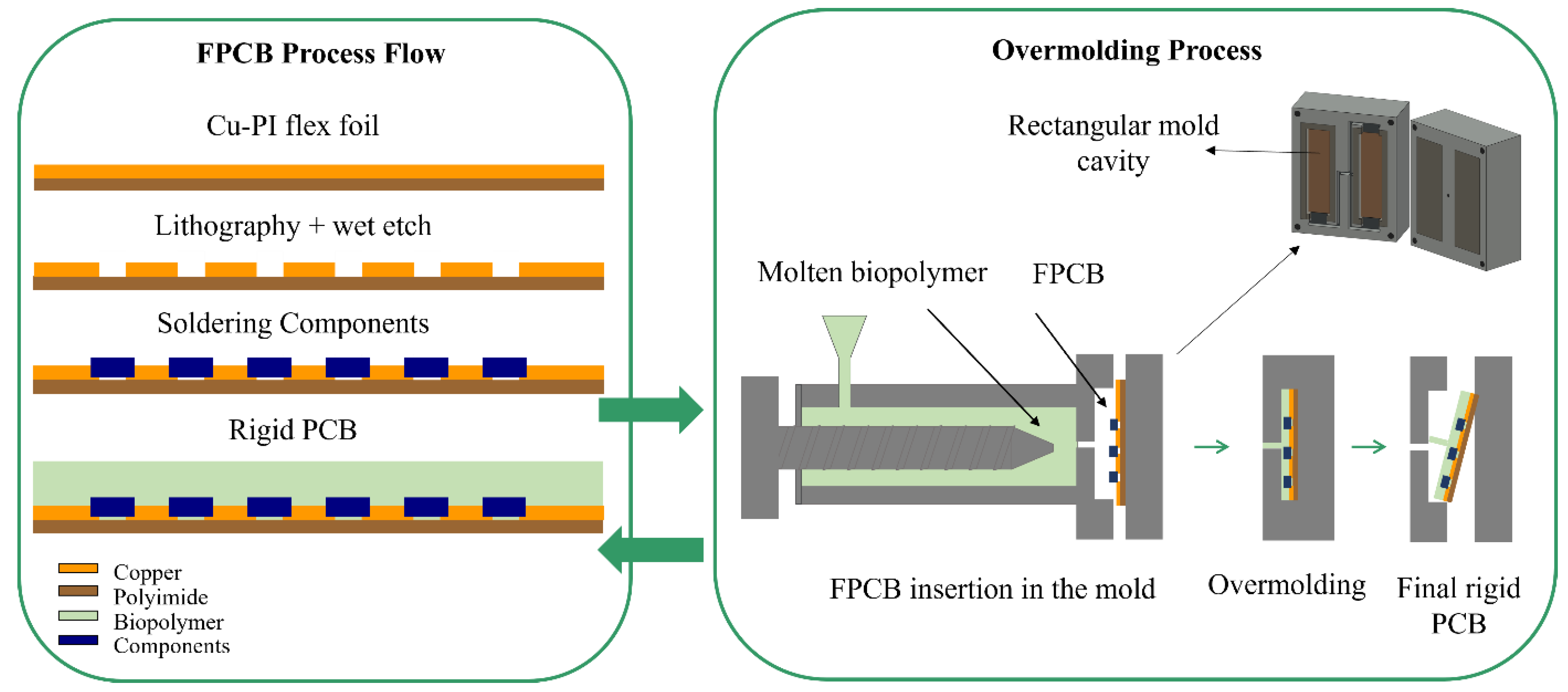
The process steps are divided into four main sections: FPCB (flexible PCB) design and fabrication, the overmolding of the biopolymers, adhesion optimization, and end-of-life practices.
3.1. FPCB Design and Fabrication
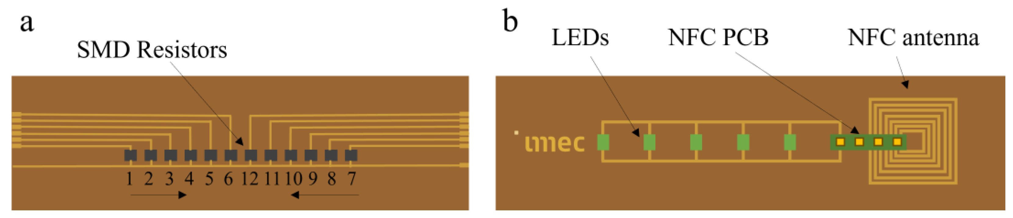
The first circuit design shown in
Figure 1a consists of two groups of 12 SMD resistors (0 Ω resistors) placed in parallel and linked over long Cu tracks to pads that are positioned left and right. Cu connection pads are patterned on the PI in a way that facilitates the measurements of resistance values.
As another circuit, a demonstrator was selected to power LEDs wirelessly using an integrated NFC antenna avoiding the need for an integrated battery. Doing so, the circuit functionality can be evaluated without connecting probes to the conductive traces. The circuit is therefore not exposed to the clamping force of the injection molding machine. The circuit design is shown in
Figure 1b.
As mentioned, three commercial flexible foils are used as the substrate for patterning the copper traces. PI has a high thermal resistance, outstanding mechanical and chemical properties, and stable dielectric properties over high temperatures (up to 400 °C), which makes it a widely used substrate in FPCB industry. The FPCB was fabricated in-house through PCB manufacturing technology. The process flow includes patterning the copper structure by lithography and wet etching. Afterwards, the solder paste (lead-free SAC305) is manually applied to the soldering pads using a dispenser followed by the mounting of the components on the defined areas. Finally, the solder paste is reflowed by vapor phase soldering (VPS) at 230 °C (vapor phase reflow oven IBL SLC 300).
3.2. Rigid PCB Production Using Overmolding Technology
Overmolding generally refers to applying a material over another material or object using injection molding technology. To achieve the desired part quality, dimensional accuracy, and production efficiency, injection molding parameters must be optimized for biopolymers (PLA and PHB). Both biopolymers are hygroscopic; therefore, the biopolymer pellets were dried for 24 h at 60 °C in a FarrgTech dryer (Austria) before overmolding to avoid the presence of moisture and to prevent the generation of bubbles and air traps during the overmolding process.
An Engel 80T injection molding machine (Austria) is used to overmold the FPCB. As schematically shown in
Figure 2, it is performed by inserting the FPCB into the mold cavity. The mold is closed on the foil and the injection screw pushes the molten biopolymer towards the mold cavity. The molten biopolymer flows and starts covering the FPCB. Following that, the biopolymer solidifies rapidly, and the mold opens again and ejects the part out from the machine.
Figure 2 demonstrates the two main fabrication methods of FPCB and overmolding.
In this study, a rectangular aluminum mold with a dimension of 150 × 40 × 1.5 mm3 was used. One of the molds has one flow entry and the other one has two flow entries. The double-entry mold resulted in some air traps and shrinkage in the middle of the samples which is not desirable. Therefore, the single-entry mold was selected for this research.
During the injection molding process of polymers, various defects may arise if the process parameters are not properly adjusted. Some of the most common defects include warpage (bending due to uneven shrinkage), flash (excess material leaking from the mold cavity), short shots (incomplete mold filling), and bubbles (trapped air within the material). These defects can affect the structural integrity, functionality, and appearance of the final product [
30].
To achieve a high dimensional accuracy and optimal part quality, it is crucial to optimize the injection molding parameters for each biopolymer. The key parameters affecting the final quality include material temperature, mold temperature, injection speed, cooling time, and holding time. Holding time refers to the duration of which pressure is applied to the molten material after the mold cavity is filled but before cooling begins. It ensures that material shrinkage is compensated, preventing voids and incomplete packing [
30].
3.3. Adhesion Optimization
The adhesion between the PI foil and the PLA/PHB substrate is a crucial factor influencing the mechanical stability and reliability of the PCB. PI and the two selected biopolymers (PLA and PHB) show a very poor adhesion towards the three types of PI foils after overmolding. Therefore, two adhesion improvement methods were evaluated, and their effectiveness was investigated. Oxygen plasma surface treatment has been performed to activate the PI foil surface prior to overmolding. In addition to that, a thermoplastic polyurethane (TPU) tie layer was used as an adhesive to improve the bonding.
For these types of circuitry, the majority area of the flex circuit (Cu side) consists of exposed PI, resulting from the etching of the covering Cu layer. Hence, for the adhesion evaluation experiments, the surface treatment was conducted on completely etched PI foils. Note that for the Pyralux and Shengyi foils, the outer layers consist of adhesive layers (acrylic and epoxy based, respectively).
The oxygen plasma treatment was performed with a PICO—Diener electronic GmbH & Co. KG, Germany. The power and frequency were adjusted to 190 W and 40 kHz, respectively. The samples were treated for 2 min with an oxygen pressure of 0.8 mbar.
For the other improvement method, a TPU tie layer is applied on the etched PI foil using a vacuum lamination method (Lauffer RLKV 25) at a 120 °C temperature and 20 N/cm2 pressure for 30 min. Afterwards, the TPU-laminated foil is overmolded by biopolymers.
To compare the effectiveness of each method, the adhesive strength is measured using the 180-degree peel test method. To measure the peel strength, an Instron 5543 universal testing machine equipped with a 500 N load cell is used. The bilayer samples were cut to a 3 cm width and fixed to the grips to measure the force (
Figure 3). Three identical samples of each case were evaluated to ensure reproducibility.
3.4. End-of-Life Practices
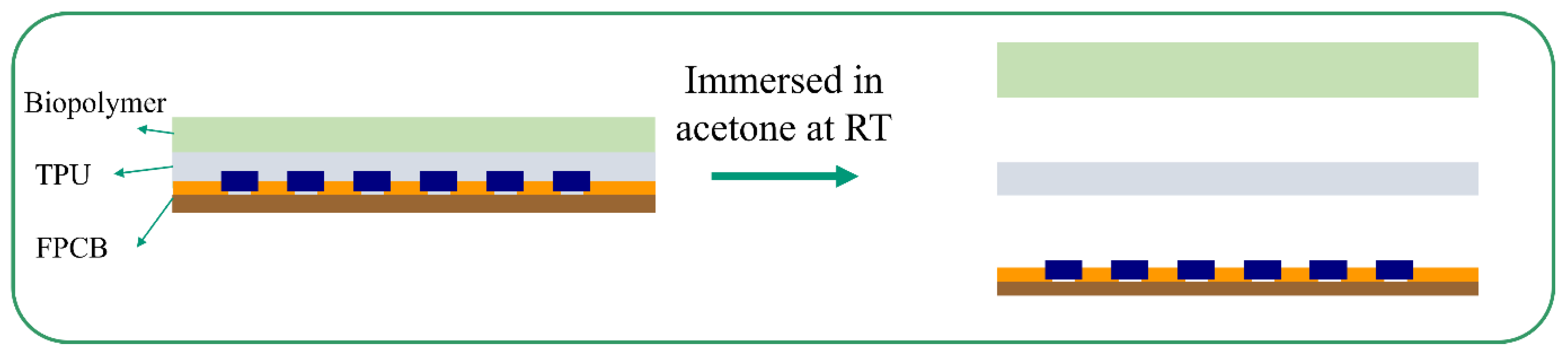
In this study, as the end-of-life treatment, we analyzed debonding and composting methods separately. The rigid PCBs including the TPU layer are selected as a sample test in this section.
3.4.1. Debonding Strategy
The debonding approach suggests a separation of the biopolymer part from the FPCB part using a liquid. This allows the electrical components to be potentially reused or recycled.
The rigid PCBs consist of a PI foil with copper tracks and components, a laminated TPU tie layer, and an overmolded biopolymer. To separate the layers, the samples are immersed in an acetone solution and monitored over time. The debonding concept is demonstrated in
Figure 4.
The samples were cut into sizes of 4 × 2.5 cm2 and immersed in the analytical acetone solution (p. 99+% from Chemlab, Belgium) in a jar at room temperature.
3.4.2. Composting
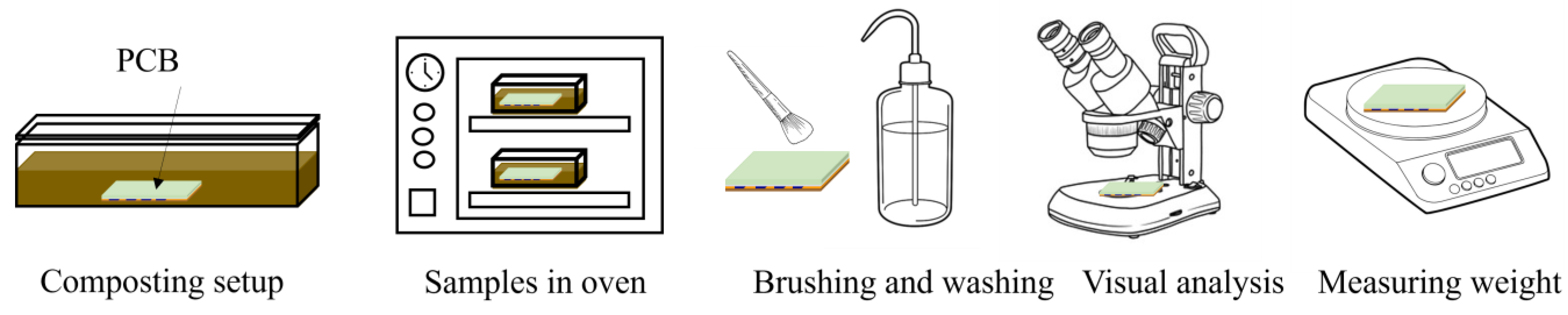
On the other hand, a quantitative composting method is used to decompose the biopolymer part through microorganism digesting the nutrients of the biopolymers. Afterwards, the copper tracks and components are recovered from the compost.
Four small glass containers were filled with organic composting soil. The samples were cut into 4 × 2.5 cm
2 and buried within the compost. Four samples consisting of one pure PLA, one PCB with PLA, one pure PHB, and one PCB with PHB were selected. The pure biopolymers are considered as a reference. At the start of the experiment, the samples were visually inspected and weighed in a dry condition. Next, the containers were put in an oven at 58 ± 2 °C for 60 days. The medium was kept moist by adding deionized water every day and the soil was gently moved for better oxygen exchange. For checking the degradation behavior, the samples were removed from the compost, and brushed and washed gently with water to remove soil debris followed by drying at 40 °C for 5 h in the oven. Afterwards, the samples were visually analyzed for any color or morphological changes and then reweighed (
Figure 5). The analyses were performed every 15 days.
The weight loss was calculated with the following Formula (1):
where
is the initial weight of the samples, and
is the weight of the samples after they are removed from the compost at different time points.
4. Results and Discussion
4.1. Overmolding Process Parameters Optimization
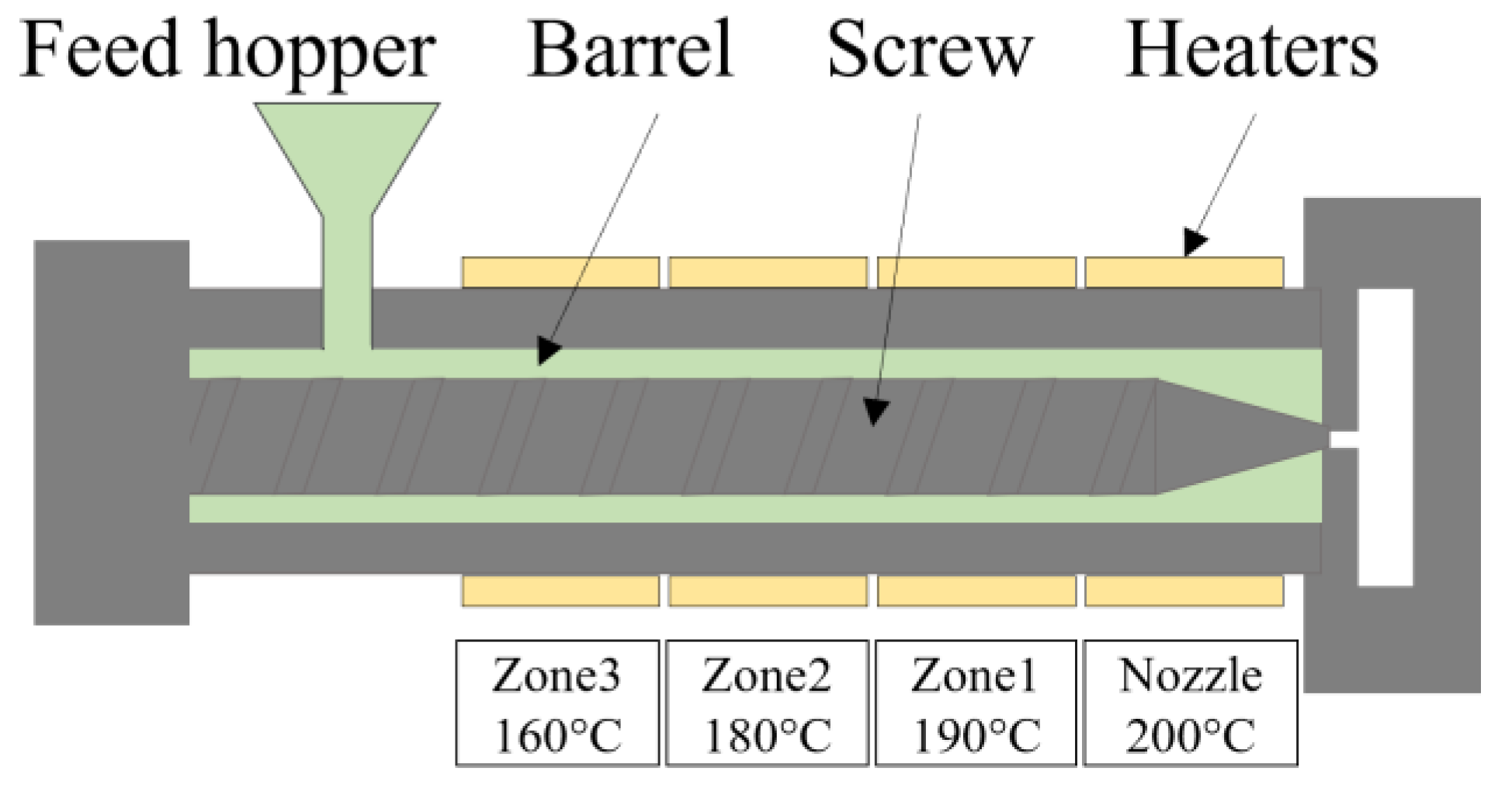
Process optimization was initially conducted without inserting the flexible foil to fine-tune the injection molding parameters. The barrel temperature of the injection molding machine was set within the range recommended by the manufacturer and remained constant throughout the process, as illustrated in
Figure 6. The nozzle temperature is crucial because it ensures that the polymer is fully melted before it is injected into the mold under applied pressure.
The optimization process began with PLA. The mold temperature, injection speed, and cooling time are maintained constant at 30 °C, 120 mm/s, and 45 s, respectively. The two main variables adjusted to optimize the molding process were the dosing length and switchover point, which directly affect the amount of material injected into the mold and the transition between the filling and packing phases.
The dosing length refers to the amount of molten plastic (shot size) that is prepared in the barrel before each injection cycle. The screw retracts by a set distance to accumulate the correct volume of molten material. The switchover point defines the position at which the injection phase switches from velocity-controlled filling to pressure-controlled packing. It is crucial to prevent defects such as flashing or short shots.
In the first cycle, the dosing length was set to 30 mm, and the switchover point was 5 mm, meaning that the screw initially retracts 30 mm to accumulate molten material, but moves forward 25 mm to inject it into the mold cavity. With these settings, excess material overflowed from the mold (flash and burr defects), indicating that too much material was injected.
To counteract this, the switchover point was increased to 15 mm, meaning the transition from filling to packing happens earlier. However, this adjustment led to an underfilled mold (short shot), because the material did not flow sufficiently due to its high viscosity.
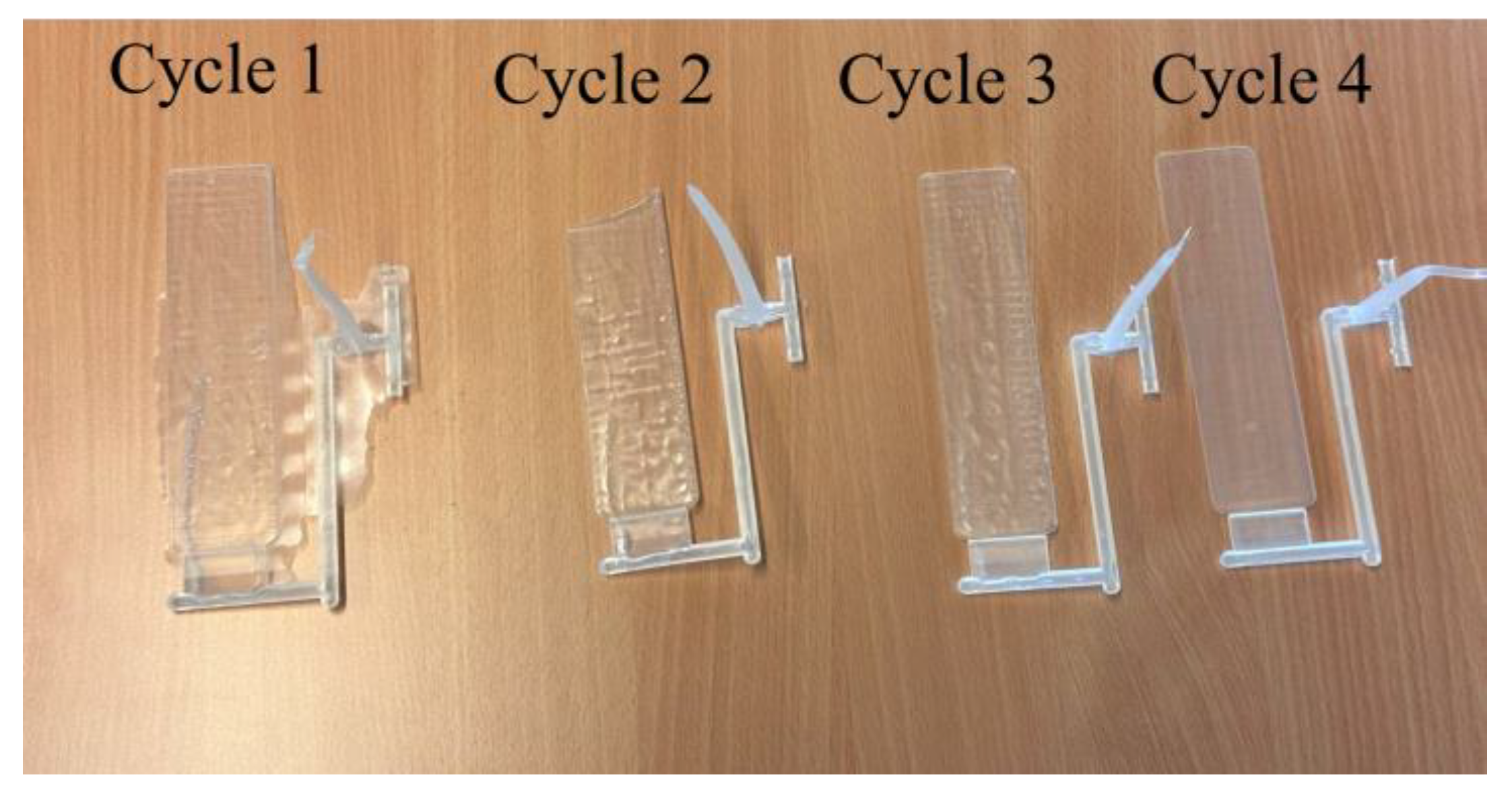
Thus, the switchover point was adjusted to 12 mm allowing the mold to be completely filled. However, shrinkage and an uneven surface finish were observed. To address this issue, the holding time was increased to 2 s, ensuring that the material had sufficient time to settle and solidify properly, resulting in a smooth and well-defined final shape.
Table 2 (
Figure 7) summarizes the optimization cycles performed for PLA molding.
The same parameters were applied to the PHB. The switchover point was initially set at 12 mm, and the holding time was set at 2 s. This setting resulted in some burrs and flashes. In the second stage, the switchover point was changed to 14 mm and the holding time was decreased to 0 s. The mold was not filled, resulting in a short shot. Therefore, the holding time was increased to 2 s, and the switchover point to 14 mm. The desired part was achieved in cycle 3 as shown in
Table 3 (
Figure 8).
Five tests confirmed the repeatability of these parameters, resulting in identical molded pieces. Optimized parameters were tested with PI foil inserted into the mold, and no defects were found.
4.2. The Validation of Circuit Functionality
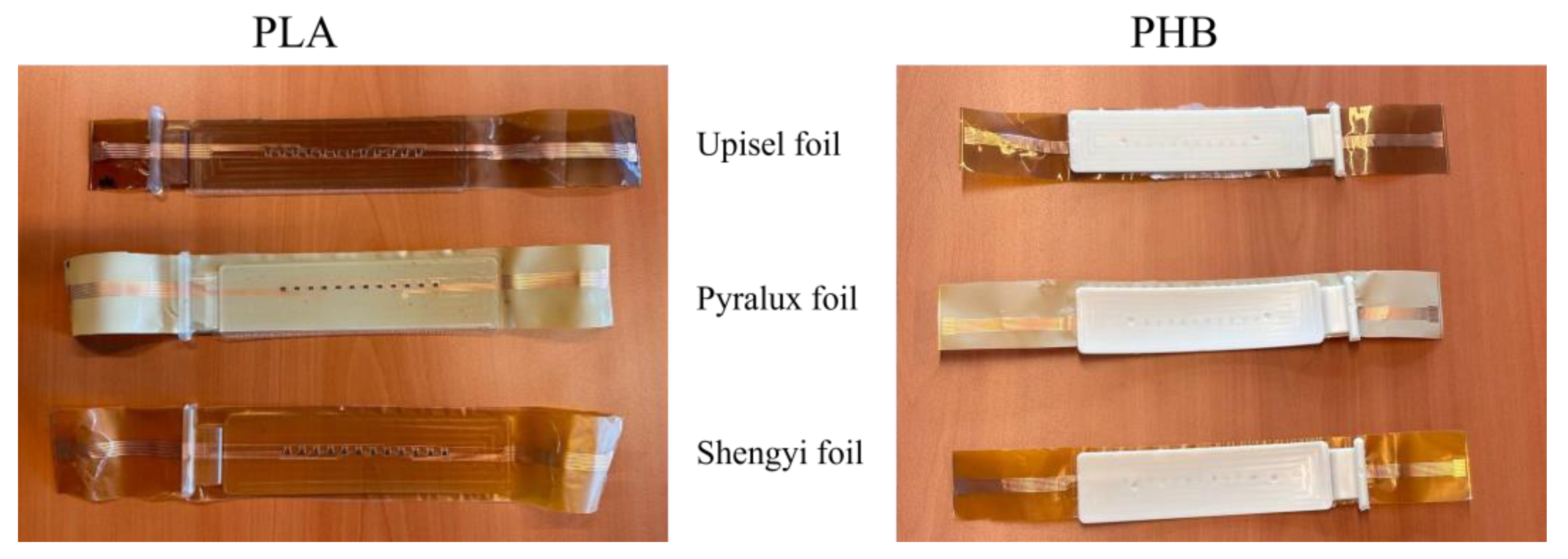
The resistor circuits on three different PI foils after overmolding are demonstrated in
Figure 9. They were all functional with a slight increment in the resistance value after overmolding.
A component’s measured resistance is the sum of its resistance, the Cu trace’s resistance, the soldered connection’s resistance, and the probe’s contact resistance:
The
of the component is the value before assembling the resistors on the foil. Each mounted 0 Ω resistor has a different track length (
L) between the component and the connection pad. This length has an effect on the final value according to resistance formula (
) with R being the resistance,
being the resistivity,
being the length, and
being the cross-sectional area) showing a direct relation to its length
L [
31].
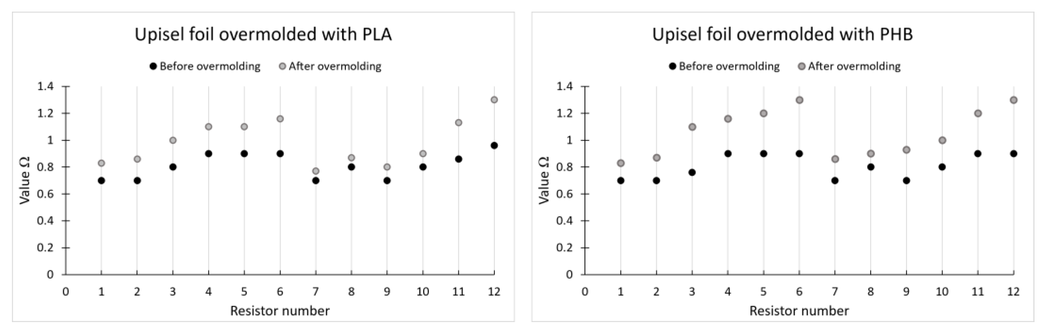
Figure 10 presents average
values for Upisel foil before and after overmolding with PLA and PHB.
Overmolding slightly increased the measured resistance. This change could be attributed to the oxidation of Cu tracks because of heat, the contact resistance of the probe, or the local reduction in Cu track thickness due to mold clamping pressure [
31].
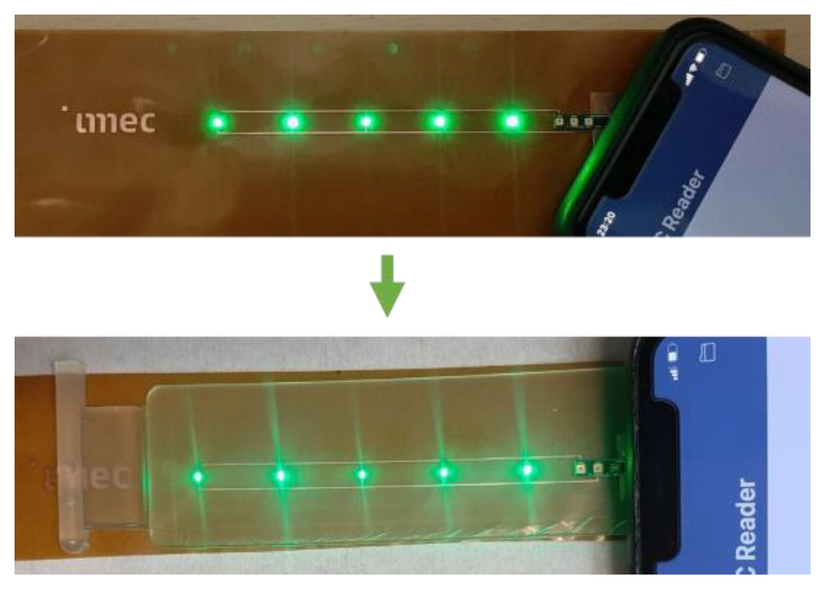
Regarding the demonstrator circuit, a smart phone with an NFC reader application was used to power the LEDs wirelessly. By keeping the smart phone close to the NFC antenna, the voltage from the phone battery is induced to the antenna and transferred to the LEDs through an NFC chip.
Figure 11 shows the functionality of the LEDs after the overmolding process.
Functionality measurements of the fabricated test circuits demonstrated that the signal connection was maintained after overmolding with PLA and PHB.
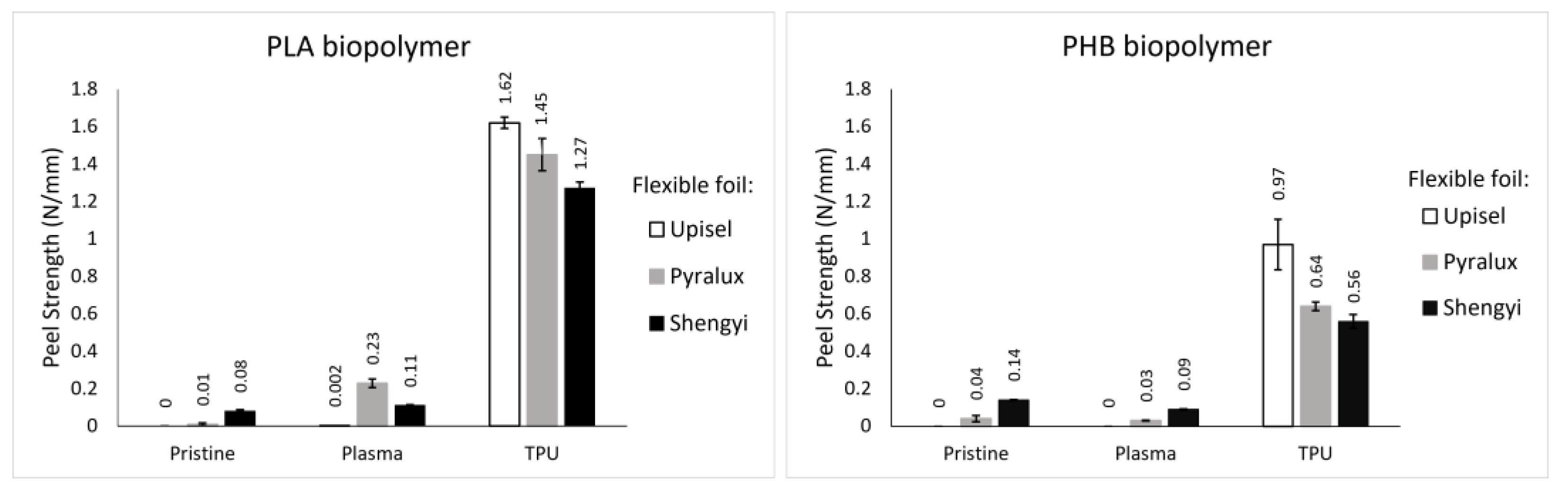
4.3. Adhesive Strength Measurement
The peel test results of adhesion between the biopolymer (PLA or PHB) and three flexible foils in different conditions of a pristine (no-treatment), oxygen plasma, and TPU layer are shown in
Figure 12.
As can be seen in the bar chart, the pristine Upisel foil shows no adhesion and peels off spontaneously from both biopolymers upon ejection from the mold. However, the adhesive strength related to the Pyralux and Shengyi samples were measurable but negligible (less than 0.1 N/mm). This could be attributed to the existence of adhesive layers (acrylic or epoxy) on the mentioned foils.
After treating the foils with oxygen plasma, oxygen functional groups such as hydroxyl (-OH) and carbonyl (C=O) groups are introduced to the foil surfaces. These polar functional groups can potentially improve the adhesion to overmolded PLA.
Using a TPU layer between PI foils and biopolymers resulted in significantly higher peel strengths. It was expected because this TPU has excellent adhesive properties to a large variety of polymer foils.
The approach of using the TPU layer shows a strong bond between the FPCB and biopolymer and guarantees the long-term durability of the rigid PCB. To ensure environmental sustainability, it would be appropriate to use biobased or biodegradable TPU, which is currently in the development phase [
32].
4.4. End-of-Life
4.4.1. Debonding
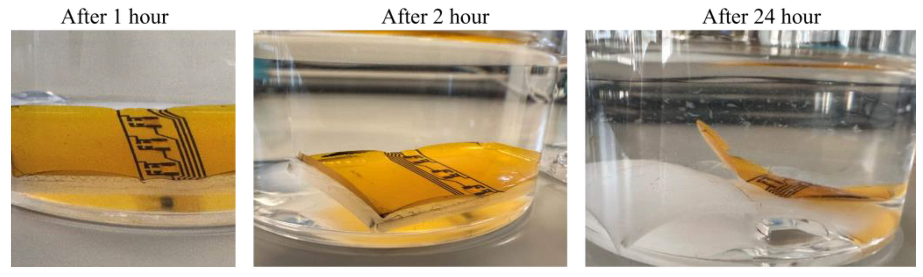
The debonded layers after being recovered from the acetone solution are shown in
Figure 13. As can be seen, the three fractions of the FPCB, TPU, and biopolymer are detached.
For all the samples, the TPU started to wrinkle after about 1 h. After 2 h, the PI foil and biopolymer showed a small delamination from each other. After 24 h, the three parts were completely delaminated, and the fractions were recovered.
Figure 14 illustrates the debonding phenomenon over time.
This method allowed for the complete separation of the FPCB, TPU, and biopolymer under mild chemical treatment, without using additional mechanical and thermal processes. It is possible to use an ultrasonic bath or raise the temperature to enhance the separation rate; however, we explored the possibility of debonding with having the least environmental effects compared to other solvents. Alternative solvents can be used such as dimethyl formamide (DMF) and tetrahydrofuran (THF) for dissolving TPU; however, these chemicals bring more environmental and health hazards compared to acetone [
33].
The electrical components and copper tracks remained intact (
Figure 13) and retained their electrical properties. The debonded layers of biopolymers present a valuable opportunity for upcycling, where they can be repurposed into new products with an enhanced quality and value for different applications, such as advanced composites, and biodegradable packaging [
34]. The debonding method could be an energy and time-saving approach by avoiding the production of virgin biopolymer.
4.4.2. Quantitative Composting Analysis
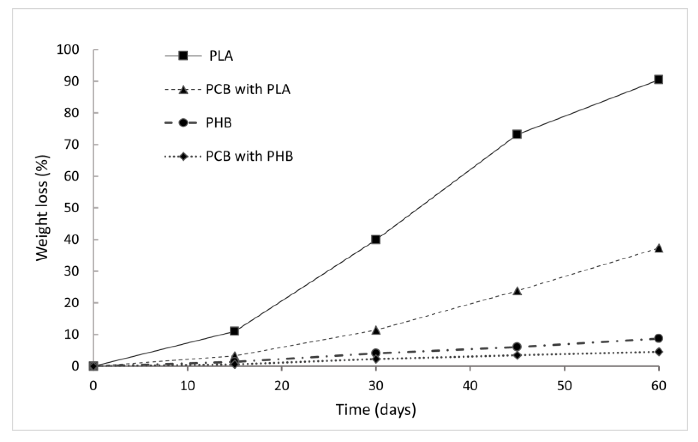
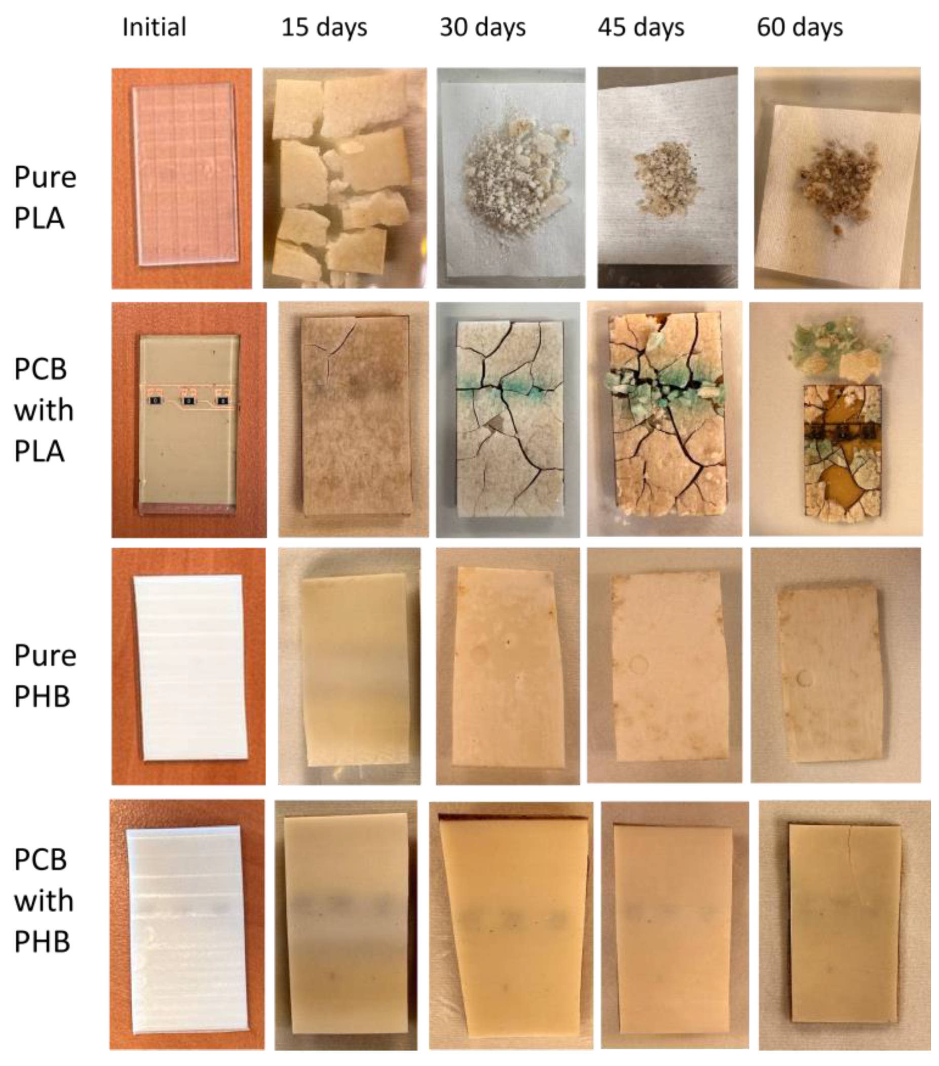
The weight change after 60 days of storage in the composting setup is represented in
Figure 15. The weight loss shows a consistent trend over time. The pure PLA was degraded by more than 90% after 60 days, confirming biodegradability. However, the PCB with PLA showed a 37.3% weight loss after 60 days. It should be noted that metals could have negative impacts on the compost quality. PHB samples did not show any significant weight loss.
In samples with circuits, the degradation happened at the biopolymer side and no degradation was observed on the PI side. The biodegradation process of the four samples is shown in
Figure 16. As can be seen, the pure PLA disintegrated into coarse parts after 15 days of storage in compost. PCB with PLA also showed some holes and surface change during the first 15 days. The PLA samples exhibited a significant color change during the composting. The amorphous regions of the polymers degrade faster than the crystalline regions. This selective degradation leads to an increase in the degree of crystallinity and opacity [
35]. In addition, hydrolysis and oxidation reactions during biodegradation could result in the formation of shorter polymer chains. These chemical changes can alter the optical properties of PLA, resulting in color changes (e.g., yellowing or darkening) [
36]. The blue-green patina color in the PCB sample is the result of the reaction of copper with oxygen and moisture [
37].
In the case of PHB samples, a slight deterioration showed up with minor holes after 30 days. The PCB with PHB almost maintained the same appearance as the initial sample. According to research [
38], the degree of humidity plays a key role in the degradation of PHB. Moreover, PHB has a crystalline structure which makes it resistant to microbial attack since their tightly packed molecular structure hinders the penetration of enzymes. PHB degradation is also dependent on thermophilic microbes that produce PHB-depolymerase enzymes [
39]. Therefore, the degradation process may be delayed if these microbes are absent or present in low concentrations in our compost media.
As a conclusion, PLA shows a faster degradation due to its higher amorphous fraction after molding compared to PHB. PCB samples exhibit a slower weight loss due to their smaller surface area exposed to microorganisms. It should be noted that the proposed PCBs showed no sign of natural degradation during the usage phase.
4.4.3. End-of-Life Strategies and Sustainability
The end-of-life phase is a critical aspect of evaluating the environmental sustainability of PCBs. In
Section 4.4.1., a debonding strategy is discussed using a mild solvent treatment (acetone), enabling the separation of the biopolymer from the PI and copper layer without mechanical grinding or high-temperature processes. This separation method facilitates material recovery and recycling, while preserving the electrical and mechanical properties of the PI-copper layer for potential reuse [
40].
Among biopolymers, industrial composting is a widely recognized end-of-life strategy. Under controlled conditions (temperature ≥58 °C, regulated humidity, and microbial activity), both PLA and PHB can be biodegraded into CO
2, water, and biomass offering a low-energy, low-impact alternative to landfill or incineration. However, improper disposal in uncontrolled environments (e.g., home composting) may result in an incomplete degradation and the formation of microplastics [
41].
In addition, mechanical recycling is feasible for PLA and PHB-based PCBs. This method involves shredding the PCB and separating metallic and non-metallic parts. However, repeated processing can lead to a reducing of the mechanical and thermal performance of the biopolymer. Chemical recycling, including hydrolysis, or enzymatic depolymerization, enables the recovery of high-purity monomers like lactic acid or 3-hydroxybutyric acid. These processes allow closed-loop recycling and retain material quality. However, they require solvents, catalysts, and energy input, making them less favorable in terms of environmental cost [
42,
43].
Each end-of-life strategy has trade-offs. The possibility of material recovery through a debonding process as shown above, biodegradation under industrial composting, or chemical depolymerization gives biopolymer-based PCBs a more favorable environmental profile than conventional alternatives [
44].
4.5. Life Cycle Assessment Perspective
From a life cycle assessment (LCA) perspective, the environmental impact of PLA and PHB substrates is significantly lower compared to FR4. In general, the production of FR4 involves high greenhouse gas emissions, energy-intensive manufacturing processes, and extensive resource extraction. In contrast, PLA and PHB production typically emit fewer greenhouse gases due to their bio-based origin.
A benchmarking analysis conducted by NatureWorks assessed the environmental impact of Ingeo PLA compared to traditional petroleum-based polymers such as polyethylene terephthalate (PET) and polystyrene (PS). The study reports that the cradle-to-gate nonrenewable energy use for PLA is approximately 42 MJ/kg, whereas petroleum-based polymers typically require 60–100 MJ/kg, depending on the energy source used. In terms of greenhouse gas (GHG) emissions, PLA emits approximately 1.3–1.5 kg CO
2-eq per kg, while PET and PS emissions range between 3.0–6.0 kg CO
2-eq per kg. The lower emissions of PLA are attributed to its bio-based origin, which makes it a more sustainable alternative [
45].
Similarly, Naji et al. analyzed the cradle-to-gate LCA of PLA-based composite and FR4 PCBs, demonstrating that PLA-based substrate has a Global Warming Potential (GWP) of 0.63 kg CO
2-eq, whereas FR4 has a significantly higher GWP of 6.29 kg CO
2-eq due to high emissions during epoxy and fiber glass production. Additionally, FR4 exhibits a substantially higher Human Toxic Potential (HTP) of 19.5 kg DCB-eq, compared to 2.32 kg DCB-eq for PLA-based substrates. Since PLA is biodegradable under industrial composting conditions, its organic fraction decomposes into water, CO
2, and biomass, thereby minimizing waste accumulation [
24].
A literature review by Fonseca et al. compared the environmental impacts of PLA with fossil-based plastics, such as polypropylene (PP), PET, and PS. Their study highlights that PLA has lower impacts in fossil fuel depletion and ozone layer depletion, but higher eutrophication and human toxicity impacts due to the use of fertilizers in agricultural feedstock production. However, utilizing agricultural byproducts (e.g., sugarcane bagasse) instead of food crops can significantly reduce the environmental toxicity of PLA production. One of the primary challenges of biopolymer production is its competition with food supply chains, necessitating the development of alternative biomass sources, such as agricultural residues or waste-derived feedstocks [
46].
Regarding PHB production, Rostkowski et al. analyzed its life cycle impacts, comparing biogas-based PHB production with plant-derived PHB. Their study found that the total energy requirement for PHB production from waste biogas is 37.4 MJ/kg, whereas corn-based PHB production requires 41.9 MJ/kg. This suggests that biogas-derived PHB is more sustainable, as it requires less energy, water, and land, unlike corn-based PHB. This demands significant agricultural input. Despite this, PHB production remains less energy-intensive than petroleum-based polymers [
47].
The sustainability benefits of our approach are primarily due to the reduced carbon footprint and energy consumption of biobased and biodegradable polymers, as well as the improved end-of-life options for PCBs. In our approach, we utilize PLA/PHB (1.5 mm) as the main substrate, but we also use a 50 µm PI layer and a 100 µm TPU layer to enhance performance and durability. While the addition of PI and TPU introduces some environmental impact, their contribution remains minimal compared to the significant reduction in CO2 emissions, energy consumption, and material weight achieved by replacing FR4 with PLA/PHB. Furthermore, our approach facilitates the easier material separation and potential compostability of PLA/PHB, providing a more sustainable end-of-life solution compared to FR4, which typically ends up in landfills or requires high-energy recycling processes.
Comparing the weight of our PLA-based PCB with FR4 PCB provides a better insight into the lower environmental impacts of the proposed approach. The total weight is calculated using following Equation (3):
The PLA-based thickness will be 1.65 mm considering PI and TPU layers. The densities of each layer are .24 g/cm3, = 1.42 g/cm3, and = 1.2 g/cm3. The total weight for the dimension of 150 × 40 × 1.65 mm3 results in 12.31 g. For a 150 × 40 × 1.6 mm3 FR4-based PCB, the total weight is approximately 17.76 g. This shows in a 30.71% reduction in material weight. This lower mass contributes to resource savings and a reduced environmental impact.
According to Naji et al. data [
24], we can estimate the GWP of the calculated weight of PCBs. Our PLA-based PCB results in a CO
2 footprint of approximately 0.00703 kg CO
2-eq (only PLA is considered), while an equivalent FR4 PCB substrate emits about 0.111 kg CO
2-eq, representing a 93.72% reduction in greenhouse gas emissions.
It should be noted that PI and TPU will increase the total CO2 emission for PLA-based; however, in view of their low thickness, the total value is expected to remain lower than conventional FR4. Thus, while the PI and TPU layers introduce a minor environmental impact, it is more than compensated by using biopolymers. This demonstrates that biopolymer-based PCBs can serve as an eco-friendly alternative in electronic applications.


 ,
, 


