Article

Voltage Balancing of a Bipolar DC Microgrid with Unbalanced Unipolar Loads and Sources

by
Mateus Pinheiro Dias
1,*,
Debora P. Damasceno
1,
Eliabe Duarte Queiroz
1,
Kristian P. dos Santos
2,
Jose C. U. Penã
1 and
José A. Pomilio
1
1
Departamento de Sistemas e Energia (DSE), Universidade Estadual de Campinas, Campinas 13083-852, Brazil
2
Departamento de Eletrotécnica, Federal Institute of Education, Science and Technology of Piauí, Parnaíba 64211-145, Brazil
*
Author to whom correspondence should be addressed.
Processes 2025, 13(11), 3734; https://doi.org/10.3390/pr13113734
Submission received: 29 September 2025 / Revised: 7 November 2025 / Accepted: 14 November 2025 / Published: 19 November 2025
(This article belongs to the Special Issue Advances in Power Converters in Energy and Microgrid Systems)

Abstract

This paper presents the validation of a voltage balancing converter for a bipolar DC microgrid designed to ensure reliable operation in both grid-connected and islanded modes. This microgrid includes unipolar constant power loads (CPL), a unipolar Battery Energy Storage System (BESS), and local PV generation. The BESS converter employs a V–I droop strategy using only inductor current feedback, reducing sensing requirements while maintaining plug-and-play capability and ensuring smooth transitions between connected and islanded modes. In such a microgrid, the voltage balancing converter regulates the differential voltages under severe unbalanced load conditions and during transients caused by changes in unipolar loads and sources. The experimental results validate the voltage balancing strategy across various scenarios in a small-scale prototype. The results show tight voltage regulation under unbalanced conditions, and smooth transitions during load transients and unintentional islanding, even if there is no dc voltage source in one of the poles of the bipolar dc bus. For both conditions, the imbalance between the unipolar voltages is less than 0.5% of the total bipolar voltage.

1. Introduction

The global electricity demand is projected to exhibit the fastest growth rate during the triennium of 2025–2027. This increase is primarily driven by industrial expansion, increased air-conditioning usage, ongoing electrification, the large-scale integration of electric vehicles (EVs) into modern power systems, and the worldwide proliferation of data centers. The annual growth rate is expected to reach approximately 4 % until 2027, corresponding to 3500 TWh [1]. By 2027, solar photovoltaic (PV) systems are expected to contribute nearly 50 % to global electricity demand [1].
In 2024, Brazil’s electricity demand increased by 6 % [1]. According to the national energy balance, hydropower remains the dominant source in the country’s electricity mix. Renewable sources account for 89 % of the domestic electricity supply, with the residential sector representing 27.5 % of the final consumption [2].
The penetration of renewable energy sources, including PV, wind energy conversion systems, and hydropower, has expanded substantially in recent years [3,4]. Such expansion of distributed generation poses significant challenges to the conventional centralized grid paradigm.
The incorporation of photovoltaic technology into buildings is generally termed building-integrated photovoltaic (BIPV) systems [5,6]. A cost-effective BIPV solution was proposed [7], employing a high step-up PV dc-building module combined with an inverter.
A power distribution system (PEDF) comprising three main components—PV generation, energy storage, and dc distribution—was presented in [8]. Similarly, in [9], two 2.1 kWp PV systems, operating within a 190–370 V range, supplied power to a 48 V LED lighting dc bus at the CleanTech-One Level Five laboratory.
Moreover, an IoT-based multifunctional system was deployed in a 1.5 kW PV dc residential building in Tamil Nadu, India [10]. The proposed strategy reduced total losses by 18 % through load prioritization and demand-side management. Furthermore, the integration of IoT into building automation improved energy management and enhanced occupant comfort [11].
DC microgrids are generally organized into two configurations: unipolar and bipolar bus structures. The unipolar topology comprises positive and negative poles, while the bipolar topology includes three poles: positive, negative, and a central neutral point.
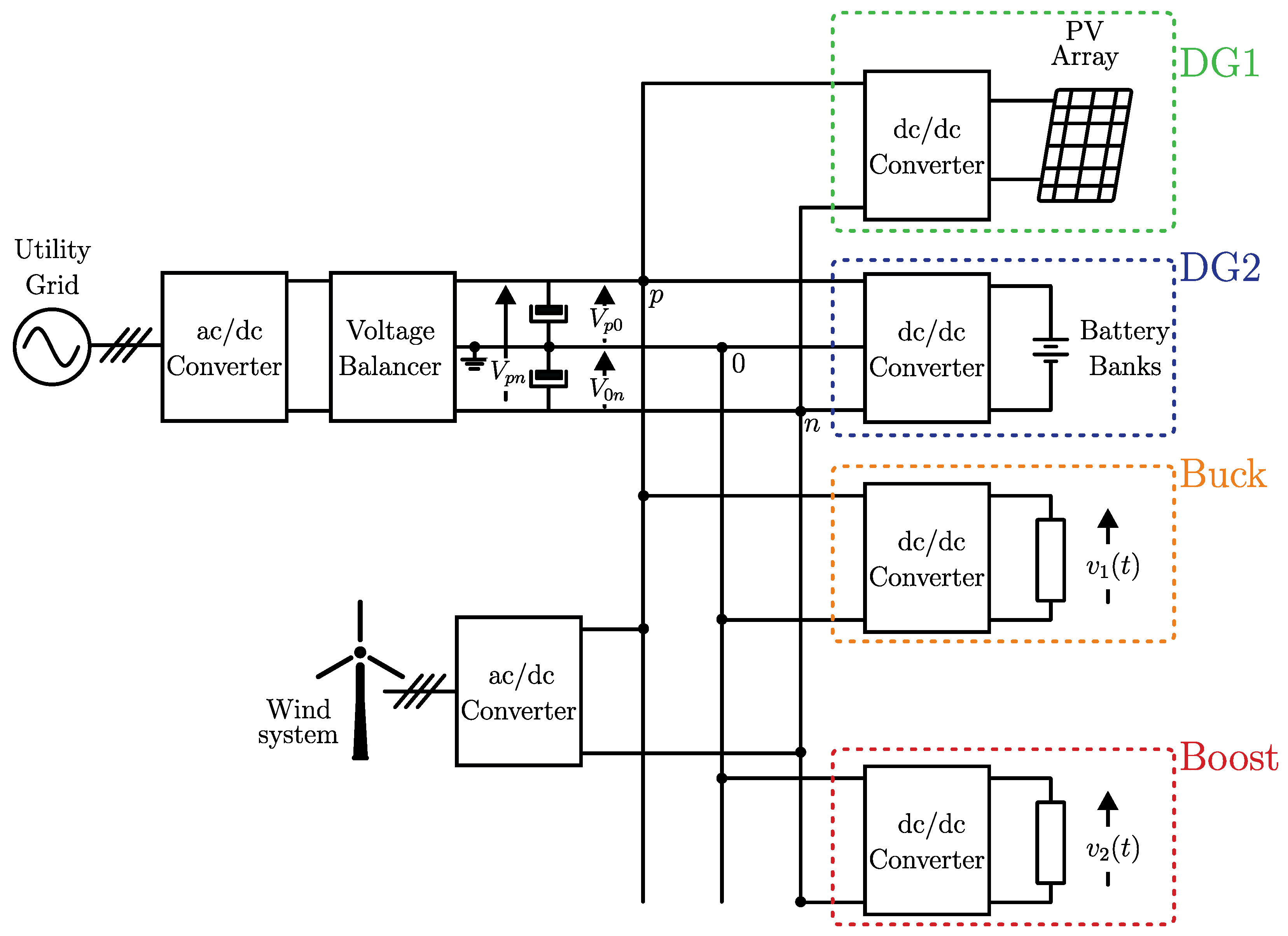
Figure 1 illustrates a bipolar dc microgrid based on a p–0–n bus structure, which integrates several distributed generators (DGs), such as an energy storage system (ESS), a wind energy conversion system (WECS), a PV array with an embedded dc–dc converter, and electronic dc loads such as buck and boost converters.
In a bipolar dc microgrid, the presence of three electrical poles allows renewable energy sources and dc loads to be connected either between the positive pole and the neutral point (p–0), between the neutral point and the negative pole (0–n), or directly between the positive and negative poles (pn).
Several pilot projects have already implemented bipolar dc microgrids. For example, a hybrid ac-dc distribution system with a ± 750 V dc bipolar grid and a 380 V dc bus has been deployed in Finland [12].
A representative medium- and low-voltage dc distribution system has been deployed by State Grid Jiangsu Electric Power in Wujiang, China. The installation comprises three bipolar dc levels, namely ± 10 kV , ± 375 V , and ± 48 V . This infrastructure supplies a wide assortment of dc-based applications, including industrial facilities, data centers, residential consumers, and rooftop photovoltaic units located in the Hongyi area [13].
A key advantage of the bipolar configuration is the flexibility of voltage-level operation [14]. The reliability of the system is improved because operation can continue with a single pole in the event of a pole fault. In such cases, either the p–0 or 0–n bus ensures continuous supply to dc loads, thereby improving the power transmission capability [14,15].
Although dc microgrids offer numerous advantages, they still face two major challenges: lack of standardization and unresolved protection issues [16]. Furthermore, grounding methods, voltage level definitions, and islanding detection techniques are still under investigation [17,18,19].
A voltage balancer is employed to maintain the balance between v p 0 and v 0 n even in the presence of unbalanced load conditions. Furthermore, it prevents dc current injection when the ac–dc converter is interfaced with a three-phase four-wire system [20,21,22,23].
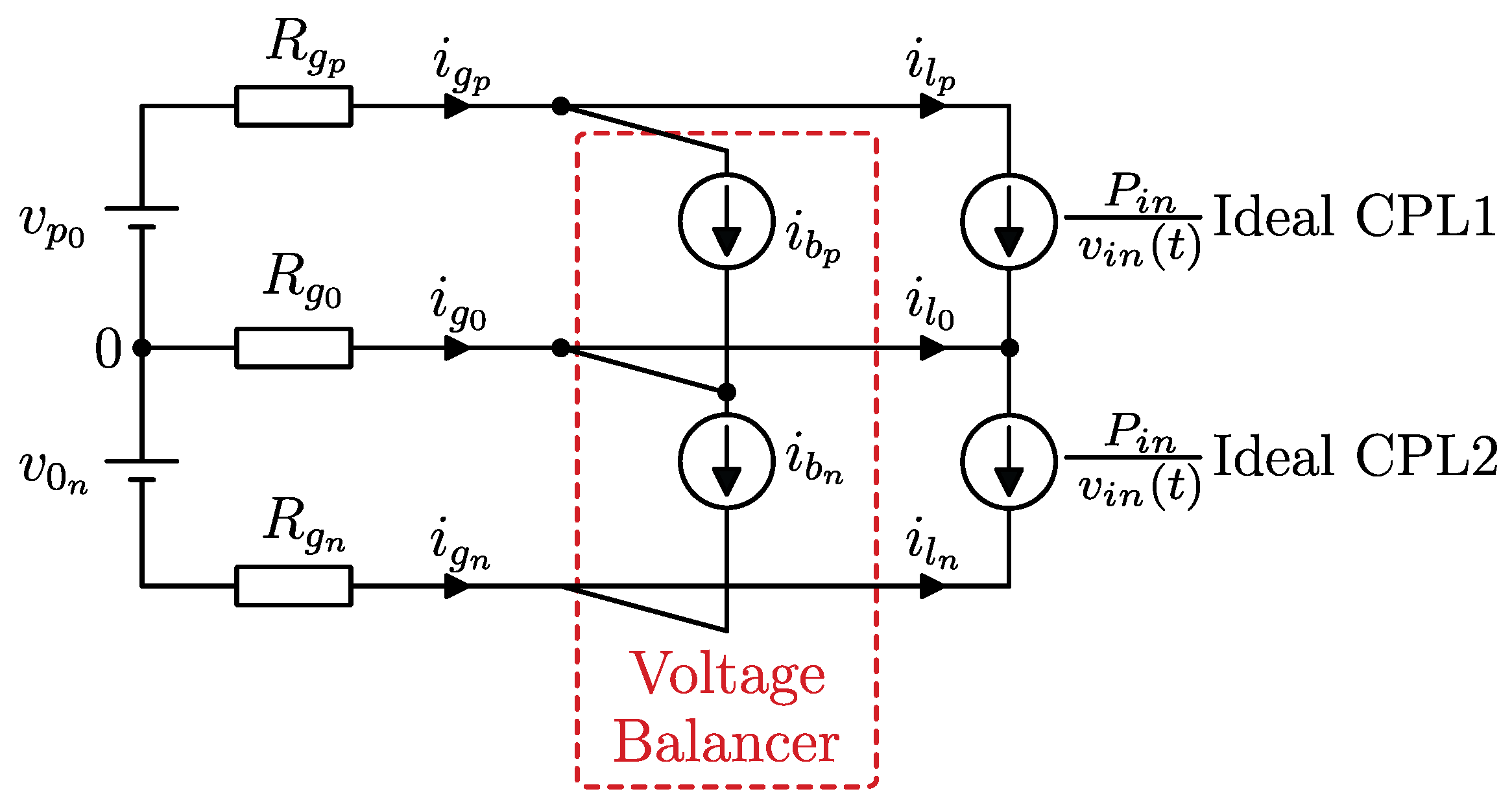
Figure 2 shows the equivalent circuit of a bipolar dc microgrid with a voltage balancer converter and two constant power loads (CPLs). The voltage balancer ensures that the neutral current i g 0 becomes zero when the branch currents i b p and i b n are equal.
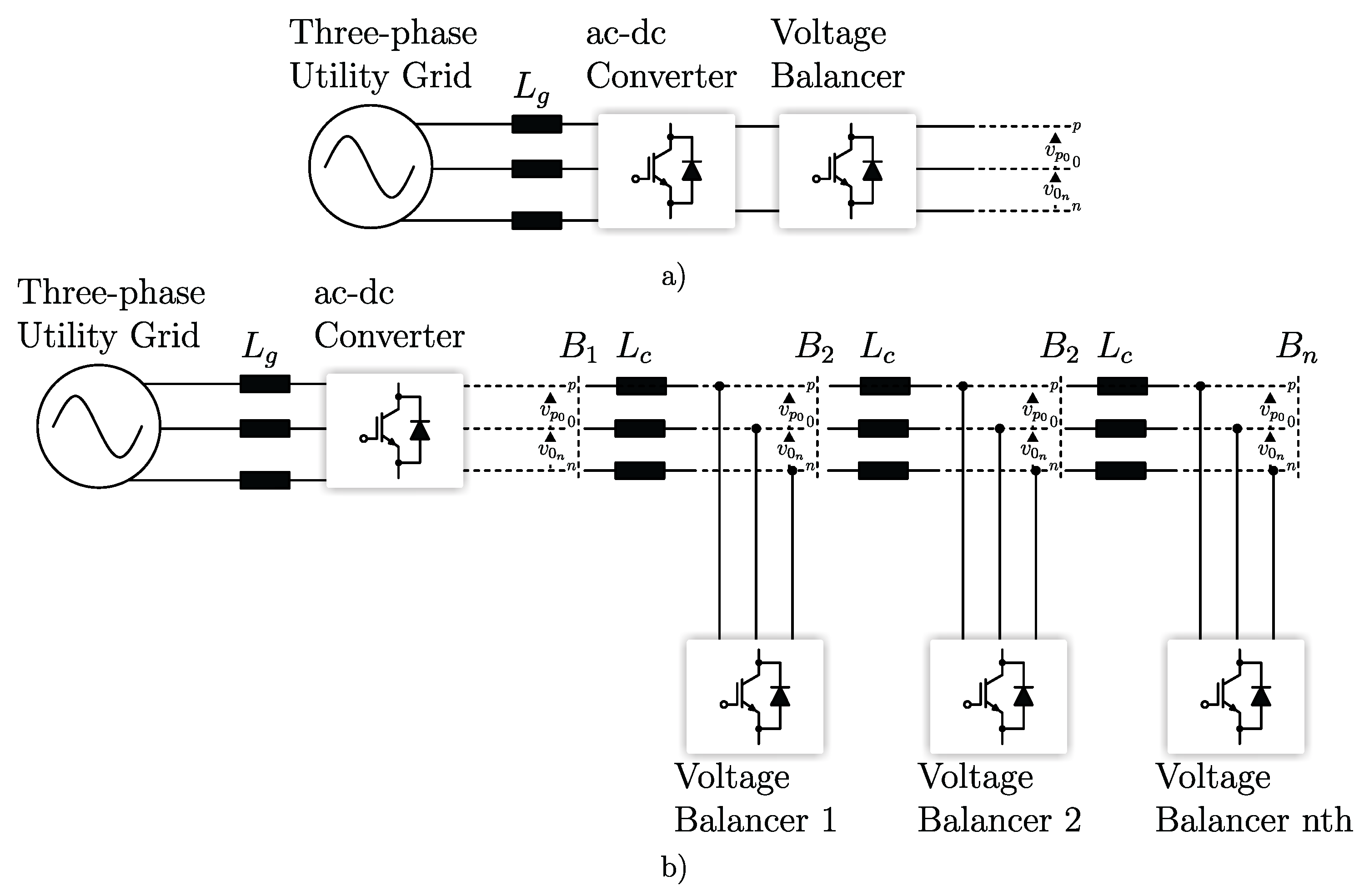
Figure 3 illustrates two voltage balancer configurations applied in bipolar dc microgrids. In Figure 3a, the centralized configuration is depicted, where a sufficiently large voltage balancer ensures bus voltage balancing. This approach is typically adopted in small-scale bipolar dc microgrids. Among the available topologies, the buck–boost converter is the most widely employed voltage balancer in centralized LVDC microgrids, owing to its simple structure and ease of control [20].
Figure 3b represents a bipolar dc microgrid with decentralized voltage balancers. In multi-mesh bipolar dc microgrids, the centralized approach may not be suitable, since long line connections can still result in asymmetric load voltages. In such cases, the decentralized strategy becomes more appropriate, with multiple voltage balancer converters distributed across the bipolar dc grid [24,25]. Various voltage balancer converters suitable for mitigating voltage unbalance issues in bipolar dc microgrids are presented in [26,27,28].
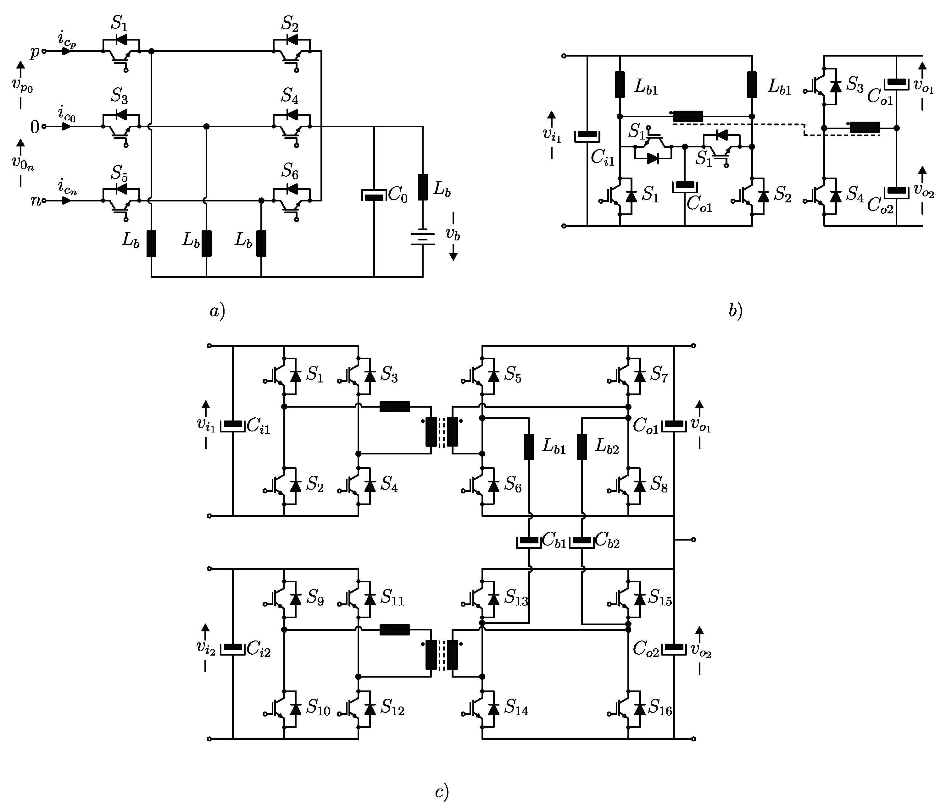
Figure 4 presents three representative configurations of voltage balancers suitable for bipolar dc microgrids. In Figure 4a, a solution employing a three-phase bidirectional buck–boost converter is illustrated, as reported in [29].
Whenever galvanic isolation is mandatory, isolated conversion stages can be incorporated into the voltage balancing architecture. In this context, the configuration depicted in Figure 4b utilizes a dual active bridge arrangement that establishes isolated and balanced dc outputs. Alternatively, Figure 4c displays an interleaved dual-boost-based voltage balancer, in which the design strategically exploits leakage and coupled inductances to support balancing functionality.
Furthermore, ref. [30] investigates voltage imbalance mitigation through coordinated operation and control of multiple dc zero-carbon buildings (DC-ZCBs) integrated into the microgrid infrastructure.
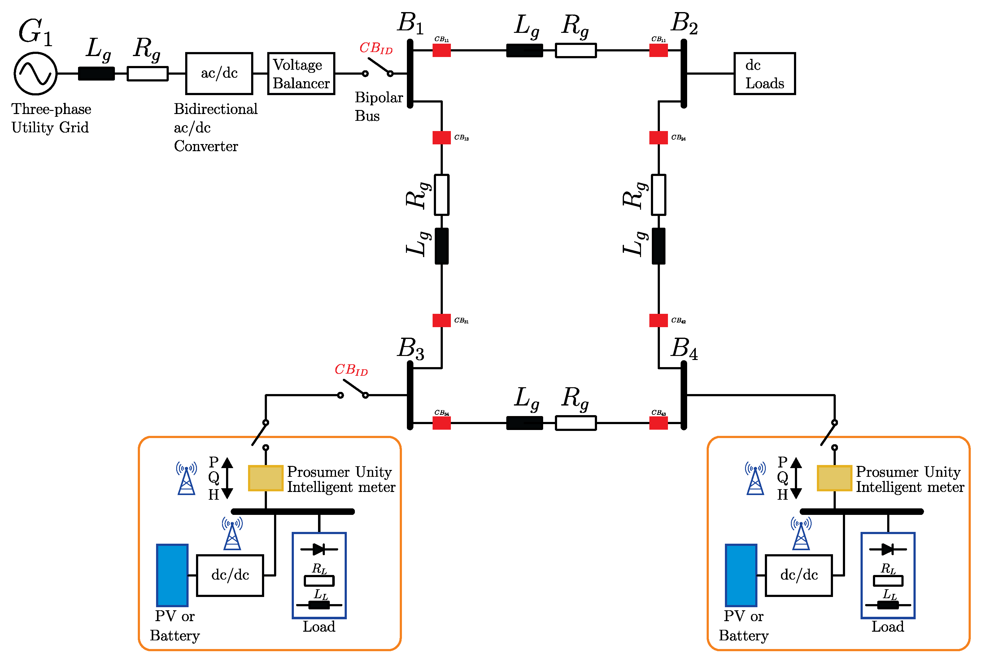
Bipolar dc architectures can have multi-bus and reconfigurable topologies [14]. An example of the latter is illustrated in Figure 5, where a ring-based dc microgrid configuration is presented. Such an arrangement enhances system reliability and operational redundancy, since multiple DER converters remain interconnected through the dc network. Additionally, the ring structure offers improved flexibility during fault events and scheduled maintenance, enabling sustained service continuity [14].
Unlike ac systems, dc microgrids do not present natural current zero-crossings, making them more vulnerable to severe pole-to-ground and pole-to-pole faults. These disturbances may result in excessive fault currents, potentially damaging power semiconductor devices if not promptly cleared. In [31], a rapid fault diagnosis strategy requiring a reduced number of sensors is introduced, relying on analytical fault modeling and frequency-response inspection of the system. Complementarily, ref. [32] proposes a coordinated control method aimed at mitigating voltage regulation issues inherent to dc ring microgrids.
In dc microgrids, droop control is utilized to regulate the dc bus voltage, enable current and power sharing among converters, and ensure proper operation under islanded conditions. Its main advantage is the facilitation of parallel operation among voltage-source converters.
Alternatively, master–follower strategies are also employed for bus regulation, where the master converter provides a large dispatchable capacity, while the follower converter operates as a complementary resource to enhance system reliability [33].
This paper proposes a bipolar dc microgrid composed of bidirectional dc power supply, a buck–boost voltage balancer, a low-voltage BESS connected to the 0–n node, a PV converter, and unbalanced electronic and resistive loads. The control architecture must ensure reliable operation in both grid-connected and islanded modes. The BESS converter employs the VI droop control method.
In the grid-connected mode, the BESS converter exchanges the required power with the main grid to recharge or discharge the battery bank, while the voltage balancer guarantees bus voltage balance. In the islanded mode, the BESS converter regulates the dc bus voltage v 0 n within a specified range, complying with the droop curve, and the voltage balancer operates as a voltage doubler to guarantee the balance of the intermediate v p 0 and v 0 n bus voltages.
For the droop controller of the BESS converter, unplanned islanding is seen as a load transient, enabling a seamless transition from grid-connected to islanded operation. However, voltage deviation is inherent to droop control.
This work addresses a comprehensive analysis of voltage balancing demonstrated in a bipolar dc microgrid under both grid-connected and islanded operating modes. The experimental results demonstrate effective voltage symmetry across the intermediate dc bus levels. By employing droop-based control in conjunction with the proposed voltage balancer strategy, the microgrid maintains reliable and stable operation even during islanded conditions.
This paper is organized as follows. Section 2 details bipolar dc microgrid architecture, Section 3 presents the control strategy of the microgrid. Section 4 shows the hardware setup, Section 5 shows operation modes of the microgrid and Section 6 details the experimental verification of the proposed bipolar dc microgrid approach. Section 7 concludes this paper.

2. Bipolar DC Microgrid Architecture

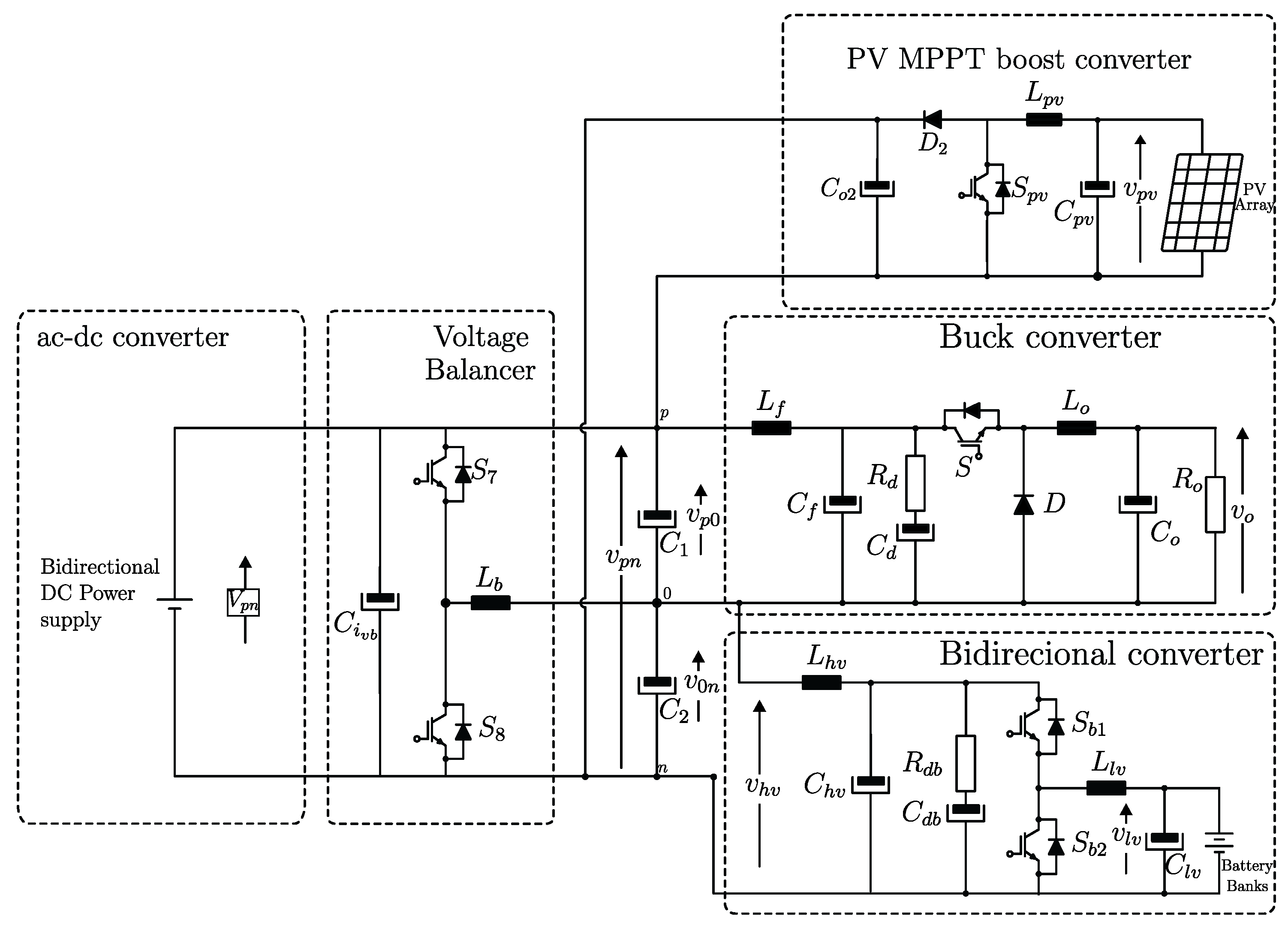
Figure 6 illustrates a bipolar DC microgrid composed of a photovoltaic (PV) system, a voltage balancer, a bidirectional dc power supply, a bidirectional converter, and a buck converter controlled to operate as a constant power load. The bipolar DC microgrid includes three DC bus poles: the total DC bus voltage v p n of 380 V, and the intermediate voltages v p 0 and v 0 n at ± 190 V.
The bidirectional dc power supply emulates an ac-dc bidirectional converter connected to a three-phase four-wire ac grid. The dc power supply is responsible for controlling the total DC bus voltage v p n at the 380 V reference. The voltage balancer maintains the balance between v p 0 and v 0 n even under unbalanced load conditions by providing a path for neutral current flow [23].
The bipolar dc microgrid must also coordinate the operation of DER converters connected to the bus. When the PV system generates surplus energy and injects current into the pn pole, the system must export the excess current to the ac grid.
Furthermore, both unidirectional and bidirectional dc–dc converters can be connected to the 380 V bipolar dc bus or to the intermediary buses ( ± 190 V). These converters enable the generation of LVDC voltage levels (96 V, 48 V, 24 V, 12 V) for residential or commercial applications, as well as the integration of renewable energy systems such as battery banks and EV chargers.

3. Control Strategy of the Microgrid

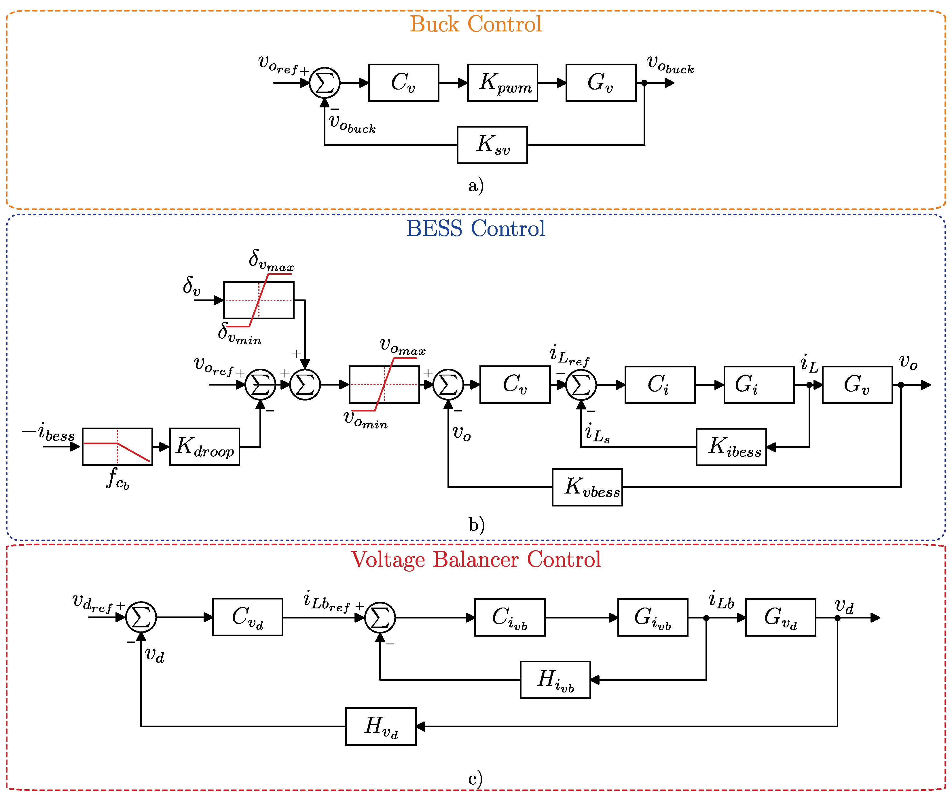
Figure 7 shows the complete control system of the bipolar dc microgrid. Figure 7a displays the control block diagram of the buck converter, where K P W M denotes the modulator gain and K s v the voltage sensor gain.
The design of the lead–lag compensator follows [34,35]. Equation (1) presents the transfer function relating the output voltage v o and the duty cycle d b u c k . L o , C o and R o denote the output inductance, output capacitance, and equivalent load resistance of the converter, respectively.
G v o ( s ) = v ^ o d ^ b u c k = V p 0 s 2 · L o · C o + s · ( L o / R o ) + 1 .
Equation (2) describes the lead–lag PID controller, including a high-frequency filter to avoid saturation of the derivative gain. This PID controller is designed to achieve a crossover frequency of 535 Hz and a phase margin of 75.5°. The lead-lag poles and zeros are described in Table 1.
G b u c k = k P D · 1 + ω L s · 1 + s ω z 1 + s ω p · 1 1 + s ω p 2 .
Figure 7b displays the control block diagram of the droop-controlled BESS converter considered in this work. The small-signal model of a generic droop-controlled boost converter is described in [36]. In this work, a single low-voltage (95 V) BESS converter under droop control is proposed and connected to one of the intermediate buses (p–0 or 0–n). This configuration enables reliable and seamless operation of the bipolar DC microgrid in both grid-connected and islanded modes, leveraging the plug-and-play capability of droop control.
Equation (3) presents the transfer function relating the bess inductor current i b e s s and the duty cycle d. L o d , C o 1 , and D p represent the output inductance, output capacitance, and static duty cycle of the converter, respectively. V o d and I o d are the output voltage and the output current, respectively.
G i b e s s d ( s ) = i ^ b e s s d ^ = s C o 1 · V o d + I o d s 2 L o d C o d + ( 1 D p ) 2 .
Equation (4) presents the transfer function relating the output voltage and the BESS inductor current. V D G and I l d represent the battery voltage and the inductor current.
G v o d i L d ( s ) = v ^ o d i ^ l d = s L o d I L d + V D G s C o d C o d + I o d .
The V-I droop control technique may be implemented using only the inductor current feedback. In this technique, the inductor BESS current is filtered by a low-pass filter (crossover frequency of f c b ), then multiplied by the droop resistance K d r o o p , and subsequently injected into the voltage control loop.
Equation (5) details the transfer function that relates the inductor current and the output current. Considering the low-pass filtering of the BESS inductor current i b e s s , the transfer function between inductor current and output current can be approximated.
G i l d i o d ( s ) = i ^ l d i ^ o d = 1 D p s 2 L o d C o d + ( 1 D p ) 2 1 ( 1 D p ) = 1 d .
Therefore, the droop resistance K d r o o p is described in Equation (6).
K d r o o p = r d · d .
Equation (7) shows the voltage reference of the droop control. In this system, V o is the no-load voltage reference. The voltage droop is achieved by multiplying the droop coefficient K d r o o p by the BESS inductor current i b e s s . The voltage term δ v is utilized depending on the microgrid operation mode. In grid-connected mode, δ v is used to recharge/discharge the battery bank. In the islanding scenario, δ v can be utilized to the dc bus restoration at the nominal voltage.
V o r e f e r e n c e = V o K d r o o p i b e s s + δ v .
Figure 7c shows the control block diagram of the voltage balancer [23], where H v d denotes the voltage sensor gain and H i v b current sensor gain. C i v b denotes the internal PI current controller, while C v d regulates the differential voltage.
The voltage balancer maintains the balance between the voltages v o 1 and v o 2 by providing a current path between the positive and negative poles. The control system must ensure that the differential voltage is zero ( v d = v p 0 v 0 n = 0 ). The voltage deviation percentage in the bipolar dc microgrid is defined by (8). Since no standardized limit exists for bipolar dc microgrids, a maximum value of 5% is adopted in this work.
Δ U V = 2 × v p 0 v 0 n v p n × 100 % .
Equation (9) details the transfer function relating the inductor current i L b to the duty cycle d v b [23], where a PI controller is tuned to achieve a 90° phase margin and a crossover frequency of 1200 Hz. V o , L b , and R L b represent the output voltage, inductance, and inductor parasitic resistance, respectively.
G i v b ( s ) = i ^ L b d v b ^ = 2 · V o s · L b + R L b .
Equation (10) shows the transfer function between the differential voltage and the inductor current of the voltage balancer [23], with control parameters set for a 90° phase margin and a 120 Hz crossover frequency. Table 1 shows the experimental control parameters. R o 1 and C represent the output resistance and capacitance of the bus, respectively.
G v d ( s ) = v d ^ i ^ L b = 3 · R o 1 s · R o 1 · C + 1 .

4. Hardware Experimental Setup

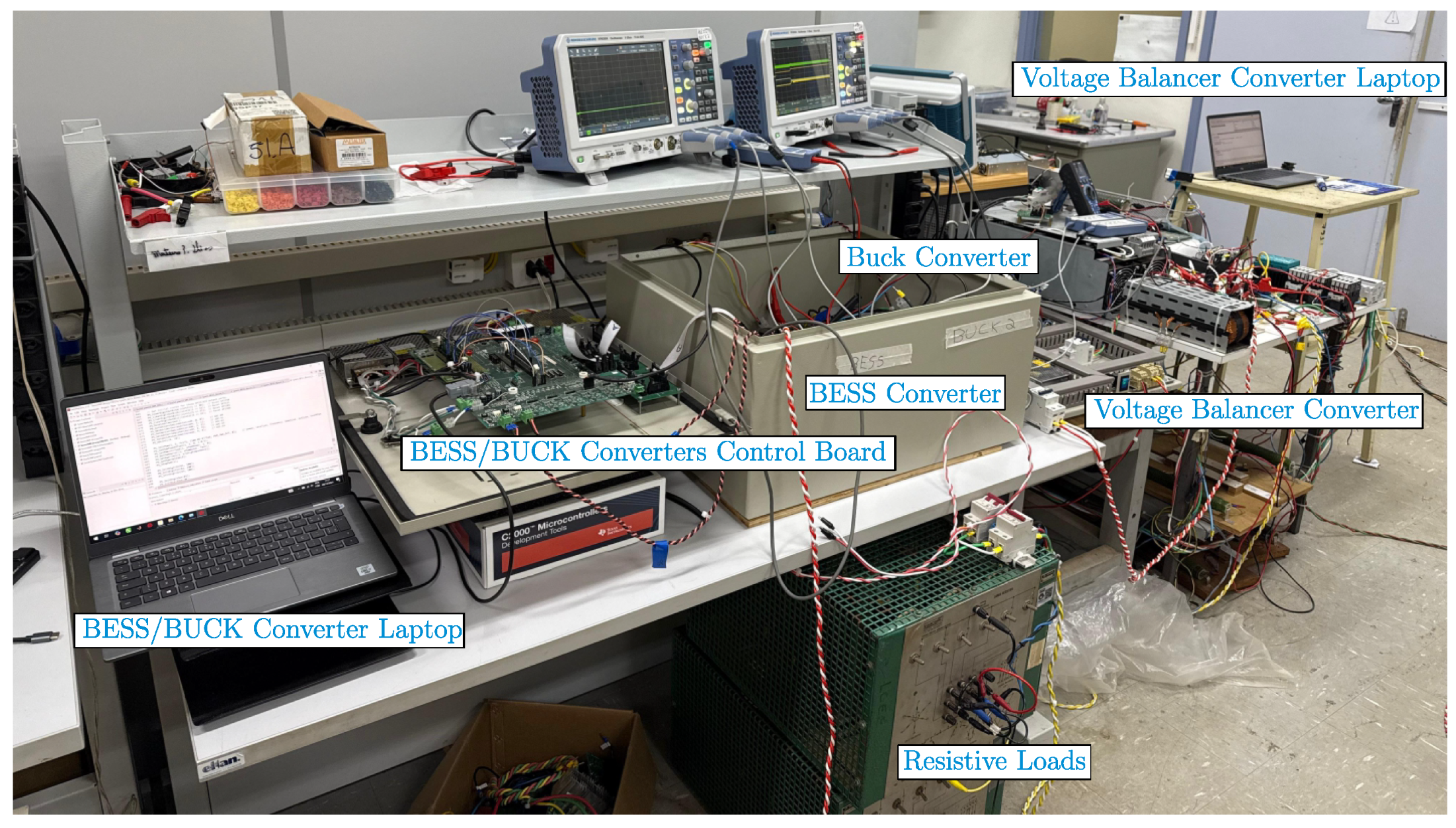
Figure 8 presents the experimental prototype of the bipolar dc microgrid developed at the Power Conditioning Laboratory (LCEE) located at the State University of Campinas (UNICAMP), Brazil.
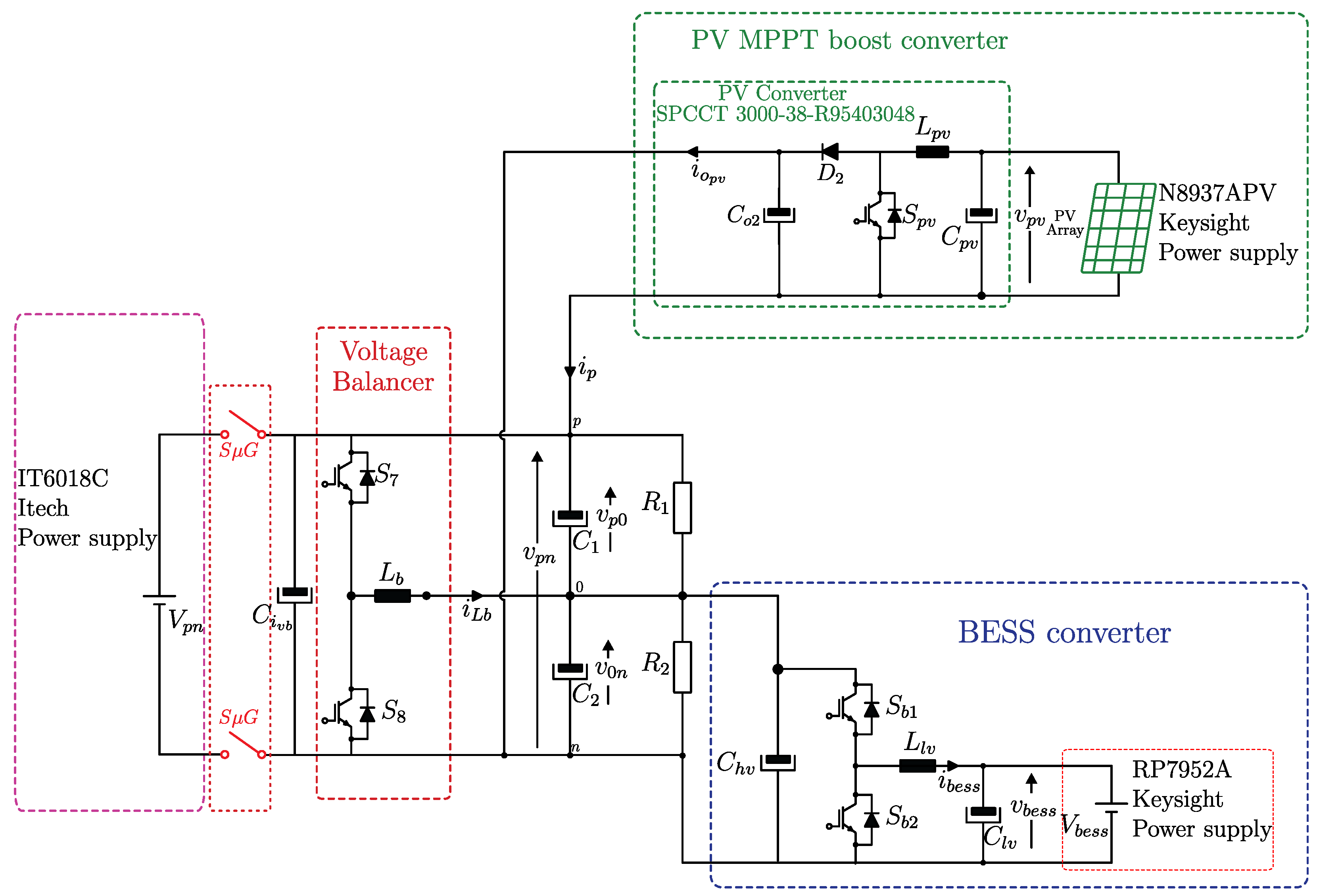
Figure 9 illustrates the experimental setup, which consists of a dc–dc converter box (including a buck converter and a BESS converter), a voltage balancer converter, and resistive loads. In the operating scenarios, the ac–dc converter is emulated by a bidirectional dc power supply.
The bidirectional dc power supply is the ITECH ® IT6018C model. This dc power supply regulates the 380 V total dc bus voltage v p n . The 95 V battery bank is emulated with the dc power supply RP7952A Keysight ® regenerative power system.
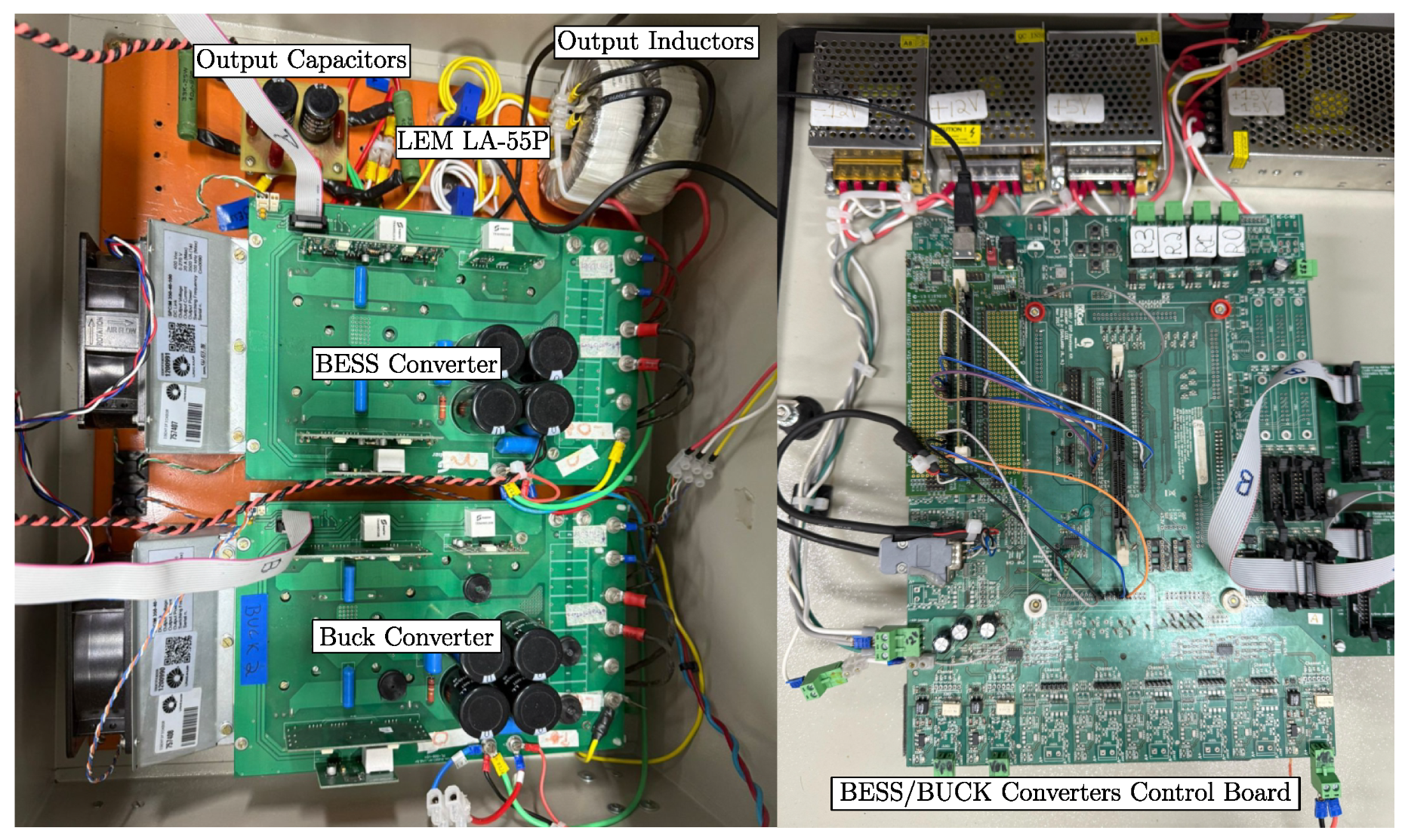
Figure 10 shows the assembled BESS converter and buck converter along with the control board. The BESS converter and the buck converter are implemented using two SPCIM 350-40-100® two-leg converter modules. Table 2 presents the analog conditioning gains for the output voltage v 0 and the BESS current i b e s s .
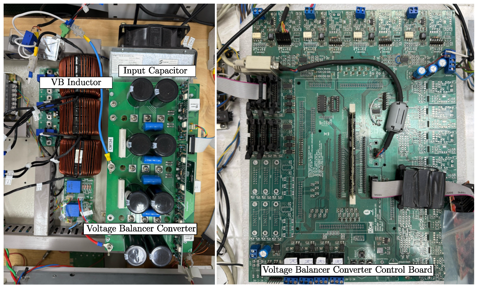
Figure 11 illustrates assembled voltage balance converter and its control board. The voltage balance converter is implemented with the SPMIT 750-50-20 Supplier® three-leg converter module. Table 3 presents the analog conditioning gains for the intermediary voltage v p 0 and the voltage v 0 n .
The control platform is a Texas Instruments TMS320F28335 DSP Control Card. Control parameters and the serial communication firmware are generated in PSIM and compiled using Code Composer Studio. The voltage measurement utilizes HCPL-7510 amplifiers, the current measurement employs 55P LEM Hall-effect sensors, and each channel has a 12 kHz anti-aliasing filter.
The complete system parameters are described in the following tables. Table 4 summarizes the microgrid and voltage balancer parameters. Table 5 summarizes the BESS converter and buck parameters. Table 6 summarizes the PV parameters.

5. Operation Modes of the Bipolar DC Microgrid

A dc microgrid must ensure reliable operation both when connected to the dc grid-forming source and during islanded mode with smooth transitions between them. The details of the operation of the proposed system in these two operation modes are described in this section, along with the adopted strategy to ensure smooth transition in front of an unintentional islanding event in the microgrid.
  • Mode A: Microgrid operating grid-connected to the dc former
During grid-connected operation, the dc grid former converter functions as a voltage source, regulating the 380-V v p n bipolar dc bus. The voltage balancer actively maintains the voltage symmetry between the intermediate buses, v p 0 and v 0 n . Meanwhile, the BESS converter provides bidirectional power exchange to support battery charging and discharging, operating as a current-controlled source under this condition.
The charging and discharging actions are governed by the parameter δ v . Positive values of δ v correspond to battery charging, whereas negative values indicate discharging. Variations in the BESS voltage reference introduce dynamic voltage deviations into the system.
The voltage balancing performance of the microgrid is analyzed in the next section. Initially, an unbalanced resistive load is applied to the microgrid, and the voltage balancer is required to ensure overall bus voltage balance. Furthermore, an electronic load is subsequently introduced into the microgrid, and its impact on voltage unbalance is evaluated. The behavioral differences between these two loading conditions are presented and discussed.
  • Mode B: Microgrid operating islanded
During islanded operation, the dc grid former converter is electrically isolated from the bipolar dc microgrid by opening the switch S μ G . In this condition, the BESS converter assumes the primary responsibility for regulating the lower bus voltage, v 0 n , within the specified operational limits. Simultaneously, the voltage balancer operates as a voltage-doubling stage, thereby maintaining proper voltage symmetry between the intermediate buses v p 0 and v 0 n .
Through coordinated control, the BESS converter and the voltage balancer collectively ensure adequate load supply capability, reliable standalone operation of the microgrid, and sustained voltage balance across the bipolar dc network.
  • Seamless transition from Mode A to Mode B
When the dc grid former is disconnected from the microgrid, the droop-controlled BESS seamlessly assumes the voltage regulation role, enabling a smooth transition from grid-connected to islanded operation, inherently supporting plug-and-play functionality. From the droop controller’s perspective, this unintentional disconnection works as a sudden load variation. By adapting its operating point accordingly, the droop control mechanism maintains stable voltage regulation, thus preserving the reliable operation of the bipolar dc microgrid.
In the next section, the experimental results demonstrate the seamless transition from mode A (grid-connected) to mode B (islanded operation). The voltage balancing performance of the microgrid, as well as the effectiveness of the droop control, are evaluated. Moreover, the presented results confirm the complete and reliable operation of the bipolar dc microgrid.

6. Bipolar DC Microgrid Experimental Results

In this work, the dc bus voltages v p 0 and v n 0 range between ± 180 V to ± 210 V, resulting in maximum and minimum voltages of 420 V and 360 V between the dc bus poles. These maximum and minimum values limit the range of the droop curve used in the BESS converter. Initially, the voltage balancing of the bipolar microgrid is tested under unbalanced resistive and electronic loads.
The following subsections bring the following content:
  • Section 6.1 shows the voltage balancer entering operation in open-loop.
  • Section 6.2 illustrates the resistive loads vary, perturbing the balance of the bipolar dc bus.
  • Section 6.3 brings the results of the voltage balancer operating in closed-loop.
  • Section 6.4 introduces electronic loads, known for affecting the stability of electrical systems.
  • In Section 6.5, the balancer operates in closed-loop, with electronic loads in the system, keeping its stability.
  • Section 6.6 presents the results of the balancer within and islanded operation.
  • Finally, Section 6.7 qualitatively summarizes the experimental results.
The following experimental results are based on the measurement of the voltage imbalance between the intermediate voltages v p 0 and v 0 n . Regardless of the imbalance condition, the system must continue operating within the voltage limits. Therefore, the first experiments demonstrate the necessity of the balancer operating in closed-loop.The results presented in Section 6.1, Section 6.2, Section 6.3, Section 6.4 and Section 6.5 correspond to the grid-connected operating condition (Mode A). In Section 6.6, the microgrid seamlessly transitions from the grid-connected to the islanded condition and continues operating under Mode B (islanded mode).

6.1. Voltage Balancer Entering Operation

In mode A (grid-connected operation), the ITECH dc power supply regulates the 380 V bipolar dc bus voltage v p n . The voltage balancer ensures the balance of the intermediate bus voltages v p 0 and v 0 n . The BESS converter uses the V–I droop control method, recharging and discharging the battery bank to exchange the required power.
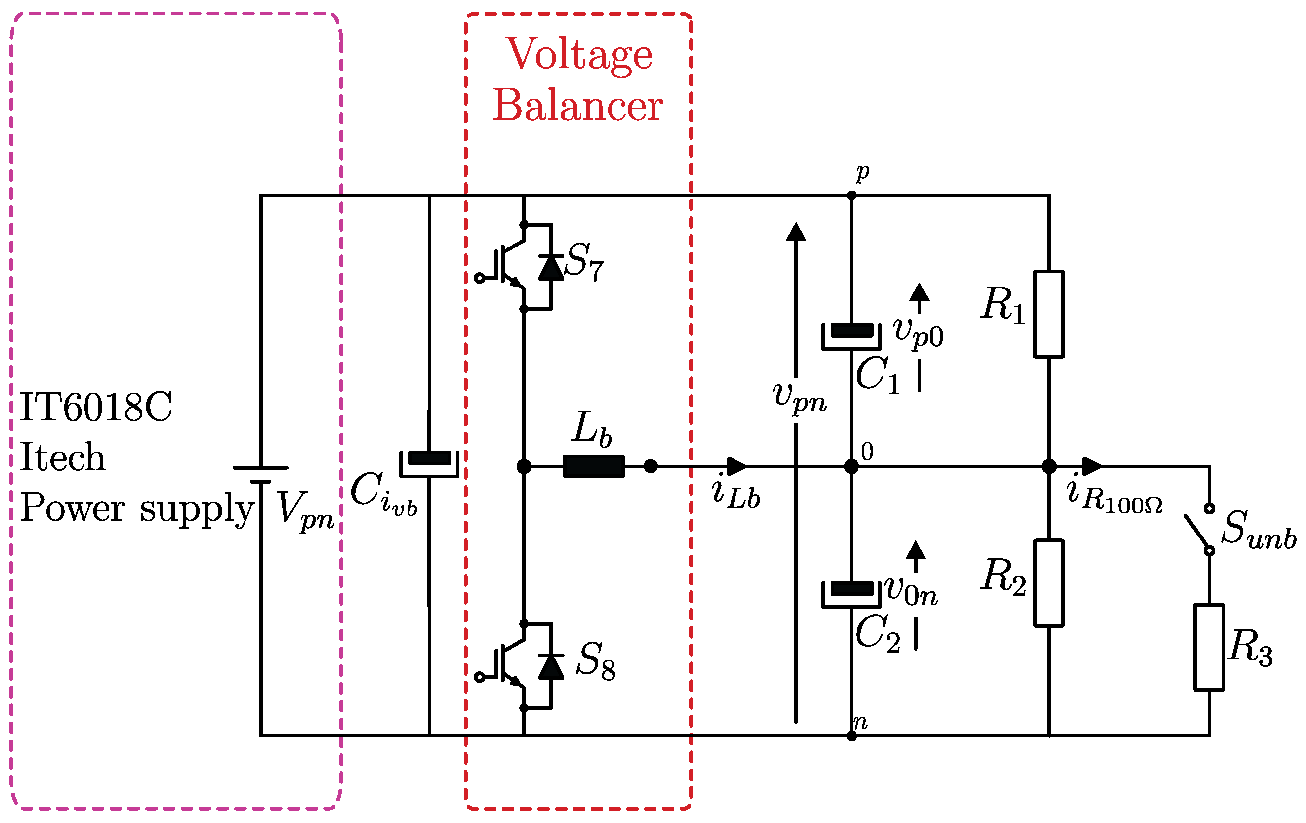
Figure 12 illustrates the equivalent circuit of the scenario analyzed. The resistances are given as R 1 = 88 Ω , R 2 = 150 Ω , and R 3 = 100 Ω . When the switch S u n b is closed, the equivalent resistance at the 0–n node is calculated as R e q = R 2     R 3 = 60 Ω .
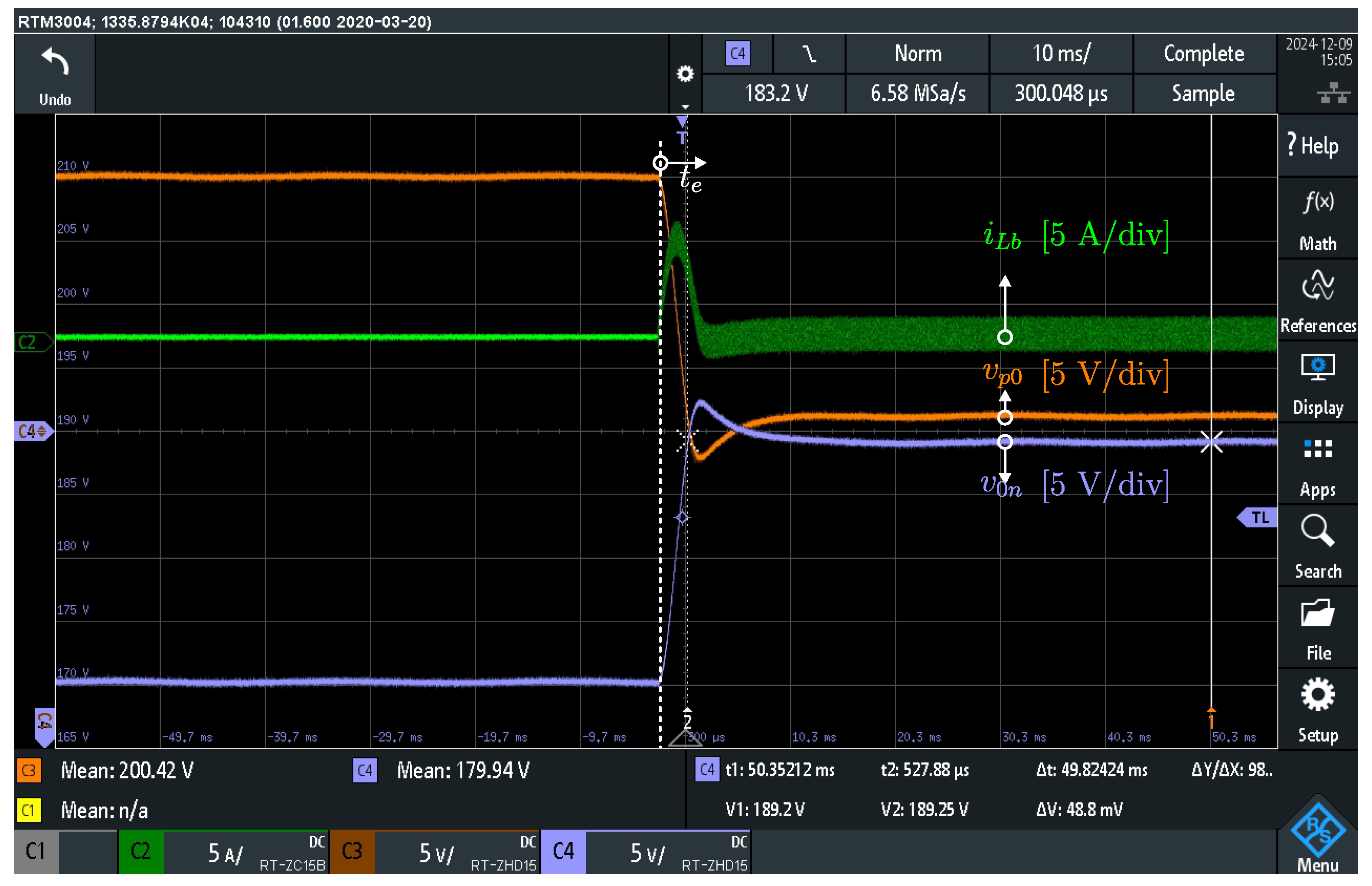
Figure 13 illustrates the transient response of the bipolar dc microgrid when the voltage balancer is activated under an unbalanced load condition. Channel 2 presents the voltage balancer current i L b (green trace, 5 A/div), Channel 3 presents the 190 V node voltage v p 0 (orange trace, 5 V/div, offset: 190 V), and Channel 4 presents the 190 V node voltage v 0 n (light blue trace, 5 V/div, offset: 190 V).
The experimental results are organized before and after the connection of the voltage balancer in t e .
Before t e , the dc power supply ensures the 380 V pole-to-pole bipolar dc bus, the voltage balancer is detached, and the intermediary voltages are unbalanced. The v 0 n voltage is 170 V and the v p 0 is 210 V, resulting in a voltage deviation of approximately 40 V ( Δ U V = 21 % ). This voltage deviation depends on the respective bus loading conditions.
The voltage balancer is activated with a fixed duty cycle of 0.5 at t e . After 15 ms, the balancer regulates the voltages v p 0 and v 0 n reducing and the voltage deviation to approximately 3 V ( Δ U V 1.66 % ). The experimental results demonstrate that the voltage balancer maintains the voltage balance under unbalanced loading conditions. Because of this feature, this converter is essential for a bipolar dc microgrid.

6.2. Voltage Balancer Responding to Load Variations

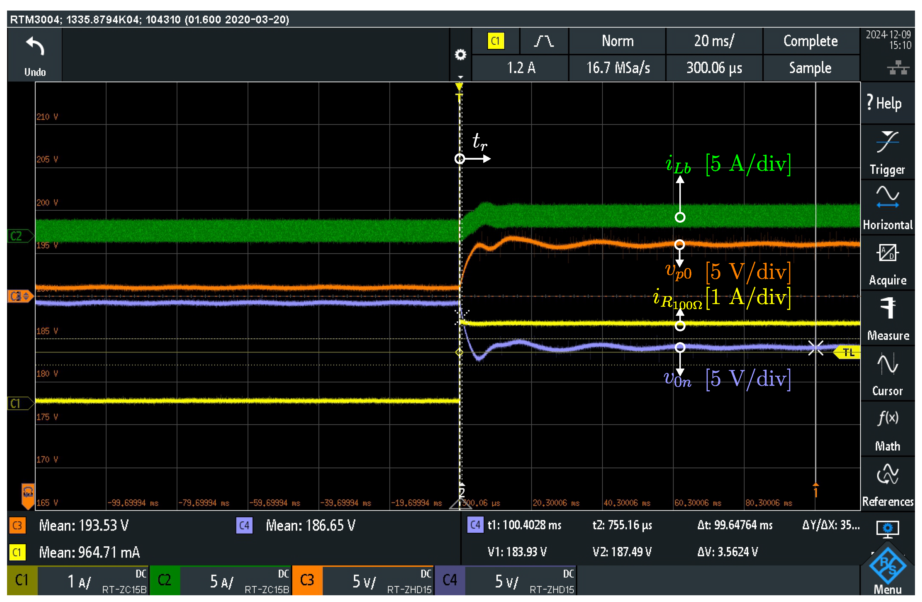
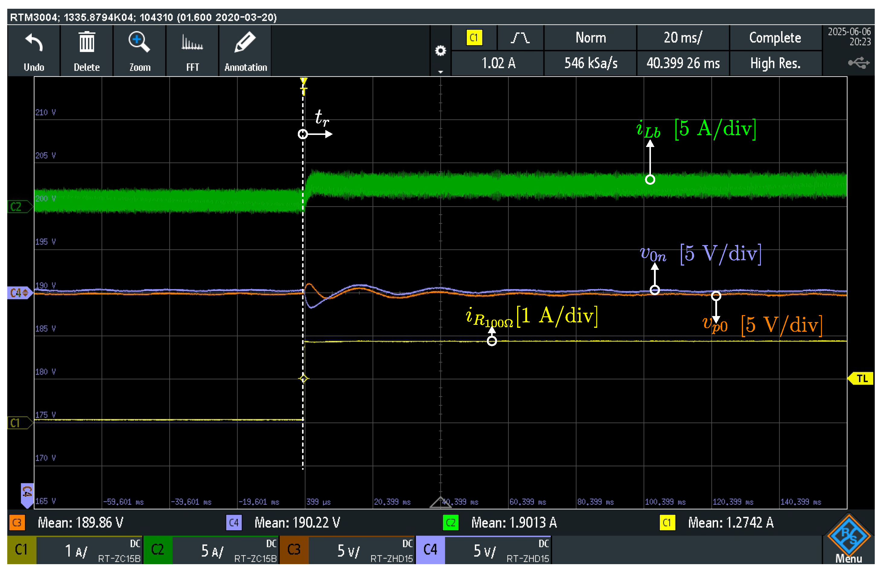
To evaluate the dynamic response of the system to load variations, a resistive load step of 100 Ω perturbs the 0–n dc bus. Figure 14 illustrates the transient response of the bipolar dc microgrid to this event.
Channel 1 presents the load current i R 100 Ω (yellow trace, 1 A/div), Channel 2 presents the voltage balancer current i L b (green trace, 5 A/div), Channel 3 presents the 190 V node voltage v p 0 (orange trace, 5 V/div, offset: 190 V), and Channel 4 presents the 190 V node voltage v 0 n (light blue trace, 5 V/div, offset: 190 V).
Before t r , the voltage balancer maintains the balance of the bipolar dc bus voltages, with a deviation of approximately 3 V ( Δ U V 1.6 % ). At t r , a 100 Ω resistive load is connected to the 0–n dc bus in parallel with the R 2 . After 40 ms, the voltages v p 0 and v 0 n stabilizes, exhibiting a deviation of approximately 12 V ( Δ U V = 6.3 % ). This increased deviation results from the open-loop operation of the voltage balancer with a fixed duty cycle of 0.5 . Since Δ U V exceeds the 5 % maximum unbalance adopted, closed-loop control of the voltage balancer is required.

6.3. Closed-Loop Voltage Balancer

In open-loop mode, the voltage balancer cannot compensate for the increased voltage deviation that happens due to load imbalance. To mitigate the voltage deviation, the voltage balancer operates in closed-loop mode to ensure the balance between v p 0 and v 0 n . The resistances are defined as R 1 = 176 Ω and R 2 = 150 Ω .
Figure 15 illustrates the transient response of the bipolar dc microgrid under a resistive load step of 100 Ω applied at the 0–n dc bus.
Channel 1 presents the load current i R 100 Ω (yellow trace, 1 A/div), Channel 2 presents the voltage balancer current i L b (green trace, 5 A/div), Channel 3 presents the 190 V node voltage v p 0 (orange trace, 5 V/div, offset: 190 V), and Channel 4 presents the 190 V node voltage v 0 n (light blue trace, 5 V/div, offset: 190 V).
Before t r , the voltage balancer regulates the bipolar dc bus voltages, reducing the deviation to approximately 0.5 V ( Δ U V = 0.26 % ). At t r , a 100 Ω resistive load is connected to the 0–n dc bus in parallel. After 40 ms, the voltage balancer equalizes again the voltages v p 0 and v 0 n . Therefore, the closed-loop operation of the voltage balancer effectively guarantees the stability and minimizes the voltage deviation of the intermediate bus voltages.
The importance of employing a closed-loop technique for the balancer control in a microgrid is emphasized based on Table 7. The comparison between Section 6.1, Section 6.2 and Section 6.3 is carried out considering the imbalance level of each test. In the case of open-loop operation, depending on the load step, the system may operate outside the limits defined by the droop curve. Such a condition can be highly detrimental to the equipment connected to the microgrid, potentially leading to failures or even complete system malfunction.
Assuming a maximum imbalance condition in the system and with the balancer operating in open-loop, an electronic load whose rated operation depends on the defined voltage limits may fail to operate properly.

6.4. Load Converter Experimental Setup: Voltage Balancer in Open-Loop and the Transient Response Due to Load Step

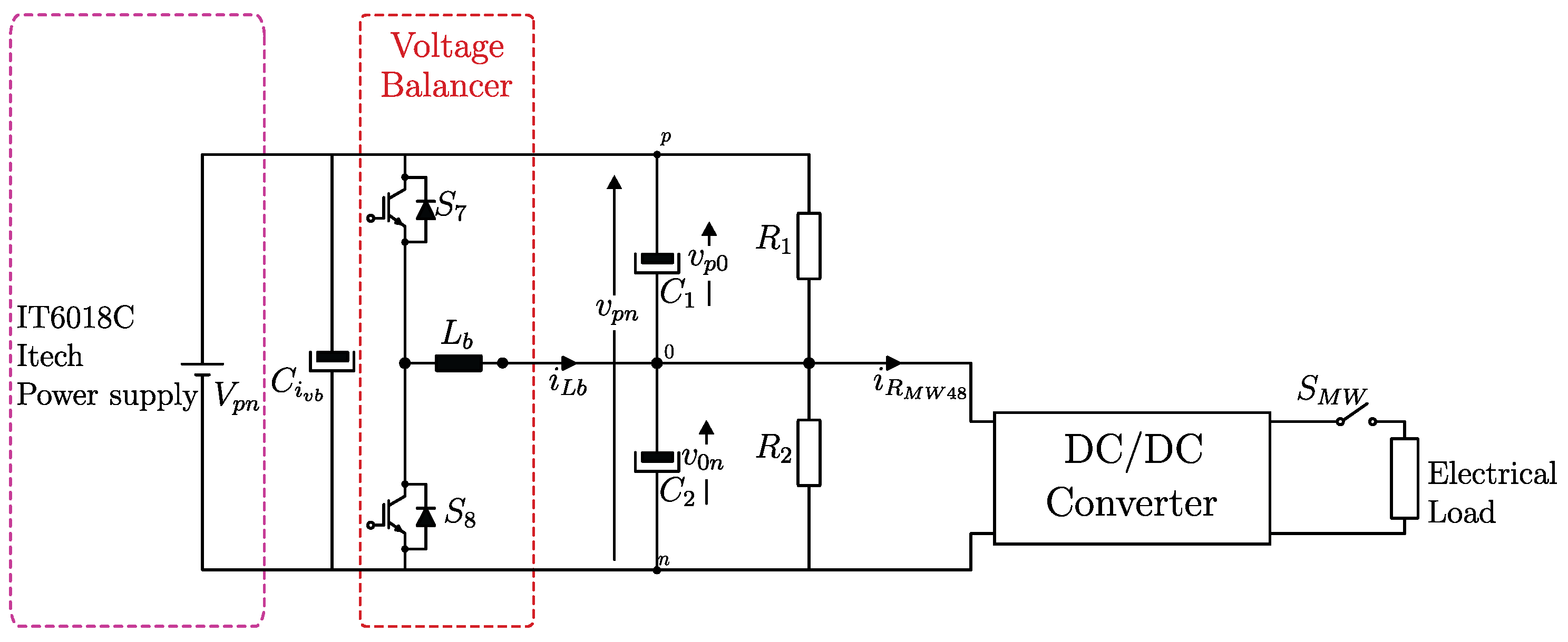
The load converter is implemented using the RSP-1000-48 module (Mean Well®). The load converter operates with an input voltage of 190 V, an output voltage of 48 V, and a rated power of 1 kW.
Figure 16 presents the equivalent circuit including the load converter, where R 1 = 176 Ω and R 2 = 150 Ω .
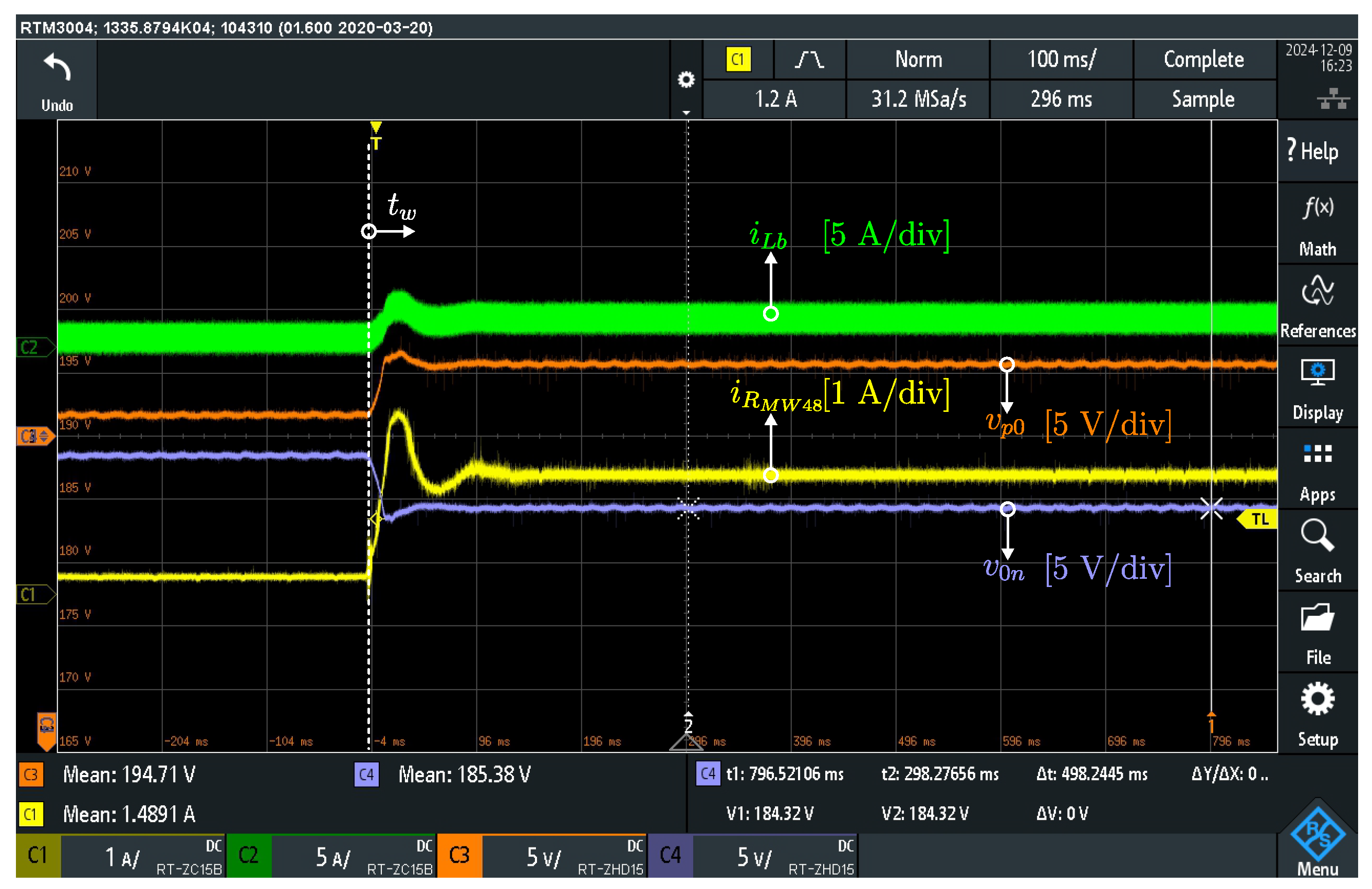
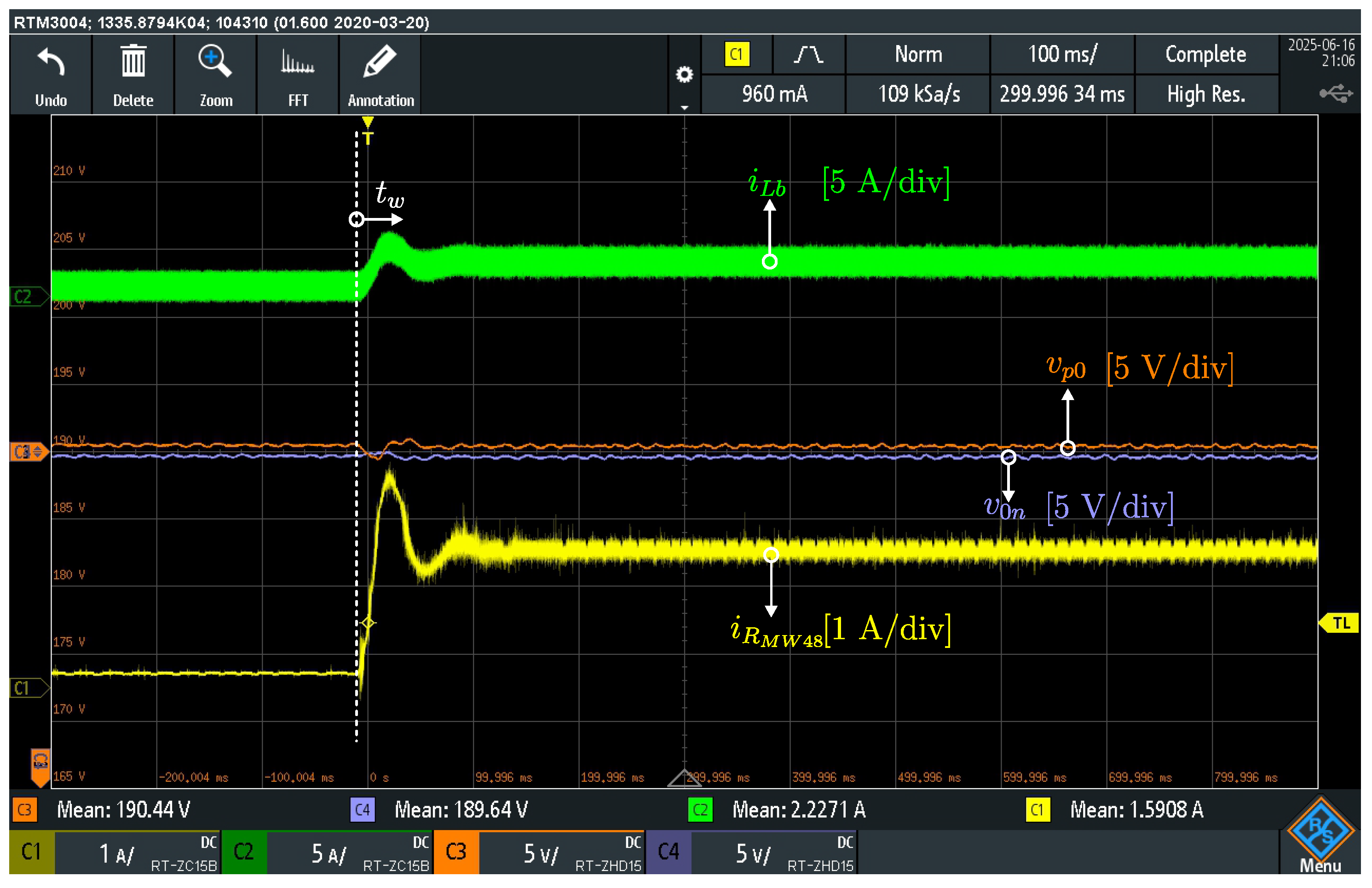
Figure 17 illustrates the dynamic behavior of the microgrid when the load converter is connected to the 0–n dc bus.
Channel 1 presents the load converter current i R M W 48 (yellow trace, 1 A/div), Channel 2 presents the voltage balancer current i L b (green trace, 5 A/div), Channel 3 presents the voltage v p 0 (orange trace, 5 V/div, offset: 190 V), Channel 4 presents the voltage v 0 n (light blue trace, 5 V/div, offset: 190 V).
At t w , the switch S M W closes and the load converter is connected to the 0–n dc bus. After approximately 100 ms, the intermediary bus voltages v p 0 and v 0 n reach balance, with a voltage deviation of about 12 V ( Δ U V = 6.3 % ). In this condition, the input current of the load converter, i R M W 48 , is approximately 2 A.
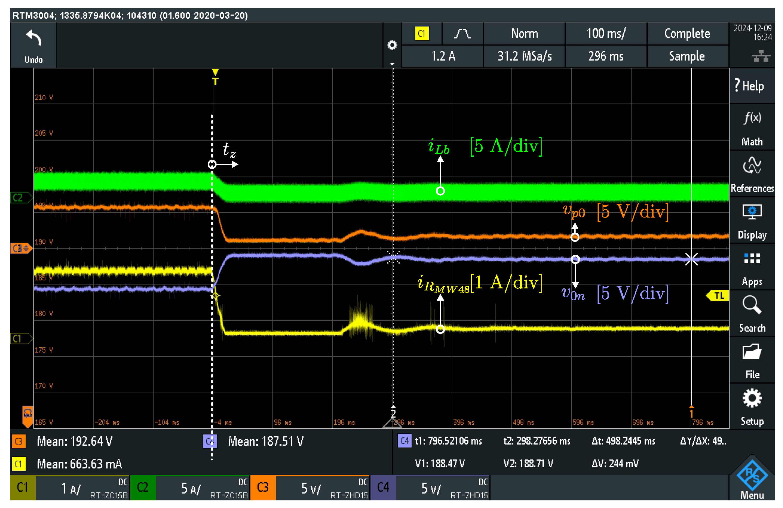
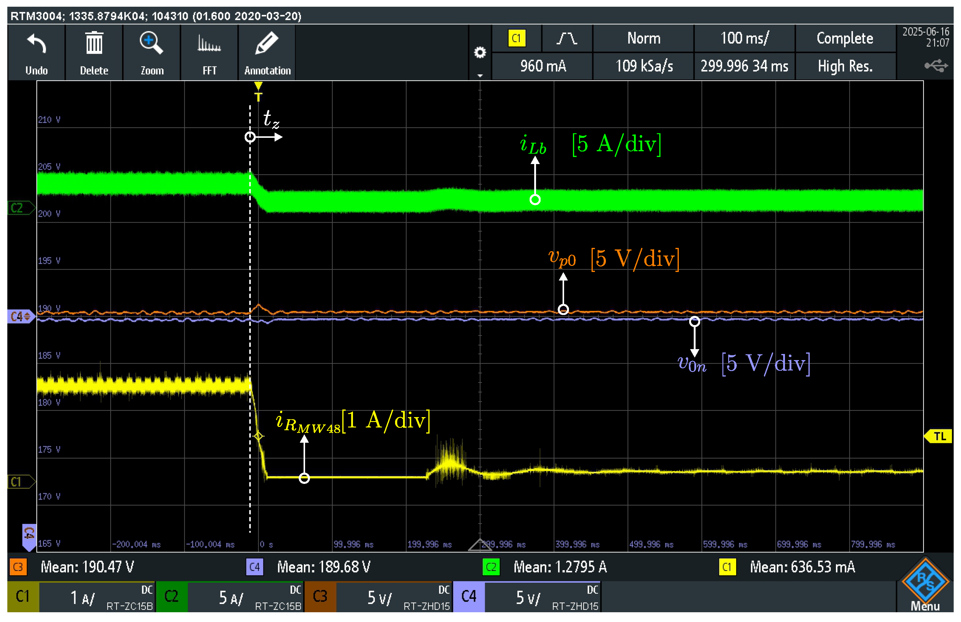
Figure 18 illustrates the transient response corresponding to the disconnection of the load converter from the 0–n dc bus. At instant t z , the switch S M W opens. Therefore, after 100 ms, the voltage deviation decreases to approximately 3 V ( Δ U V = 1.6 % ).

6.5. Load Converter Experimental Setup: Closed-Loop Voltage Balancer and the Transient Response Due to Load Step

To guarantee the voltage balancing of the intermediary voltages even with unbalanced load steps, the voltage balancer is operating in closed-loop. The resistances connected to the bipolar bus are R 1 = 176 Ω and R 2 = 150 Ω .
Figure 19 illustrates the transient response observed during the connection of the load converter to the 0–n dc bus.
Channel 1 presents the load converter current i R M W 48 (yellow trace, 1 A/div), Channel 2 presents the voltage balancer current i L b (green trace, 5 A/div), Channel 3 presents the bus voltage v p 0 (orange trace, 5 V/div, offset: 190 V), and Channel 4 presents the bus voltage v 0 n (light blue trace, 5 V/div, offset: 190 V).
At t w , the switch S M W closes, and the load converter is connected to the 0–n dc bus. After approximately 100 ms, the intermediary bus voltages v p 0 and v 0 n reach balance, with a voltage deviation of about 0.8 V ( Δ U V = 0.42 % ). In this condition, the input current i R M W 48 is approximately 2 A.
Figure 20 illustrates the transient response corresponding to the disconnection of the 48 V converter from the 0–n dc bus. At instant t z , after 100 ms, the dc bus voltage deviation is again approximately 0.8 V ( Δ U V = 0.42 % ).
In closed-loop mode, the voltage balancer ensures the balance of the intermediary voltages. This converter maintains a voltage unbalance below 5 % during transients and keeps the dc microgrid compliant with the droop voltage range.
The dynamic performance of the load converter contrasts with that of the resistive load. Specifically, the input current of the load converter has an oscillatory dynamic behavior, whereas the resistive load displays a damped response. In practical applications of dc microgrids, considering that all loads are inherently electronic and have input dynamic characteristics that are more similar to those of the load converter. Therefore, the dc bus must ensure adequate reliability to guarantee that the frequent connection and disconnection of such loads does not affect the system.
Furthermore, Table 8 presents a comparison of a load step applied to the load converter when the balancer operates in open-loop and its corresponding response under closed-loop operation. The comparison between Section 6.1, Section 6.2 and Section 6.3 is carried out considering the imbalance level of each test.
To provide a clearer understanding of this relationship between the systems, the responses presented in Table 7 and Table 8 can be compared. The microgrid must be able to withstand the oscillatory behavior induced by the load step at the load converter input. Thus, it is observed that the proposed control for the voltage balancer ensures reliable operation during the tests performed under microgrid operating mode A.

6.6. Unplanned Island Scenario

In this section, the dynamic behavior of the microgrid is evaluated under an unplanned islanding event of the dc grid-forming converter when the S μ G , shown in Figure 9, opens. The load resistances are set to R 1 = 176 Ω and R 2 = 150 Ω .
The droop control of the BESS converter guarantees a smooth transition from grid-connected to islanded operation. The following results present the unplanned islanding scenario triggered when switch S μ G is opened.
When S μ G opens, the dc power supply is disconnected from the bipolar dc bus, and the microgrid becomes islanded. The BESS converter perceives this event as a load step, and regulates the bus voltage v 0 n within the specified operating range of the droop curve. In this scenario, the voltage balancer acts as a voltage doubler, maintaining the balance between the intermediate bus voltages v p 0 and v 0 n .
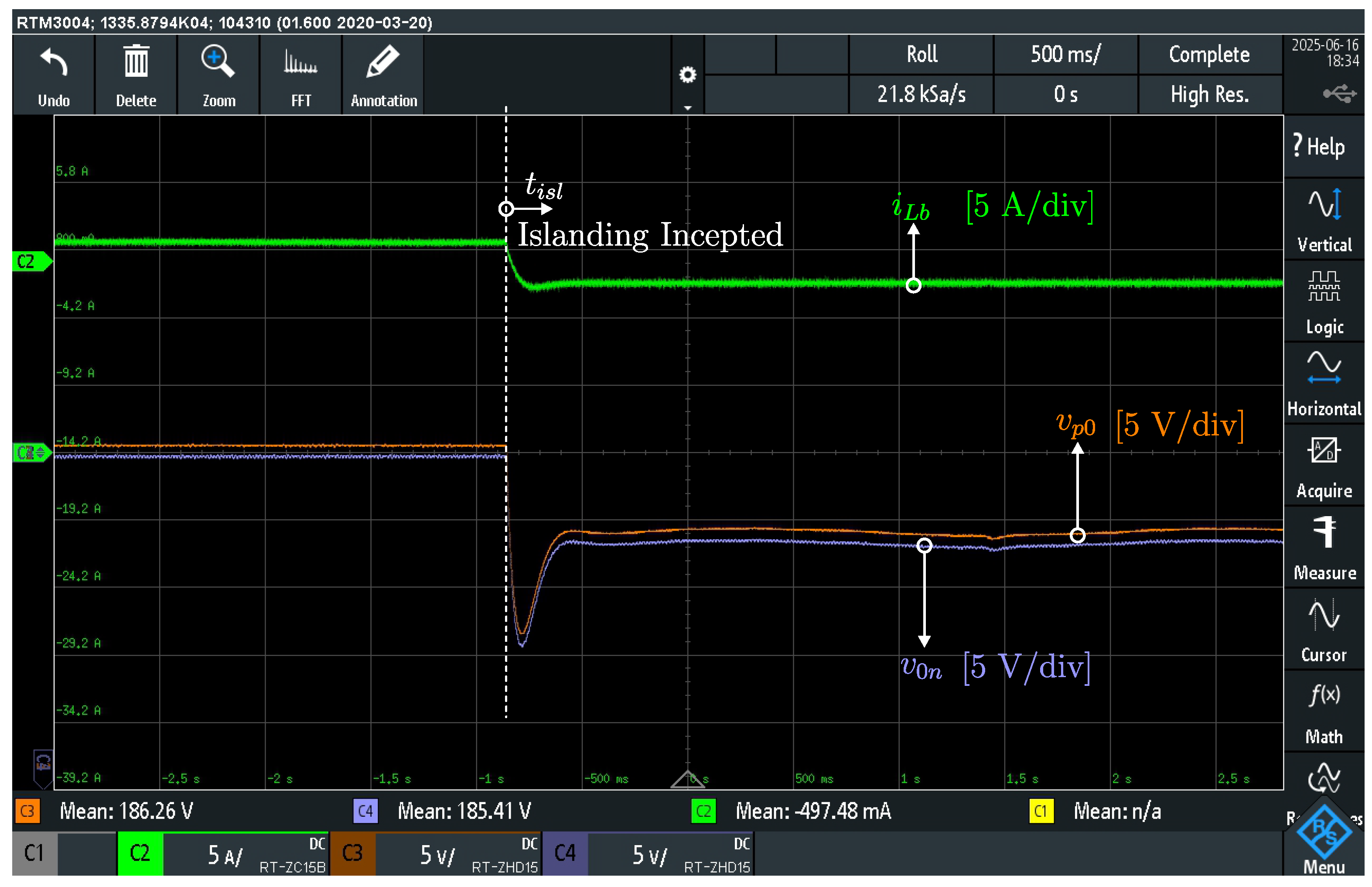
Figure 21 illustrates the transient response of the bipolar dc microgrid at the instant t i s l , when the unplanned islanding occurs. Channel 2 presents the voltage balancer current i L b (green trace, 2 A/div), Channel 3 presents the bus voltage v p 0 (orange trace, 5 V/div, offset: 190 V), and Channel 4 presents the bus voltage v 0 n (light blue trace, 5 V/div, offset: 190 V).
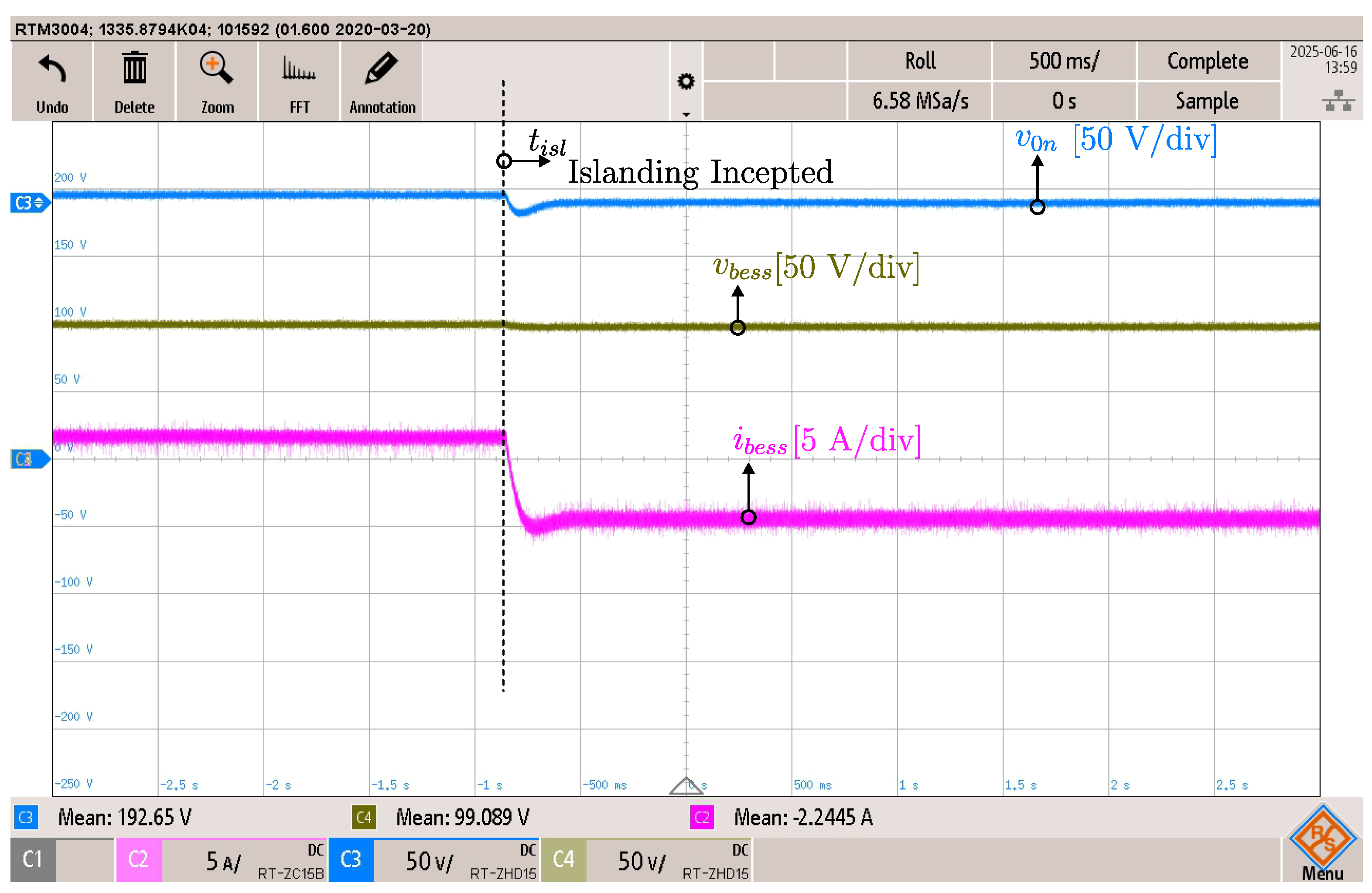
Figure 22 illustrates the transient response of the BESS converter during the unplanned islanding event at t i s l . Channel 2 presents the inductor current i b e s s (pink trace, 5 A/div), Channel 3 presents the bus voltage v 0 n (light blue trace, 2 V/div, offset: 190 V), and Channel 4 presents the output voltage v b e s s (green trace, 2 V/div, offset: 95 V).
Before t i s l , the bidirectional dc power supply regulates the total dc bus at 380 V. The voltage balancer operates in closed-loop, ensuring the balance of the intermediary voltage of the bipolar bus, and the BESS converter is connected to the 0–n dc bus, recharging the battery with approximately 1.5 A. The voltage deviation of the system is 0.8 V ( Δ U V = 0.42 % ).
At t i s l , the unplanned islanded scenario occurs when the switch S μ G opens. The bidirectional power supply is detached from the microgrid, and the BESS converter acts as the dc grid-forming converter. At this moment, the loads from the two unipolar buses are fed the BESS connected in the negative bus. The BESS provides 5 A resulting in a voltage drop of 5 V due to K d r o o p = 1 V/A. The resulting voltage is 185 V.
In the islanded scenario, the BESS feeds directly only the negative pole, but the voltage balancer doubles the voltage sourced, redirecting power from the negative pole to the positive pole, and keeping v p 0 at 184 V. This voltage deviates approximately 0.8 V from the voltage sourced in the negative pole, corresponding to Δ U V = 0.42 % . The total dc voltage v p n remains near 369 V.
The BESS current increases steadily from 0 A to 5 A, supplying the load power requirement of the microgrid. For the BESS converter, this islanding scenario is perceived as a load step. These results confirm the seamless and well-controlled transition from grid-connected operation to the islanded scenario.
Furthermore, Table 9 presents a comparison of voltages and the unbalance deviation before the islanding and after the transition to mode B.

6.7. Overview of Qualitative Experimental Tests

In Section 6.1, the voltage balancer enters in operation in open-loop. It improves the microgrid’s voltage regulation in the connected scenario. However, in Section 6.2, when subjected to more unbalanced loads, the voltage balancer becomes less effective, requiring closed-loop regulation.
In a closed-loop, it can accurately regulate the voltage on the bipolar bus, as shown in Section 6.3. The voltage balancer and the microgrid remain stable when operating with electronic loads in open-loop or in closed-loop, as in Section 6.4 and Section 6.5. In all of these cases, the voltage balancer accuracy increases when operating in closed-loop.
Finally, Section 6.6 shows the microgrid operating with the BESS, which sources power to one of the poles, and the voltage balancer, which redistributes the power to the other pole, and keeps the voltages equalized. Thus, the voltage balancer allows the bipolar microgrid to operate with a unipolar power source while balancing the unipolar voltages.
7. Conclusions

This paper experimentally validates a voltage balancing converter operating in a bipolar dc microgrid comprising a BESS converter, a bidirectional dc power supply, a buck converter, a load converter, resistive loads, and a PV converter. Because unbalanced voltages are undesired, the voltage balancer maintains the voltages v p 0 and v 0 n balanced during microgrid operation, regardless of whether resistive or constant-power loads are connected or disconnected. Experimental data confirmed the voltage balancing of unipolar voltages in unbalanced load scenarios. Furthermore, the voltage balancer is also tested in an islanding scenario experiment. After the disconnection of the dc power supply forming the dc bus, the unipolar BESS converter that operates in droop mode perceived the disconnection as a load step, and maintained the microgrid operating through a smooth transition. During this seamless transition from grid-connected to islanded operation, the voltage balancer redirected power from the unipolar BESS converter, keeping the bipolar bus operational even when only one unipolar voltage source was present. The voltage balancer equalized the unipolar voltages within a margin of less than 0.5% of the total dc voltage for unbalanced and islanded conditions.
Future work will focus on implementing hierarchical control in bipolar DC microgrids, expanding beyond the voltage balancer. The integration of a secondary control layer is expected to enhance voltage regulation and operational stability, while a tertiary control layer can enable optimal energy management.

Author Contributions

M.P.D.: Conceptualization, methodology, software, experimental validation, formal analysis, investigation, data curation, writing—original draft preparation, visualization. D.P.D.: Conceptualization, methodology, software, experimental validation, formal analysis, investigation, data curation, writing—review and editing, visualization. E.D.Q.: Software, formal analysis, investigation, data curation, writing—review and editing, visualization. K.P.d.S.: Software, formal analysis, investigation, data curation, writing—review and editing, visualization. J.C.U.P.: Conceptualization, methodology, software, experimental validation, formal analysis, investigation, data curation, writing—review and editing, visualization, supervision, project administration. J.A.P.: Methodology, software, experimental validation, formal analysis, investigation, data curation, writing—review and editing, visualization, supervision, project administration, funding acquisition. All authors have read and agreed to the published version of the manuscript.

Funding

This work was funded by Centro Paulista de Estudos da Transição Energética (CPTEn) under the grant #2021/11380-5, by the São Paulo Research Foundation (FAPESP) under grants 2016/08645-9, 2017/11623-0 and 2018/21436-5, by the National Council for Scientific and Technological Development (CNPq) under grants #200990/2022-5, #303859/2020-2 and #401216/2016-0, financed in part by the Coordenação de Aperfeiçoamento de Pessoal de Nivel Superior—Brasil (CAPES)—Finance Code 001 and it was developed under the Electricity Sector Research and Development Program PD-00063-3058/2019-PA3058: “MERGE-Microgrids for Efficient, Reliable and Greener Energy”, regulated by the National Electricity Agency (ANEEL), in partnership with CPFL Energia (Local Electricity Distributor).

Data Availability Statement

The original contributions presented in this study are included in this article. Further inquiries can be directed to the corresponding author.

Conflicts of Interest

Author Kristian P. dos Santos was employed by Federal Institute of Education, Science and Technology of Piauí. The remaining authors declare that the research was conducted in the absence of any commercial or financial relationships that could be construed as a potential conflict of interest.

References

  1. IEC. Electricity 2025—Analysis and Forecast to 2027. Briefing Paper, 2025. Available online: https://iea.blob.core.windows.net/assets/0f028d5f-26b1-47ca-ad2a-5ca3103d070a/Electricity2025.pdf (accessed on 20 August 2025).
  2. EPE. Brazilian Energy Balance 2024. Available online: https://www.epe.gov.br/sites-en/publicacoes-dados-abertos/publicacoes/PublishingImages/Paginas/Forms/Publicaes/Summary%20Report%202024.pdf (accessed on 10 August 2025).
  3. Somchit, S.; Kaewdornhan, N.; Chatthaworn, R. Enhanced Transmission Expansion Planning with a High Confidence Strategy Considering Fluctuations in Solar PV Generation and Electricity Demand. IEEE Access 2025, 13, 53100–53115. [Google Scholar] [CrossRef]
  4. da Silva, N.R. Demanda de Energica Elétrica Residencial no Brasil Segundo os Quantis de Consumo. Master’s Thesis, Universidade Federal de Viçosa, Viçosa, Brazil, 2013. [Google Scholar]
  5. Gao, Y.; Cen, Y.; Huang, M.; Zeng, J.; Chen, R.; Zhang, C. An Overview in DC Distribution System of Smart Building. In Proceedings of the 2021 International Conference on Power System Technology (POWERCON), Haikou, China, 8–9 December 2021; pp. 834–843. [Google Scholar] [CrossRef]
  6. Cai, W.; Liu, B.; Duan, S.; Jiang, L. An Active Low-Frequency Ripple Control Method Based on the Virtual Capacitor Concept for BIPV Systems. IEEE Trans. Power Electron. 2014, 29, 1733–1745. [Google Scholar] [CrossRef]
  7. Liu, B.; Duan, S.; Cai, T. Photovoltaic DC-Building-Module-Based BIPV System—Concept and Design Considerations. IEEE Trans. Power Electron. 2011, 26, 1418–1429. [Google Scholar] [CrossRef]
  8. Liu, X.; Jiang, Y.; Zhang, T.; Hao, B. Photovoltaics and Energy Storage Integrated Flexible Direct Current Distribution Systems of Buildings: Definition, Technology Review, and Application. CSEE J. Power Energy Syst. 2023, 9, 829–845. [Google Scholar] [CrossRef]
  9. Koh, L.; Soe, N.P.; Ong, H.; Zhang, Z.; Wang, J. DC renewable connected building grid for intelligent LED lighting system. In Proceedings of the 2017 IEEE 26th International Symposium on Industrial Electronics (ISIE), Edinburgh, UK, 19–21 June 2017; pp. 970–974. [Google Scholar] [CrossRef]
  10. Chinnathambi, N.; Nagappan, K.; Raja, C.; Tamilarasu, K. Internet of things-based smart residential building energy management system for a grid-connected solar photovoltaic-powered DC residential building. Int. J. Energy Res. 2021, 46, 1497–1517. [Google Scholar] [CrossRef]
  11. Aazami, R.; Moradi, M.; Shirkhani, M.; Harrison, A.; Al-Gahtani, S.F.; Elbarbary, Z.M.S. Technical Analysis of Comfort and Energy Consumption in Smart Buildings with Three Levels of Automation: Scheduling, Smart Sensors, and IoT. IEEE Access 2025, 13, 8310–8326. [Google Scholar] [CrossRef]
  12. Kleftakis, V.; Lagos, D.; Papadimitriou, C.; Hatziargyriou, N.D. Seamless Transition Between Interconnected and Islanded Operation of DC Microgrids. IEEE Trans. Smart Grid 2019, 10, 248–256. [Google Scholar] [CrossRef]
  13. PD-IEC-TR-63282:2024; LVDC Systems—Assessment of Standard Voltages and Power Quality Requirements. International Electrotechnical Commission: Geneva, Switzerland, 2024.
  14. Dragičević, T.; Lu, X.; Vasquez, J.C.; Guerrero, J.M. DC Microgrids—Part II: A Review of Power Architectures, Applications, and Standardization Issues. IEEE Trans. Power Electron. 2016, 31, 3528–3549. [Google Scholar] [CrossRef]
  15. Pompodakis, E.E.; Kryonidis, G.C.; Demoulias, C.; Alexiadis, M.C. A Generic Power Flow Algorithm for Unbalanced Islanded Hybrid AC/DC Microgrids. IEEE Trans. Power Syst. 2021, 36, 1107–1120. [Google Scholar] [CrossRef]
  16. Carvalho, E.L.; Blinov, A.; Chub, A.; Emiliani, P.; de Carne, G.; Vinnikov, D. Grid Integration of DC Buildings: Standards, Requirements and Power Converter Topologies. IEEE Open J. Power Electron. 2022, 3, 798–823. [Google Scholar] [CrossRef]
  17. Dogra, R.; Rajpurohit, B.S.; Reddy Tummuru, N. Islanding detection technique for multi-port grid-integrated DC microgrid based on superimposed components. In Proceedings of the 2020 IEEE International Power and Renewable Energy Conference, Karunagappally, India, 30 October–1 November 2020; pp. 1–6. [Google Scholar] [CrossRef]
  18. Saxena, A.; Sharma, N.K.; Samantaray, S.R. An Enhanced Differential Protection Scheme for LVDC Microgrid. IEEE J. Emerg. Sel. Top. Power Electron. 2022, 10, 2114–2125. [Google Scholar] [CrossRef]
  19. Damasceno, D.P.; Dias, M.P.; Ota, J.I.Y.; Pomilio, J.A. A Passive Islanding Detection Scheme for a Bipolar DC Microgrid. In Proceedings of the 2022 IEEE 7th Southern Power Electronics Conference (SPEC), Nadi, Fiji, 5–8 December 2022; pp. 1–6. [Google Scholar] [CrossRef]
  20. Dias, M.P.; Damasceno, D.P.; Peña, J.C.U.; Ota, J.I.Y.; Pomilio, J.A. Bipolar DC Microgrid with Voltage Balancer: System Modelling and Hardware-in-the-loop Simulation. In Proceedings of the 2023 IEEE 8th Southern Power Electronics Conference and 17th Brazilian Power Electronics Conference (SPEC/COBEP), Florianopolis, Brazil, 26–29 November 2023; pp. 1–6. [Google Scholar] [CrossRef]
  21. Dias, M.P.; Ota, J.I.Y.; Pomilio, J.A. DC Current Redistributor for Compensating Unbalanced Loads and Interfacing Energy Storage Systems in More Electrical Aircraft. In Proceedings of the 2021 IEEE Southern Power Electronics Conference (SPEC), Kigali, Rwanda, 6–9 December 2021; pp. 1–6. [Google Scholar] [CrossRef]
  22. Dias, M.P.; Guillardi, H.; Guerreiro, J.F.; Ota, J.I.Y.; Pomilio, J.A.; Mattavelli, P. DC Current Redistributor for Electric Aircraft System. In Proceedings of the 2019 IEEE 15th Brazilian Power Electronics Conference and 5th IEEE Southern Power Electronics Conference (COBEP/SPEC), Santos, Brazil, 1–4 December 2019; pp. 1–6. [Google Scholar] [CrossRef]
  23. Bueno, A.G. Three-Phase Four-Wire PWM Boost Rectifier. Master’s Thesis, School of Electrical and Computer Engineering of the University of Campinas, São Paulo, Brazil, 2018. (In portuguese). [Google Scholar]
  24. Kim, S.H.; Byun, H.J.; Jeong, W.S.; Yi, J.; Won, C.Y. Hierarchical Control with Voltage Balancing and Energy Management for Bipolar DC Microgrid. IEEE Trans. Ind. Electron. 2023, 70, 9147–9157. [Google Scholar] [CrossRef]
  25. Li, X.; Guo, L.; Guo, Z.; Wang, C.; Hong, C.; Zhang, Y.; Yang, J.; Li, Y. Coordinated control of multiple voltage balancers in a Bipolar DC microgrid. In Proceedings of the 2017 IEEE Power & Energy Society General Meeting, Chicago, IL, USA, 16–20 July 2017; pp. 1–5. [Google Scholar] [CrossRef]
  26. Lee, J.Y.; Cho, Y.P.; Jung, J.H. Single-Stage Voltage Balancer with High-Frequency Isolation for Bipolar LVDC Distribution System. IEEE Trans. Ind. Electron. 2020, 67, 3596–3606. [Google Scholar] [CrossRef]
  27. Shah, F.M.; Maqsood, S.; Shah, Z.M.; Muhammad, F.; Kim, S. Multilevel LVDC Distribution System with Voltage Unbalancing and Disturbance Rejection Control Topology. IEEE Access 2020, 8, 133787–133801. [Google Scholar] [CrossRef]
  28. Prabhakaran, P.; Agarwal, V. Novel Boost-SEPIC Type Interleaved DC–DC Converter for Mitigation of Voltage Imbalance in a Low-Voltage Bipolar DC Microgrid. IEEE Trans. Ind. Electron. 2020, 67, 6494–6504. [Google Scholar] [CrossRef]
  29. Lago, J.; Moia, J.; Heldwein, M.L. Evaluation of power converters to implement bipolar DC active distribution networks—DC-DC converters. In Proceedings of the 2011 IEEE Energy Conversion Congress and Exposition, Phoenix, AZ, USA, 17–22 September 2011; pp. 985–990. [Google Scholar] [CrossRef]
  30. Zhang, X.; Guo, C.; Zhou, Y.; Xu, X.; Liao, J.; Zhou, N.; Wang, Q. Unbalanced Voltage Suppression of Bipolar DC Microgrids with Integration of DC Zero-Carbon Buildings. J. Mod. Power Syst. Clean Energy 2024, 12, 1942–1956. [Google Scholar] [CrossRef]
  31. Han, H.; Zheng, X.; Su, M.; Sun, Y.; Liu, Z.; Liu, H.; Ling, T.; Liu, X. A Fast Fault Diagnosis Scheme for Ring Bus DC Microgrids With Fewer Sensors. IEEE Trans. Power Deliv. 2024, 39, 283–295. [Google Scholar] [CrossRef]
  32. Mudaliyar, S.; Mishra, S. Coordinated Voltage Control of a Grid Connected Ring DC Microgrid with Energy Hub. IEEE Trans. Smart Grid 2019, 10, 1939–1948. [Google Scholar] [CrossRef]
  33. Li, X.; Guo, L.; Zhang, S.; Wang, C.; Li, Y.W.; Chen, A.; Feng, Y. Observer-Based DC Voltage Droop and Current Feed-Forward Control of a DC Microgrid. IEEE Trans. Smart Grid 2018, 9, 5207–5216. [Google Scholar] [CrossRef]
  34. Erickson, R.; Maksimovic, D. Fundamentals of Power Electronics; Springer: Cham, Switzerland, 2020. [Google Scholar] [CrossRef]
  35. Corradini, L.; Maksimović, D.; Mattavelli, P.; Zane, R. Digital Control of High-Frequency Switched-Mode Power Converters; John Wiley & Sons: Hoboken, NJ, USA, 2015. [Google Scholar]
  36. Liu, G. Advanced Controllers of Power Electronic Converters in DC Microgrids. Ph.D. Thesis, Scuola di Dottorato di Ricerca in Ingegneria Meccatronica e Dell’Innovazione Meccanica del Prodotto, Universita degli Studi di Padova, Padova, Italy, 2019. [Google Scholar]
Figure 1. Single-line bipolar dc microgrid with ESS connected to the bus.
Processes 13 03734 g001
Figure 2. Bipolar dc microgrid equivalent representation.
Processes 13 03734 g002
Figure 3. Distribution of voltage balancers in bipolar dc microgrid (a) Centralized voltage balancers (b) Distributed voltage balancers.
Processes 13 03734 g003
Figure 4. Several architectures of voltage balancers. (a) Voltage balancer with merged ESS. (b) DAB based voltage balancer. (c) Bipolar CF-DAB Voltage balancer.
Processes 13 03734 g004
Figure 5. Ring Bipolar dc microgrid.
Processes 13 03734 g005
Figure 6. Bipolar dc bus microgrid.
Processes 13 03734 g006
Figure 7. Control block of the bipolar dc microgrid. (a) Control block diagram of the buck converter. (b) Control block diagram of the BESS converter. (c) Control block diagram of the voltage balancer.
Processes 13 03734 g007
Figure 8. Bipolar dc microgrid experimental prototype.
Processes 13 03734 g008
Figure 9. Equivalent experimental setup of the bipolar dc microgrid.
Processes 13 03734 g009
Figure 10. BESS converter, buck converter and the control board.
Processes 13 03734 g010
Figure 11. Control board and the voltage Balancing converter.
Processes 13 03734 g011
Figure 12. Experimental setup of the voltage balancer analysis.
Processes 13 03734 g012
Figure 13. Bipolar dc microgrid results with the voltage balancer. CH2 (green trace): voltage balancer current i L b , CH3 (orange trace): 190 V voltage v p 0 with an offset: 190 V, CH4 (light blue trace): 190 V voltage v 0 n with an offset: 190 V.
Processes 13 03734 g013
Figure 14. Bipolar dc microgrid results with a resistive load step. CH1 (yellow trace): load current i R 100 Ω , CH2 (green trace): voltage balancer current i L b , CH3 (orange trace): 190 V voltage v p 0 with an offset: 190 V, CH4 (light blue trace): 190 V voltage v 0 n with an offset: 190 V.
Processes 13 03734 g014
Figure 15. Voltage balancer in closed-loop: Bipolar dc microgrid results with a resistive load step. CH1 (yellow trace): load current i R 100 Ω , CH2 (green trace): voltage balancer current i L b , CH3 (orange trace): 190 V voltage v p 0 with an offset: 190 V, CH4 (light blue trace): 190 V voltage v 0 n with an offset: 190 V.
Processes 13 03734 g015
Figure 16. Experimental setup of the 48 V load converter.
Processes 13 03734 g016
Figure 17. Bipolar dc microgrid results with the connection of the load converter. CH1 (yellow trace): load current i R M W 48 , CH2 (green trace): voltage balancer current i L b , CH3 (orange trace): 190 V voltage v p 0 , offset: 190 V, CH4 (light blue trace): 190 V voltage v 0 n , offset: 190 V.
Processes 13 03734 g017
Figure 18. Bipolar dc microgrid results with the disconnection of the load converter. CH1 (yellow trace): load current i R M W 48 , CH2 (green trace): voltage balancer current i L b , CH3 (orange trace): 190 V voltage v p 0 , offset: 190 V, CH4 (light blue trace): 190 V voltage v 0 n ; offset: 190 V.
Processes 13 03734 g018
Figure 19. Voltage balancer in closed-loop: Bipolar dc microgrid results with the connection of the load converter. CH1 (yellow trace): load current i R M W 48 , CH2 (green trace): voltage balancer current i L b , CH3 (orange trace): 190 V voltage v p 0 , offset: 190 V, CH4 (light blue trace): 190 V voltage v 0 n , offset: 190 V.
Processes 13 03734 g019
Figure 20. Voltage balancer in closed-loop: Bipolar dc microgrid results with the disconnection of the load converter. CH1 (yellow trace): load current i R M W 48 , CH2 (green trace): voltage balancer current i L b , CH3 (orange trace): 190 V voltage v p 0 , offset: 190 V, CH4 (light blue trace): 190 V voltage v 0 n ; offset: 190 V.
Processes 13 03734 g020
Figure 21. Bipolar dc microgrid in seamless disconnection of the dc grid former. CH2 (green trace): voltage balancer current i L b , CH3 (orange trace): 190 V voltage v p 0 with an offset: 190 V, CH4 (light blue trace): 190 V voltage v 0 n with an offset: 190 V.
Processes 13 03734 g021
Figure 22. Dynamic behavior of the BESS converter in a seamless disconnection of the dc grid former.CH2 (pink): Bess inductor current i b e s s , CH3 (light blue): 190 V voltage v 0 n with an offset: 190 V, CH4 (green): Bess voltage v b e s s , with an offset: 95 V.
Processes 13 03734 g022
Table 1. BESS and Buck control parameters.
ParametersValue
Buck Phase Margin M F = 75.5 °
Buck Cutoff frequency f c = 535  Hz
Buck pole frequency (Hz) f p = 5.729432506466 × 10 4
Buck pole frequency (rad/s) ω p 2 = 8.999771535776 × 10 4
Buck zero frequency (rad/s) ω z = 27.416263740294
Buck proportional gain k P D = 1.584761914572 × 10 4
Buck integral frequency (rad/s) ω L = 1.570796326794 × 10 3
BESS proportional current gain ( K p c B E S S )0.0794
BESS integral current gain ( K i c B E S S )59.8909
BESS proportional voltage gain ( K p v B E S S )0.33
BESS integral voltage gain ( K i v B E S S )24.8806
Table 2. v 0 and i b e s s Voltage and current gain of the control board.
ParametersValue
CH0 Maximum input voltage ( v C H 0 m a x )109.53 V/−109.53 V
HCPL input gain ( K d i v )1825.928 u
Offset CH0 Channel ( o f f s e t C H 0 )1.478 V
Anti-aliasing gain ( K A A C H 0 )1
ADC input voltage ( v a d c v )2.478 V
Maximum input current ( i L m a x )+/−10 A rms/14.14 A pico
Offset CH2 Channel ( o f f s e t C H 2 )1.477 V
Anti-aliasing gain ( K A A i )0.18
ADC input voltage ( v a d c v )2.477 V
Table 3. v p 0 and v 0 n Voltage gain in the control board.
ParametersValue
CH6 and CH7 Maximum voltage ( v i m a x )109.53 V/−109.53 V
CH6 and CH7 HCPL input gain ( K d i v )1825.928 u
Offset CH6 Channel ( o f f s e t C H 6 )1.478 V
Offset CH7 Channel ( o f f s e t C H 7 )1.479 V
CH6 and CH7 Anti-aliasing gain ( K A A v )1
CH6 ADC input voltage ( v a d c C H 6 )2.478 V
CH7 ADC input voltage ( v a d c C H 7 )2.479 V
Table 4. Microgrid and voltage balancer parameters.
ParametersValue
Bipolar dc microgrid power ( P μ G )3 kW
BESS rated power ( P b e s s )1 kW
Total dc bus voltage ( v p n )380 V
Intermediary voltages ( v 0 n = v p 0 )190 V
Voltage Balancer inductor ( L b )1.875 mH
Voltage Balancer capacitor bank ( C i v b )1360 μF
Bipolar bus capacitors ( C 1 = C 2 )470 μF
voltage balancer switching frequency ( f s b = f s v b )20 kHz
Table 5. BESS converter and Buck parameters.
ParametersValue
BESS Low side inductor ( L l v )2 mH
BESS High side inductor ( L h v )none
BESS Low side capacitor ( C l v )220 μF
BESS High side capacitor ( C h v )940 μF
BESS Battery bank voltage ( v l v )95 V
Damping branch capacitors ( C d b = C d )none
Damping branch resistances ( R d b = R d )none
Buck output power ( P b u c k )950 W
Buck converter output voltage ( V o )95 V
Buck converter inductance2 mH
Buck converter low side capacitor ( C o )220 μF
Buck converter high side capacitor ( C f )940 μF
BESS and buck switching frequency ( f s b = f s v b )20 kHz
Table 6. PV converter parameters.
ParametersValue
PV panel voltage ( v p v )220 V
PV power ( P p v )2 kW
PV inductor ( L p v )700 μH
PV input capacitor ( C p v )2000 μF
PV Output capacitor ( C o 2 )4700 μF
Table 7. Comparison of experimental results with resistive loads.
Load ResistanceIntermediary Bus Voltages Δ UV Δ UV (%)
R 1 = 88 Ω and R 2 = 150 Ω (before t e at open-loop mode) v 0 n = 210 V and v p 0 = 170 V40 V 21 %
R 1 = 88 Ω and R 2 = 150 Ω (after t e at open-loop mode) v 0 n = 188.5  V and v p 0 = 191.5  V3 V 1.66 %
R 1 = 88 Ω , R 2 = 150 Ω , and  R 3 = 100 Ω (after t r at open-loop mode) v 0 n = 184 V and v p 0 = 196 V12 V 6.3 %
R 1 = 176 Ω and R 2 = 150 Ω (before t r at closed-loop mode) v 0 n = 189.75  V and v p 0 = 190.25  V 0.5  V 0.26 %
R 1 = 176 Ω , R 2 = 150 Ω and R 3 = 100 Ω (after t r at closed-loop mode) v 0 n = 189.75  V and v p 0 = 190.25  V 0.5  V 0.26 %
Table 8. Comparison of experimental results with electronic loads.
Load ResistenceIntermediary Bus Voltages Δ UV Δ UV (%)
R 1 = 176 Ω and R 2 = 150 Ω (before t w at open-loop mode) v 0 n = 188.5  V and v p 0 = 191.5  V3 V 1.6 %
R 1 = 176 Ω and R 2 = 150 Ω (after t w at open-loop mode) v 0 n = 184 V and v p 0 = 196 V12 V 6.3 %
R 1 = 176 Ω and R 2 = 150 Ω (before t z at closed-loop mode) v 0 n = 189.6  V and v p 0 = 190.4  V 0.8  V 0.42 %
R 1 = 176 Ω and R 2 = 150 Ω (after t z at closed-loop mode) v 0 n = 189.6  V and v p 0 = 190.4  V 0.8  V 0.42 %
Table 9. Overview of the experimental results.
Load ResistenceIntermediary Bus Voltages Δ UV Δ UV (%)
R 1 = 176 Ω and R 2 = 150 Ω (before t i s l ) v 0 n = 189.6  V and v p 0 = 190.4  V 0.8  V 0.42 %
R 1 = 176 Ω and R 2 = 150 Ω (after t i s l ) v 0 n = 184.6  V and v p 0 = 183.8  V 0.8  V 0.42 %
Disclaimer/Publisher’s Note: The statements, opinions and data contained in all publications are solely those of the individual author(s) and contributor(s) and not of MDPI and/or the editor(s). MDPI and/or the editor(s) disclaim responsibility for any injury to people or property resulting from any ideas, methods, instructions or products referred to in the content.