Review

Foundry Service of CMOS MEMS Processes and the Case Study of the Flow Sensor

1
Department of Mechanical and Electro-Mechanical Engineering, Tamkang University, New Taipei City 251301, Taiwan
2
Department of Electrical and Electronics Engineering, Tamkang University, New Taipei City 251301, Taiwan
3
Department of Mechanical and Aerospace Engineering, The Hong Kong University of Science and Technology, Clear Water Bay, Kowloon, Hong Kong 999077, China
*
Author to whom correspondence should be addressed.
Processes 2022, 10(7), 1280; https://doi.org/10.3390/pr10071280
Submission received: 26 April 2022 / Revised: 3 June 2022 / Accepted: 28 June 2022 / Published: 29 June 2022

Abstract

:
The complementary metal-oxide-semiconductor (CMOS) process is the main stream to fabricate integrated circuits (ICs) in the semiconductor industry. Microelectromechanical systems (MEMS), when combined with CMOS electronics to form the CMOS MEMS process, have the merits of small features, low power consumption, on-chip circuitry, and high sensitivity to develop microsensors and micro actuators. Firstly, the authors review the educational CMOS MEMS foundry service provided by the Taiwan Semiconductor Research Institute (TSRI) allied with the United Microelectronics Corporation (UMC) and the Taiwan Semiconductor Manufacturing Company (TSMC). Taiwan’s foundry service of ICs is leading in the world. Secondly, the authors show the new flow sensor integrated with an instrumentation amplifier (IA) fabricated by the latest UMC 0.18 µm CMOS MEMS process as the case study. The new flow sensor adopted the self-heating resistive-thermal-detector (RTD) to sense the flow speed. This self-heating RTD half-bridge alone gives a normalized output sensitivity of 138 µV/V/(m/s)/mW only. After being integrated with an on-chip amplifier gain of 20 dB, the overall sensitivity of the flow sensor was measured and substantially improved to 1388 µV/V/(m/s)/mW for the flow speed range of 0–5 m/s. Finally, the advantages of the CMOS MEMS flow sensors are justified and discussed by the testing results.

1. Introduction

When humans entered the 21st century from the 20th century, the cross-sector integration of science and technology was constantly emerging, in conjunction with the trend of miniaturization, multi-functionality, and precision. It is the development of various cutting-edge technologies and industries (including nanotechnology, materials, chemicals, electronics, computers, information, photovoltaics, machinery, medicine, biotechnology, health care, environmental protection, and energy, etc.), and will have a huge impact on human life, even economic and wealth distribution. The first to propose the concept of microelectromechanical systems (MEMS) or micro system technology (MST) was the physicist, R. Feynman [1]. In 1959, at the annual meeting of the American Physical Society, he delivered a speech entitled “There is plenty of room at the bottom” to attract people’s attention to small-scale science and technology. Shortly after Feynman’s second speech “Infinitesimal machinery”, this emerging technology measured in units of the “micrometer” (μm). The invention of the transistor at Bell Telephone Laboratories in 1947 sparked a fast-growing microelectronic technology [2,3]. Piezoresistive silicon strain gauges were introduced in the late 1950s by Kulite Semiconductor, with Bell Lab’s first licensee of patents on semiconductor piezoresistance reported in 1954 [4,5]. It was discovered that the piezoresistive effect in Ge and Si had the potential to produce Ge and Si strain gauges with a gauge factor (i.e., instrument sensitivity) 10 to 20 times greater than those based on metal films [4]. As a result, Si strain gauges began to be developed commercially in 1958. The first high-volume pressure sensor was marketed by National Semiconductor in 1974. This sensor included a temperature controller for constant-temperature operation. In 1982, silicon was called a mechanical material in K. Petersen’s famous review article [6]. During 1987–1988, a turning point was reached in micromachining when, for the first time, techniques for the integrated fabrication of mechanisms (i.e., rigid bodies connected by joints for transmitting, controlling, or constraining relative movement) on Si were demonstrated. The resonant gate transistor (RGT) [7] was dissimilar with conventional transistors in that it was not fixed to the gate oxide. As an alternative, it was movable and cantilevered with respect to the substrate used. In 1967, the RGT was the earliest demonstration of micro electrostatic actuators. It was also the first demonstration of surface micromachining techniques. In 1971, Intel publicly introduced the world’s first single chip microprocessor, the Intel 4004. The 4004 powered the Busicom calculator and was Intel’s first microprocessor [8]. Muller, Fan, and Tai invented the world’s first micrometer-sized electrostatic motor (micromotor) in 1989 at the University of California, Berkeley, using the IC process technology before the official terminology of MEMS [9,10]. R. S. Muller of UC Berkeley started the IEEE Electron Devices Society of IEEE/ASME Journal of Microelectromechanical Systems in 1990. The story of the invention of the charge-coupled device (CCD) is easier to unravel: L.F.J. Sangster [11] of Philips Research Laboratory and W.S. Boyle and G.E. Smith [12] of Bell Laboratories at Murray Hill independently came up with the CCD structure. In the United States, J.B Angell, Stanford University [13,14,15], and K. D. Wise from University of Michigan also made astonishing steps with their work [13,15,16,17,18,19]. Though there were many initiatives in the 1960s, it is almost certain that Stanford University’s Integrated Circuits Laboratory, under the guidance of Prof. J. Angell, can be credited with being the renowned research group to be active in the field of silicon sensors and micromachining. Another enthusiastic group had also been working on silicon sensors for biomedical applications under the guidance of sensor pioneer Prof. W. H Ko, Case Western Reserve University [20,21]. The first of the gate-controlled diode designed by Zemel et al. [22] at the University of Pennsylvania can also be noted. In Sweden, I. Lundstrom et al. invented Pd-gate, which led many to interesting gas-sensitive devices at the University of Linkoping in 1975 [23], and G. Stemme, who worked at Royal Institute of Technology, Sweden, also made contributions in this field [24]. The first to point out the necessity of applying CAD to sensors was S. D Senturia from MIT, UK, in 1976 [25]. The first silicon flow sensor based on the temperature sensitivity of a diffused Wheatstone bridge in silicon was designed by van Putten and Middelhoek Delf University of Technology in 1974 [26]. P. Bergveld of the University of Twente [27] and R Puers of K. U Leuven are also remarkable mentions from the Netherlands [28]. The Institute of Integrated Micro and Nano Systems, School of Engineering and Electronics, Scottish Microelectronics Centre, University of Edinburgh, Scotland; T. Matsuo of Tokohu University, Japan [17]; M. Bao of Fudan University, China [20]; W. Gopel from the University of Tubigen,1983 [29,30,31]; and E. Obermeier T.U Berlin, Germany 1987 [32,33] are some of the renowned institutions and professors from distinguished universities from several countries whose era should be remembered.
In 1994, Cornell University introduced a bulk micromachining process called single crystal reactive etching and metallization (SCREAM) [34]. Special mention is also made of Petersen’s review paper [6], a truly seminal work that gave the field a much-needed impetus. From 2005 to 2021 with the advancement in MEMS fabrication, manufacturing technologies and processes, the various applications of MEMS structures were explored and developed, some of which are airbag accelerometers, intelligent tires, vehicle security systems, inertial brake lights, headlight leveling, rollover detection; inkjet printer heads, projection screen and televisions, mass data storage systems, sports training devices, earthquake detection and gas shutoff, projection displays in portable communications devices and instrumentation, voltage controlled oscillators (VCOs); surveillance, arming systems, embedded sensors, data storage, aircraft control, tanks control; and blood pressure sensors, muscle stimulators and drug delivery systems, implanted pressure sensors, prosthetics body parts, polymerase chain reaction (PCR) microsystems, micromachined scanning tunneling microscopes (STMs), biochips for detection of hazardous chemical and biological agents, high-throughput drug screening, and so on.
Thus, we can observe, from the last several decades, that there has been rapid growth of complementary metal-oxide-semiconductor (CMOS) MEMS fabrication technology, which enables the manufacturing of micro devices of various sensors and actuators. The term MEMS originally meant miniaturized electromechanical actuators but now applies to a broad family of micromachined sensors, actuators, and systems with coupled electrical, mechanical, radiant, thermal, magnetic, and chemical effects. The technologies are based on the sequence of the fabrication of CMOS circuitry and MEMS elements, while silicon-on-insulator (SOI) and CMOS MEMS are discussed separately [4,35,36,37]. There are different CMOS MEMS fabrication approaches, namely pre-CMOS, intermediate-CMOS, and post-CMOS. Starting from 0.8 µm double-polysilicon–double-metal (DPDM) CMOS process, tremendous efforts have been made to continuously improve process yield and reliability, while minimal feature sizes and fabrication cost continue to decrease [35,38,39,40]. The concept of producing MEMS devices in a standard CMOS process was first described by H. Baltes [29,39,41,42,43,44,45,46,47,48]; other researchers from Switzerland, namely N. F. de Rooij, University of Neuchatel [49] and R. Popovic, EPFL [50], are famous contributors to this field. Baltes conducted the feasibility study followed by the launch of several national agencies that had the ability to provide the CMOS foundry service. The motivation for its research and development (R&D) was to directly use off-the-shelf IC foundry equipment and integrate the MEMS sensors and actuators with sensing signal processing on the same silicon chip (on-chip circuitry). Designers of MEMS devices only need to design the layout and, after the completion of the foundry service, to perform post-processing to obtain the desired MEMS devices. The benefits of the MEMS sensors, actuators, and the signal processing circuits can be linked on-chip together to reduce the influence of external noise to a minimum and improve component performance. After verifying the stability and reliability of the CMOS MEMS devices by using CMOS foundry, it may be quick to enter the production market and create business opportunities. Semiconductor roadmaps show the current state and, more important, outline the future performance of CMOS technology with ever-increasing integration density and decreasing feature size [37,51,52,53,54,55]. With the breakthrough of technologies, it has enabled integrating MEMS structures with ICs on a single CMOS substrate, so-called monolithic CMOS MEMS integration.
CMOS-compatible MEMS technologies includes bulk micromachining (wet or dry, isotropic or anisotropic, from wafer front or back), surface micromachining (sacrificial dielectric and/or metal or polysilicon), micromachining before/after completion of the IC process (pre-CMOS/post-CMOS), use of IC materials for microstructures with electro-thermo or opto-mechanical functions, thin film deposition, chemical-mechanical polishing (CMP), and wafer bonding. However, if the above cannot be exactly fabricated in the simple clean room of researchers’ laboratory, commercial CMOS foundry service could be found as help.
Caltech released the first IC-integrated flexible shear stress sensor skin in 2003, which can instantly respond to aerodynamics drag. The measurement signals are mixed for adaptive flow control and the flight control of fixed-wing micro-aircraft [56,57]. MEMS multi-sensor chip for gas flow sensing was also developed by Xu et al. [58]. The above-mentioned sensor-actuated array chips were applied to a 2 μm CMOS MEMS foundry service. Recently, the Hong Kong University of Science and Technology (HKUST) and National Chao-Tong University (NCTU) have co-developed a calorimetric flow sensor using a CMOS 0.18 μm double-poly-four-metal (2P4M) MEMS foundry service provided by the Chip Implementation Center (CIC) of Taiwan to completely manufacture the overall chip [59,60].
The authors have chosen flow sensor to be a design example later in Section 4. Some reasons why the flow sensor was selected as the case study herein are as follows:
  • Flow sensors have many emerging applications such as in oxygen respirators [61], leak detection [62], flow rate detection [59,60], gas supply control [58,63], air speed detection of wind tunnel [64], wind turbine [65,66,67,68], biomimetic flapping wing studies [69,70,71,72,73,74,75], etc. A robust and miniaturized instrument and measurement system is required to obtain accurate and reliable flow speed recordings of the above applications.
  • Compared to other mechanical sensors, fewer flow sensors were developed by the CMOS MEMS foundry service and deserve to be discussed more [76,77].
  • The design configurations of flow sensors are quite different from other mechanical sensors such as pressure sensors and inertial sensors [78]. Their requirement about the post-process was different from other MEMS sensors as well. By including this case study, one can complete the addressing of CMOS MEMS foundry technology.
It is indeed important to mention future trends, where a number of researchers have started exploring more about Silicon carbide materials and nanostructures. The study of these materials requires a good understanding of physical, biological and chemical properties, fundamental studies, as well as applied, theoretical and/or computational studies related to several new applications. Bulk silicon carbide is a wide-bandgap semiconductor with different crystalline forms owing to excellent electronic characteristics; it has mainly been used for high-temperature, high-frequency, and high-power electronic devices. It is also recognized as one of the best biocompatible materials, especially in cardiovascular and blood-contacting implants and other biomedical devices [79,80,81,82,83,84,85,86].

2. CMOS MEMS Foundry Service

United Microelectronics Corporation (UMC) was founded as Taiwan’s first IC fabrication company in 1980 as a spin-off from the government-sponsored Industrial Technology Research Institute (ITRI) in Hsinchu, Taiwan. Being a significant supplier to the automotive industry, UMC has four 300 mm fabs: one in Tainan, Taiwan; one in Singapore; one in Xiamen, China; and one in Japan. UMC also has several 200 mm fabs in Hsinchu and Suzhou, China. In 1995, the foundry service just started. In 1996, the UMC 0.35 µm CMOS process was released successfully. In 1997 and 1999, the minimum line width or the critical dimension (CD) was upgraded to 0.35 µm and 0.18 µm, respectively. At that time, UMC focused on improving their CMOS IC process capability only. The CMOS MEMS researchers need to carry out their die-level post-process of CMOS MEMS personally, e.g., by performing their own plasma-enhanced chemical vapor deposition (PECVD) process in which the deposition of thin films of various materials takes place at a low temperature (<350 °C) that the standard CMOS chips can endure. The various post-processes after the CMOS standard process may be also followed by die-level photolithography, wet etching (backside), wet etching (front side), wet etching followed by electroplating nickel, or wet etching (fronts side) followed by gelatin coating [87,88] or parylene coating [89], etc. The details will be mentioned in Section 3.
Taiwan Semiconductor Manufacturing Company, Ltd. (TSMC) is another Taiwanese multinational semiconductor contract manufacturing and design company with its headquarters and main operations located in Hsinchu Scientific Park in Taiwan. On 300 mm wafers, currently, TSMC has silicon lithography on node sizes ranging from 0.13 µm to 5 nm and is ranked the number one of the IC foundry providers in the world. The capability of the IC foundry service in Taiwan proves its top leading place in the globe. The reasons are not only due to the strong IC design houses and the reliable equipment supply of the semiconductor process but also due to the high utility rate of the process equipment and high product yield rate. For TSMC especially, they additionally created the advantage of flexibility in process sequence and process conditions and set up a very high entry barrier, which other IC fab companies may not easily surpass.
Regarding the IC designer training for students in Taiwan, the Ministry of Science and Technology (MOST; or National Science Council) founded the CIC in Hsinchu Scientific Park. CIC provided low-price or free access of Cadence software to the academics and called for IC designs from all universities in Taiwan regularly. After review and defense, CIC granted the real chip implementation for the selected IC designs and merged the selected IC layouts into a multi-project-wafer (MPW). Finally, CIC sent the photomasks to TSMC or UMC for fabricating a batch of wafers with these selected IC designs. After the IC foundry service, the IC designers could receive 20–40 pieces of CMOS IC chips for testing and verifying the functionality. The student designers had obligations to submit the test reports to CIC within months after they received the IC chips. Through this kind of education training, using real IC foundry services with several times of call-for-designs every year, CIC trained many IC student designers for IC design houses as well as developing or exploring some advanced IC circuit designs at the same time. It is important to note that, many universities do not have proper clean rooms except for a few of them. Maintaining a high-class clean room needs millions in investment. Like our research team, many other researchers are able to use this foundry service to fabricate the novel design using the CMOS MEMS process without any huge investment. The Sensor and IC designer could fabricate their design model smoothly without much hindrance, and the foundry companies also kept updated about the new design invention and innovation. Both the teams mutually benefitted from the faster development process.
The commercial IC design framework has been standardized by Cadence with Tenor (layout design), H-SPICE (circuit simulation), Verilog (IC verification), and so on. Therefore, CIC provided a huge education discount for all universities in Taiwan to buy the user license of Cadence. All student users needed to use this IC design software as the compatible design platform for doing their IC design via the CIC foundry service or even in IC technology transfer to industries. In addition, the well-trained students by CIC could easily find jobs in IC design houses after their graduation from campus. Most important of all, because CIC always asked help from TSMC and UMC about their latest version of the CMOS IC foundry service, the design rule of the minimum line width was accordingly improved from the earlier 0.35 μm CMOS process down to the 0.18 μm CMOS process.
Therefore, the IC designers in universities could access the state-of-art of IC foundry service in Taiwan and have much less time lag in developing the tiny IC chips in their current stages. CIC is not the first research center to use the MPW concept to provide the IC foundry service. The most famous prior example is the Metal Oxide Semiconductor Implementation Service (MOSIS) in the USA, with the provider MCNC (Microelectronics Center of North Carolina). As the CIC’s single-poly-three-metal (1P3M) CMOS structures show in Figure 1, the corresponding sequence of material layers with their specific thickness and doping concentration cannot be changed. The only thing the IC/MEMS designers can change is their layouts of IC/MEMS devices. Compared to MOSIS in the USA, the IC foundry service in CIC does not charge the student designers in Taiwan. However, CIC has the authority to turn down any IC design proposals.

2.1. Early Development of CMOS MEMS

The research on CMOS MEMS devices in Taiwan was started in National Taiwan University (NTU). It began with Chang, Lu, and Liu asking for help with CIC’s CMOS foundry to guide students to attend the IC design courses held in CIC in the summer of 1994 and to start the layout design of capacitive micro accelerometers, piezoresistive micro pressure sensors, and sensing signal reading circuits [37,91]. The layout designers must design IC on one side and use the software to repeatedly check, simulate, and verify to minimize the possible bugs in the other side. For this reason, the IC design software focuses on the integration of transistor components and processes with known characteristics and completes the huge IC system. The designers did not receive much stress that the micro-structured layers of the wafer were subjected to, and they were not told how to perform the conversion of physical signals into electrical signals for sensing/actuating, either [92]. In other words, if they would have liked to use commercial IC design software to design or even manufacture CMOS MEMS devices, they must have first clarified the fundamental differences between transistor IC and CMOS MEMS devices. In addition, they needed to communicate this CMOS MEMS concept to CIC leaders who originally worked on the standardization and protocol of IC foundry. Otherwise, the IC designer would be amazed about the “strange” layout design methodology of CMOS MEMS devices. For example, the CMOS MEMS designers still used the Cadence software to draw layouts, but they needed not go through the complete verification procedure of the standard IC because MEMS structures are not ICs. The exact verification of the complete ICs should include the followings: (1) design rule check (DRC): checks whether the layout patterns are too dense, and ensure the foundry’s production correctness, and there will be no short circuit problem; (2) electrical rule check (ERC): checks electrical characteristics; (3) layout versus schematic (LVS): compares and map the layout with the logic circuit of the schematic; and (4) layout parameter extraction (LPE): captures the electrical parameters of the layout.
For the MEMS device of the non-signal processing circuit, DRC verification is necessary to ensure that the microstructure can be successfully made, but the other three verifications (2–4) to MEMS sensor are not required (for example, a variable capacitor membrane subject to a pressure loading cannot be given or simulated for its capacitance change). Furthermore, for an IC designer, it seems a waste of a chip area of 400 × 400 µm2 to make a single sensor capacitor because making an 8086 microprocessor may use the similar chip area. Even though the dimensions of the MEMS device are well simulated and determined in advance by finite element analysis (FEA), which has not yet been integrated into the circuit design software so far. The MEMS engineers also need to conduct cross-domain communication because CMOS MEMS are different from the traditional circuit design training. At the end of 1995, with the help of CIC and TSMC, the NTU group successfully developed the first CMOS MEMS mechanical sensors, including a piezoresistive pressure sensor and a capacitive accelerometer with a switched capacitor circuit for capacitance measurement. The first two mechanical sensors had chip areas of 2 mm × 3 mm and 3 mm × 3 mm, respectively; the tiny switched capacitor circuit was directly placed among the mechanical sensors [35,91].

2.2. Educational CMOS Foundry Service Provided by TSRI

The Taiwan Semiconductor Research Institute (TSRI) under the National Applied Research Laboratories (NARLabs) has now been a consolidation of the CIC and Nano Device Laboratories (NDL) since 2019, with the hope of creating an integrated semiconductor research environment in which world-class academic research and innovative technological development can be conducted to sustain the competitiveness of the semiconductor industry in Taiwan. It is also to keep pace with international technology trends as well as the 3-nm node and the rapid development of new applications in, e.g., artificial intelligence, quantum computers, next-gen magnetic random-access memory, high-speed computers, and 5G network.
At the heart of sensor products is the CMOS technology using the latest TSRI/UMC 0.18 µm single-poly-six-metal (1P6M) process, which enables us to combine the sensor component with amplifier circuitry on a tiny CMOS silicon chip. The CMOS MEMS technology provides error-free gas flow metering that remains stable over a long period and generates a fast and high-precision sensor signal, recently [93,94,95,96,97]. Figure 2a shows the UMC 0.18 μm CMOS process proceeded with isotropic XeF2 undercut etching for the MEMS open area; Figure 2b shows the use of shallow-trench-isolation (STI) to protect polysilicon during the etching process. It is because the gate oxide thickness is only 4 nm, and it is hard to protect the polysilicon sensor from the XeF2 attack. Therefore, the authors proposed the using of STI oxide to protect polysilicon from the XeF2 attack, shown in Figure 2b. The authors received permission from TSRI even though placing the polysilicon patterns above STI in MEMS region was originally a violation to the design rule.
Figure 3 shows the scanning electron microscope (SEM) photo of the so-called MEMS open area or the cavity after the isotropic XeF2 undercut etching provided by TSRI/UMC. (All over the MEMS open area, thousands of 8 μm × 8 μm square etch-holes were designed for XeF2 to go through and etch the cavity underneath this MEMS open area). The etched depth by XeF2 is measured as 44.94 μm, almost four times of the CMOS thickness of 11 μm, and is large enough to ensure the fully freestanding of the MEMS structures without any spikes or pillars underneath. This etched depth also allows the lateral separation distance between two square etch-holes to be as far as 20 μm so that the sensor connection lines can zigzag among the etch-holes on the levitated MEMS open area. Figure 3a shows the 8 μm × 8 μm etch-holes, of which the measured spacing is averaged as 9.09 ± 0.28 μm on the CMOS layer. Figure 3b also shows how smooth the sidewall or the trench wall of 8 μm × 8 μm etch-holes are. The etch-hole is the shape of a nozzle and has some grass residue accordingly. The whole MEMS open area is actually a freestanding plate membrane mesh. The step-by-step 1P6M CMOS MEMS process is shown in Figure 4. Figure 4a shows the deposition of the polysilicon above the substrate; Figure 4b represents the CMOS layer with an additional pattern of contact layer; Figure 4c depicts the standard CMOS layer with amorphous SiO2, metal M1–M6, metal 7 hard mask, and a passivation layer; Figure 4d developed the thick photoresist layer to perform the patterning; lastly, Figure 4e,f shows anisotropic silicon oxide etching and XeF2 isotropic silicon etching, respectively.
The powerful CMOS MEMS foundry service in Taiwan has contributed to a variety of MEMS microsensor developments such as magnetic sensors [90,98,99,100,101,102], humidity sensors [103,104,105,106,107,108], gas sensor [54,63,109,110,111,112], pressure sensors [16,78,113,114,115,116,117], thermoelectric energy harvesters [118,119,120,121,122], strain sensors [37,40,53], thermal sensors [123,124,125,126,127,128,129], etc. Advantages such as calibration by digital programming, self-testing, and digital interfaces have been demonstrated. The CMOS MEMS processes technologies of the past several decades, not only limited to those from Taiwan, are summarized in Table 1. In the earlier stage, the CMOS MEMS process had a larger CD or minimum line width in the academic labs of Europe and USA [73,74,75,76,77,78,79,80]. As the CD kept on decreasing to 0.8 μm [35] or even smaller than 0.6 μm [90,113], 0.35 μm [94,122,130,131,132], 0.18 μm [96,100,102,109,112,128,133], and so on, the CMOS MEMS foundry service has still been running smoothly.
Fabrication technologies during CMOS and CMOS MEMS processes include thermal conversion [94,141,142,143,144,145], chemical vapor deposition (CVD) [4,80,134], epitaxy [32,146,147,148,149,150], physical vapor deposition (PVD) [151,152,153,154,155], atomic layer deposition (ALD) [156,157], spin-on films/dielectrics [158,159,160], bulk micromachining [161], surface micromachining [51,113,135,162], photolithography module [163], dry etching, and wet etching. Most of the materials used for structural, sacrificial and passivation layers include silicon and its oxide, nitride, silicon-germanium, carbide derivatives, and other notable semiconductor and dielectric materials [133,136,164].

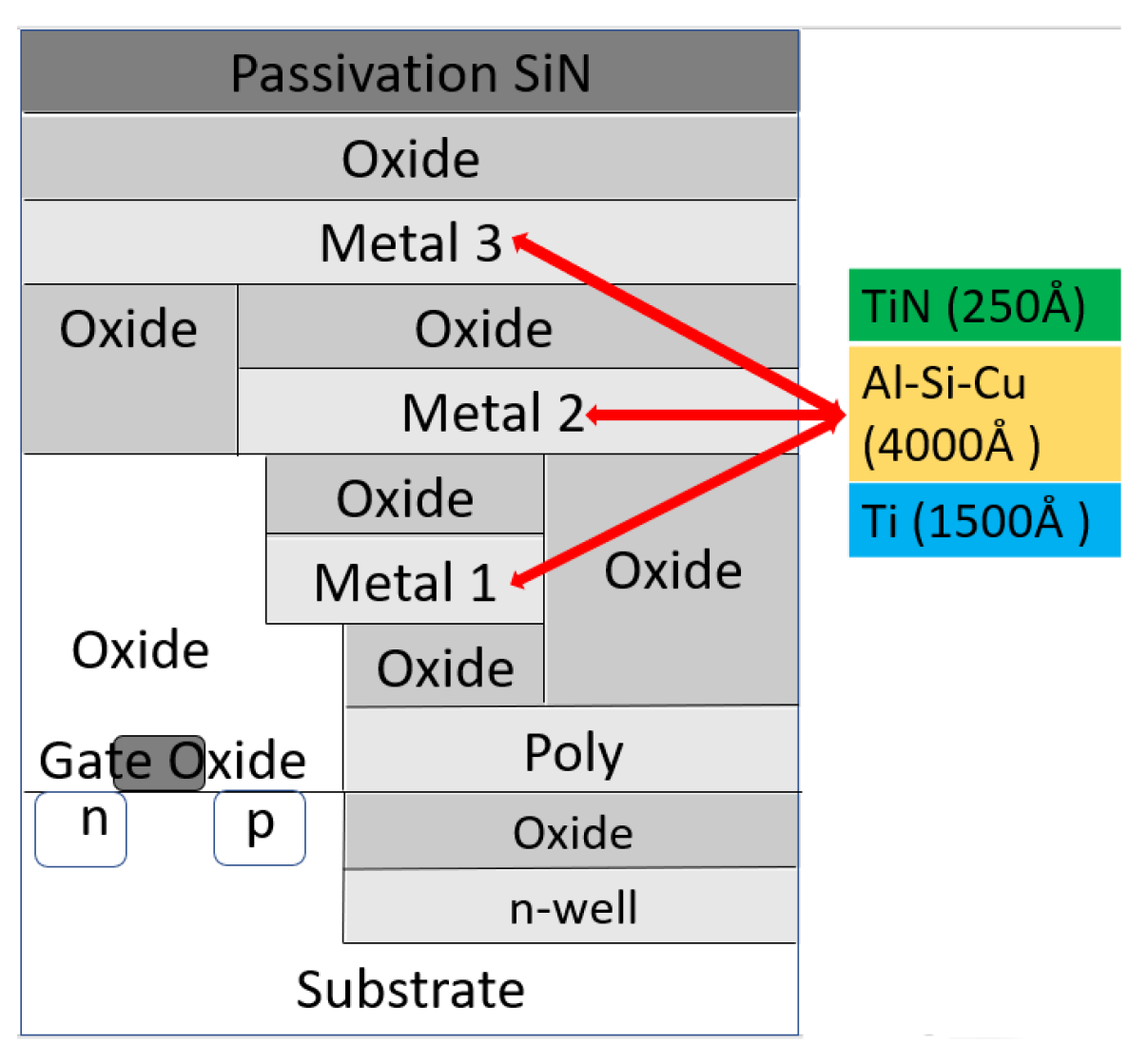
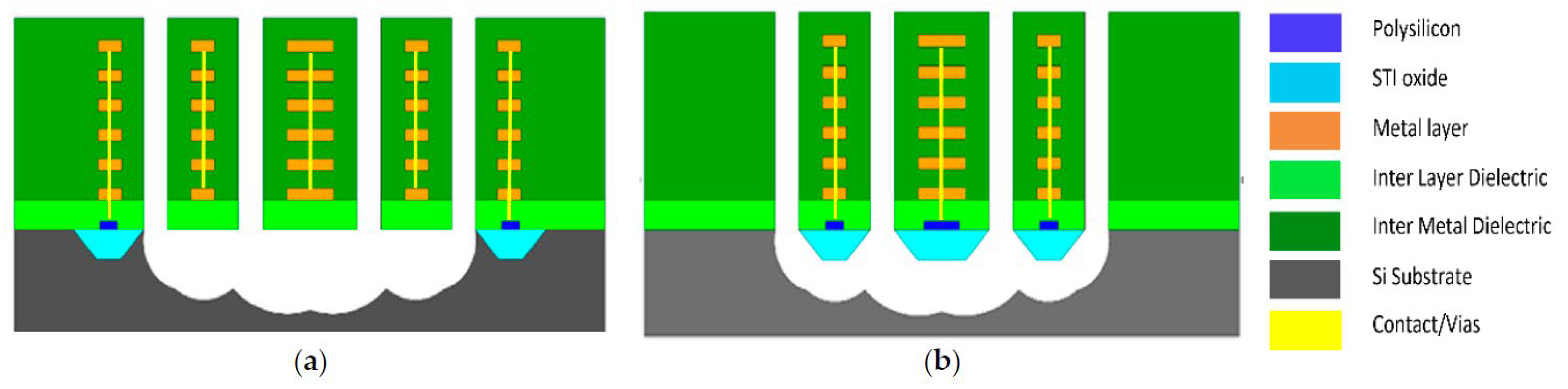
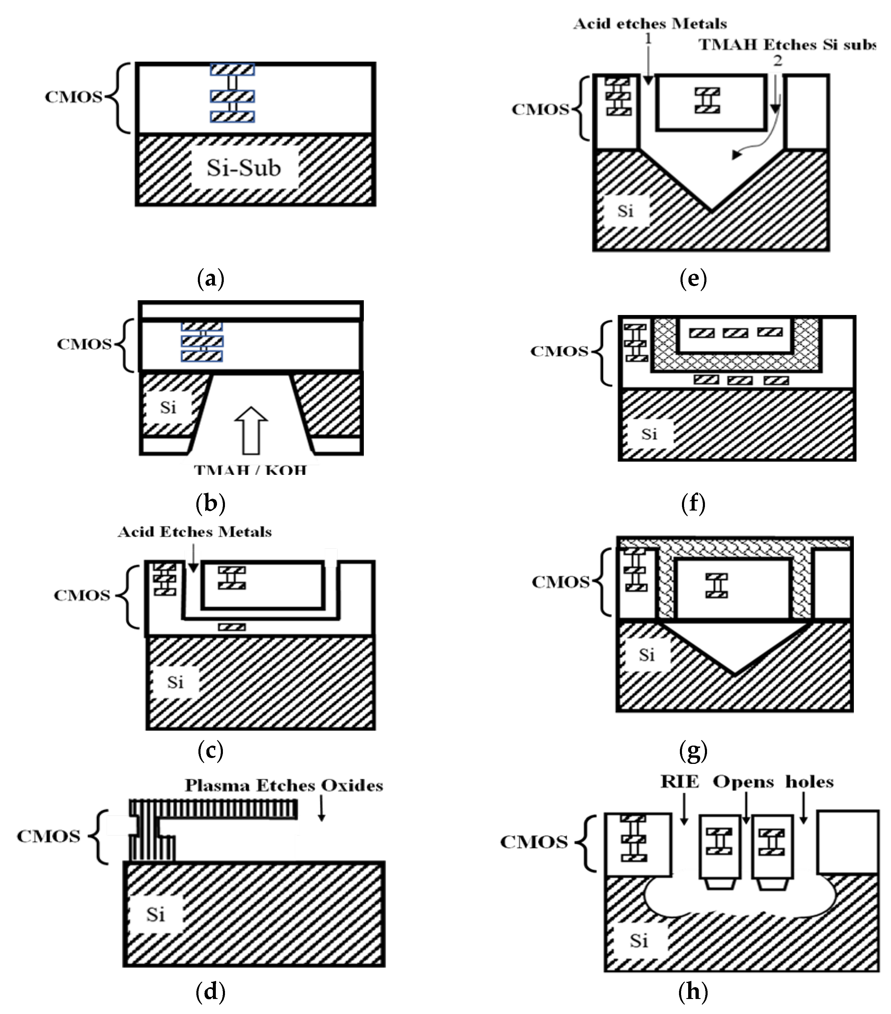
3. Post-Processes of CMOS MEMS Devices

The structures on general ICs are stacked densely and seamlessly. However, for most microsensors, freestanding membranes or suspension bridges are often required. MEMS post-processes help to release these freestanding microstructures after CMOS foundry service. Figure 5 shows all the different post-processes ever developed.
Figure 5a shows the CMOS standard process, which is composed of four kinds of different thin films including silicon nitride (Si3N4), silicon dioxide (SiO2), aluminum, and polysilicon on the silicon substrate. The arrangements of thin films in the order from bottom to top are silicon substrate, silicon dioxide, multiple metal layers with their inter-layer dielectrics (ILD), and the final passivation nitride layer on the top. When the semiconductor chip is stacked on the redistribution layer (RDL: metal interconnect that electrically connect one part of the package to another) and may have through holes for partially exposing the RDL, through the holes corresponding to the substrate pads and having conductive material filling through the holes, the uppermost semiconductor chip may have the same elements as the lower semiconductor chip and may be flip-chip bonded through the holes.
During the post-process of Figure 5b for fabricating a membrane, the backside of the silicon substrate was lapped and polished to reduce its thickness from 680 µm to 200 µm. This procedure decreases much time for backside V-groove etching and preserves the aluminum pads from being attacked by the exposed anisotropic etching solution. Then, it adopts low-temperature technology to deposit the masking films on the backside of the substrate. These masking films were 250 °C PECVD silicon nitride and sputtered silicon oxide at near room temperature. The thickness of PECVD silicon nitride is 0.4 μm and the sputtered silicon oxide is 1.2 μm, for example. After the infrared double-sided lithography, the masking film was patterned by reactive ion etching (RIE) with CF4 plasma. The reason for the requirement of low temperature in MEMS post-process is that the CMOS aluminum layers may have problems of spiking or short circuits in an environment with a temperature higher than 350 °C. In the final step, ethylene-diamine pyrocatechol (EDP) or tetra-methyl-ammonium-hydroxide (TMAH) was used as the silicon anisotropic etching solution [117]. Such anisotropic solutions are good in etching the [1] silicon wafers, but etch-stop on the CMOS oxide layer. It also has good selectivity in metal preservation. The disadvantages are that it wastes the wafer area at the slope on the {111} [87,167] plane [161,165]; the backside photolithography needs to use a double-sided mask aligner; the wafer needs to be thinned and have an additional protective layer (PECVD nitride or sputtered oxide) [165].
The above drawbacks of the post-process Figure 5b are due to the backside V-groove etching [161,165]. When a metal layer is well-designed in advance and assigned to be the sacrificial layer in the post-process (Figure 5c), the sacrificial layer will be etched completely from the front side, and the silicon nitride layer will be released as a suspended structure in the micrometer scale. After all, this is a maskless post-process and needs a wet etching only. The sacrificial material is aluminum. Therefore, it is necessary to select an etchant which can remove aluminum selectively. One etchant recipe consisting of phosphoric acid (75%), nitric acid (5%), acetic acid (5%), and deionized (DI) water (15%) is adopted to etch a sacrificial layer at the temperature of 60 °C. Of course, this post-process needs etching holes from the front side to fabricate suspended open structures without difficulties, but it requires a hole-filling process subject to a membrane fabrication.
With the post-process shown in Figure 5d, the metallic suspension bridges can be created from the front side, and the sacrificial material is changed to oxide accordingly. Herein, the plasma etching is performed after the passivation nitride is removed and the top metal layer is exposed. Therefore, the top metal layer is used as the etch-resistant material during the subsequent dry etching that creates the laminated microstructure. Without wet etching, surface tension sticking does not occur, and the laminated-suspension microstructures are achieved. The anisotropic oxide plasma etches through to the silicon substrate by CF4/O2 RIE. By employing the large undercut of SF6 RIE, 2.5 µm width of the beam could be released within 15 min [130].
Figure 5e is for releasing the suspension bridge structure of accelerometers, flowmeters, or infrared thermometers; the layers of the CMOS are opened with patterns and then also soaked in the anisotropic etching solution to attack the silicon substrate frontside.
Choices of highly selective etchants are listed in Table 2 and remove different sacrificial layers including “contact”, “metal”, and “via”. The etchant-(1) is used to etch the Ti-W alloy (the “contact” and “via” layers). Etchant-(2) is used to remove the aluminum (the “metal” layer.) The sacrificial layers etching process involves: first, clean the CMOS sensor die with the acetone, isopropyl alcohol (IPA), and DI water. Second, the die is immersed in etchant-(2) maintained at 70 °C for 50 min. Third, immerse the die in etchant-(1), maintaining the temperature at 70 °C for 30 min. Repeat the etching-(1) and etching-(2) for five times to remove the sacrificial metal layers clearly. The silicon anisotropic etching may use the etchant-(3) finally to release the diaphragm.
An inverted pyramid or V-groove is formed under the suspension bridge floating structure by this post-process of front-side etching herein. The good point is that there is no hole-enlarging problem for the {111} slope, and the depth of the V-groove does not have to be etched through the silicon substrate as in the second type post-process. The disadvantage is that the cross-section of the multi-layer suspension bridge structure is easily invaded into the gaps between the layers by the etching solution of the silicon crystal, destroying the deposited embedded metal and polysilicon layers. In addition, when the CMOS foundry is completed, the silicon nitride protective layer is patterned at the metal contacts (I/O pads) on the front side of the wafer [168]. Therefore, when the silicon crystal is anisotropically etched, care should be taken to ensure the selectivity of the etchant to silicon and metals. In the formation of the bridge floating plate or even the first post-process on membrane, the metal contacts cannot also be sacrificed. Usually, the first two post-processes use EDP or TMAH [88].
An example of the CMOS post-process of Figure 5f is, for fabricating the magnetic coil [90], in view of the production of magnetic coils and based on the consideration of reducing the magnetic loss of general semiconductor materials, a micro-electroforming process must be added after the post-process Figure 5c. The coil structure is basically divided into a ferro-core and a conductive winding around it. The metal layers (M1 and M3 in Figure 1) and the via of the CMOS process can be re-wrapped to form a 3D coil, and the center core needs to be ferromagnetic. The main spirit of electroforming is that the metal layer M2 in Figure 1 is designed as a core shape, but the two ends are exposed. After all the CMOS structures are grown and stacked, the M2 aluminum core of the central core portion is etched by an acid solution firstly, and a microchannel is formed. The polysilicon or titanium is used as a seeding layer to infiltrate the iron–nickel electroforming liquid, and the electroformed iron-nickel alloy is grown and filled into micro-channels. In the channel, it acts as a high permeability iron core microstructure.
Figure 5g is after the post-process of Figure 5e and works for fabricating membranes for pressure sensors. Then, the CMOS sensor die is packaged by the wire-bonding and cavity sealing before testing. For ensuring the well function of the CMOS pressure sensor, one must seal etching holes on the diaphragm after the post etching to isolate the cavity from the ambient environment. The authors used a reversible thermoplastic gelatin to seal the etching holes [87,88]. A room-temperature growth parylene is also suitable for sealing the etching holes in a dry manner [89].
The post-process Figure 5h is the UMC-0.18 μm CMOS MEMS process of Figure 4, which includes the anisotropic silicon oxide etching process and isotropic silicon etching process. The post-process included an anisotropic dry etching with CHF3/O2 RIE to remove the sacrificial oxide layer and an isotropic dry etching with gas-phase XeF2 to etch the silicon substrate. The isotropic XeF2 undercut etching is for the MEMS open area. The detailed explanation has been given in Figure 2, Figure 3 and Figure 4. STI oxide is used to protect polysilicon during XeF2 etching [96,97,102,122].

4. Case Study of Flow Sensor Using UMC 0.18 µm CMOS MEMS Process

CMOS MEMS technology has been utilized in recent times for the fabrication of low-cost micromachined flow sensors [4,62,161,168,169,170]. Flow sensors are the key elements in most systems for monitoring and controlling fluid flows. With the design of MEMS thermal flow sensors, unprecedented performances, such as ultra-wide measurement ranges, low power consumptions, and extreme size miniaturization were targeted, although several critical issues remain still to be solved.
After obtaining the consent of CIC, the authors developed the manufacturing flow of CMOS MEMS sensors, as shown in Figure 6. In the design system, after creating a library, one can choose schematic or Virtuoso according to our need. The schematic editor used in this case is called Composer, ADS. The model simulator used is H-spice, Spectre. The simulator can run the Netlist pre- and post-simulation after verification being performed in Calibre.

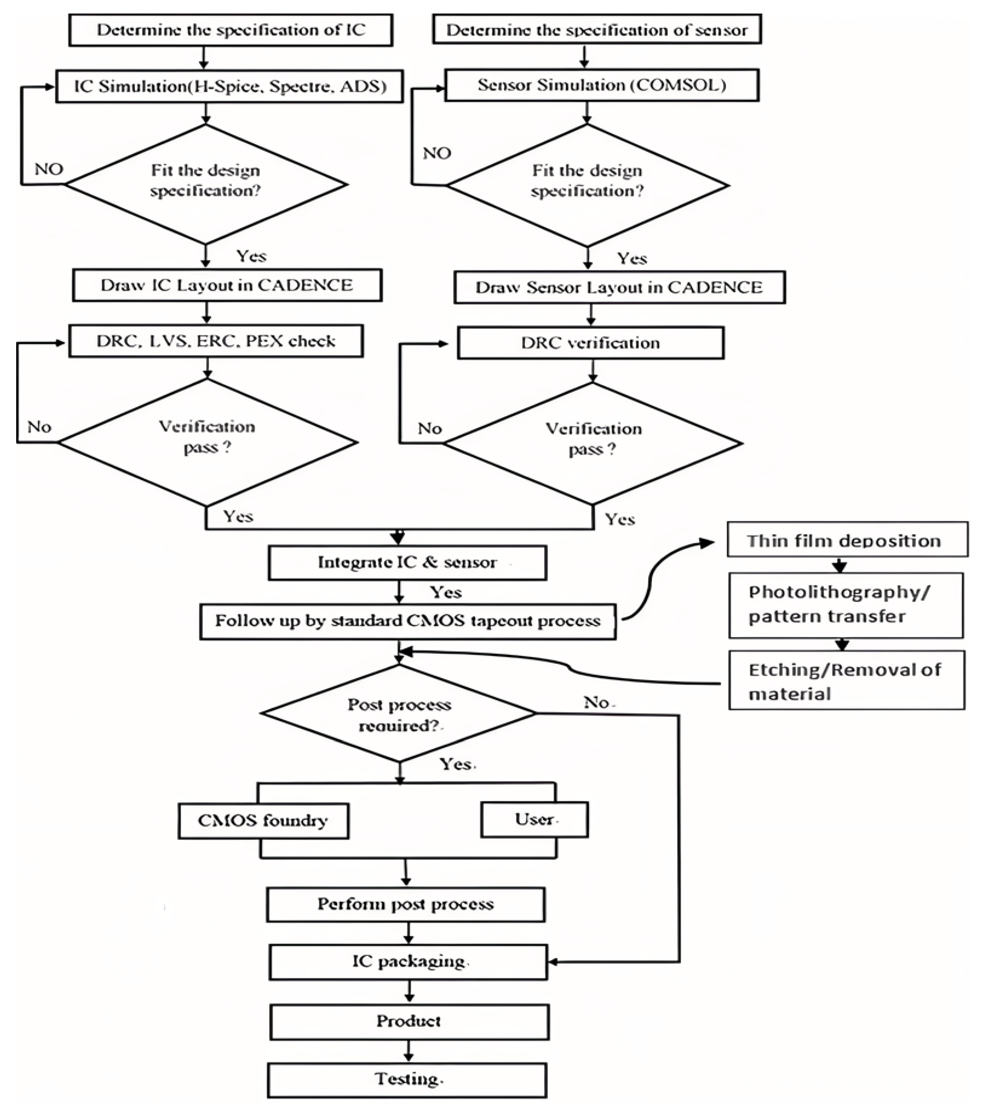
4.1. CMOS MEMS Sensor Design Flow

In the following, the authors took the flow sensor design as an example to verify the CMOS MEMS process of Figure 6. The work builds on a fabrication process reported at Transducers-2021 [96], revealing that CMOS MEMS technology can generate minimal space utilization micromachined flow sensors. The flow sensor was designed with a self-heating half-bridge RTD or a hot wire that did not use any heater during the operation. This concise device size can be in the range of 100 μm and ideally fabricated by the CMOS MEMS process. The amplifier was also added later to the sensor design. Numerous micromachined thermal flow sensors have been surveyed for different materials and applications including battery-free, wireless devices, nano mechanical sensor [171], infrared sensors [172,173,174,175,176], and calorimetric sensors [144,177,178,179,180]. The high-quality CMOS foundry services provided by TSMC and UMC foundry were highly welcome over the past two decades. The CMOS MEMS foundry is therefore one of the best candidates so far to implement the new MEMS sensor design and fabrication. Another major advantage for this kind of flow sensor is its low power consumption.

4.2. Flow Sensor Design

Initially, the design of the flow sensor was conducted with a self-heating or hot-wire type where it did not use any additional heater during the operation. The self-heating of the RTD bridge circuit was originally a noise problem and a shortcoming to the thermal flow sensors. We conventionally needed to eliminate this noise by ways of reducing excitation (sensing) current or using pulse measurements. We only adopted a bridge circuit composing of 2 RTDs, R1 and R2, in series, as shown in Figure 7a. The self-heating voltage V0 is no more a noise, but the bias to the RTD half bridge is necessary for the device operation. Resistor R1 is on the substrate, and R2 is on the MEMS cavity or the free standing plate region, which provides good thermal isolation [96]. T1 is the local temperature on the substrate, and T2 is on the MEMS cavity with air gap underneath, accordingly. Figure 7b shows the layout diagram of the flow sensor with an amplifier circuit drawn in Cadence software. The amplifier circuit will be mentioned in Section 4.3 [180].
By the one-dimensional (1D), steady state thermal resistance analysis of heat conduction about the silicon substrate and the MEMS cavity area, the simplified models are assumed in Figure 7c,d, respectively. The heating or bias power q from the RTDs diffuses to ambient by ways of the convective cooling on the top and the conduction on the bottom (“//” means two thermal resistances in parallel). Using the Fourier law of heat conduction [181], the temperature differences ΔT1,2 = (T1,2T) related to the heat transfer rate q are shown in Equations (1) and (2).
T 1 T ( L S i k S i A ) / / ( 1 h A + L M O k M O A ) = q = V 0 2 4 R 0
T 2 T ( L S i k S i A + L S T I k S i O 2 A + L c a k f A ) / / ( 1 h A + L M O k M O A ) = q = V 0 2 4 R 0
In addition, the heat transfer coefficient h relates to the flow speed U by the laminar boundary layer theory, as in Equation (3) or Equation (4), subject to a flat plate under the medium value of the Reynolds number flow [182]. Substituting Equation (4) into Equations (1) and (2) can correlate the temperature difference and the flow speed.
N u = h x k f = 0.664 ( R e 1 / 2 ) ( P r 1 / 3 ) = 0.664 P r 1 / 3 U x ν
h = 0.664 k f P r 1 / 3 U ν x
where
A: Area of chip (300 μm × 250 μm)
Δ T : Temperature difference
h: Convective heat transfer coefficient.
Lsi: Thickness of silicon (400 μm)
LMO: Thickness of metal (9.76 μm)
LSTI: Thickness of STI (0.4 μm)
Lca: Thickness of air cavity (45 μm)
Kf: Thermal conductivity of air (0.025 W/m K)
Ksi: Thermal conductivity of silicon (148 W/m K)
KMO: Thermal conductivity of metal (237 W/m K)
KsiO2: Thermal conductivity of silicon dioxide (1.3 W/m K)
Nu: Nusselt number
Pr: Prandtl number (0.73 for air)
q: Heat transfer rate
Re: Reynolds number
R0: Heater resistance in ohm
T 1 ,   2 : Surface temperature of positions 1 and 2
T : Ambient temperature (25 °C)
U : Freestream flow speed (1–10 m/s)
Vo: Power supply (1.8 V)
ν: Kinematic viscosity (viscosity/density) of the air at 25 °C (15.52 × 10⁻⁶ m2/s)
x: Sensor bridge length occupied by the sensor on the chip. (167.5 μm)
We have taken R0 as the design resistance value (1 kΩ) of one RTD with the temperature coefficient of resistance (TCR = 2.97−3/°C). As the flow speed increases across the biased RTDs, both RTDs have a temperature drop, but the cooling effect of R1 on the silicon substrate is better than R2 on the MEMS cavity with air gap thermal isolation. So, the temperature difference ∆T2 = T2T of R2 is greater than ∆T1 = T1 − T of R1. The values of R1 and R2 after application of flow speed can be shown below.
R 2 = R 0 1 + T C R T 2
R 1 = R 0 1 + T C R T 1
The output voltage of the half-bridge is therefore approximated as Equation (5) following the temperature difference between two RTDs by the voltage divider formula and the binominal theorem, as below.
V o u t / V 0 0.5 1 + T C R 0.5 T 2 T 1
Combining Equations (1), (2), (4), and (7), we can correlate the output voltage Vout and flow speed U. By this theoretical formulation, the output voltage change is first estimated as 0.125–0.5 mV by 1 V DC bias per 1 m/s flow speed change if the TCR values are 500–2000 ppm/K. The authors moreover predict the theoretical output voltage in Figure 8a.
Based on the UMC 0.18 μm standard 1P6M CMOS foundry with the MEMS post-process shown in Figure 4, the flow sensor was implemented with cavities underneath the freestanding plates of multiple metals M1–M6 and ILD.
According to the theoretical values of Figure 8a, the output voltage Figure 8b of the fabricated flow sensor by UMC 0.18 μm MEMS process was verified by a wind tunnel facility in Figure 8c. Preliminarily, the theoretical sensitivity of 113 µV/V/(m/s)/mW is near to the measured sensitivity 138 µV/V/(m/s)/mW under the flow speed of 15 m/s; the linearity of the measured output voltage is obviously better than the theoretical one. The reason why the sensitivity of the theoretical output voltage was underestimated is that the actual flow speed was lower than the freestream speed, U . The amount of flow speed retarding from the freestream inside the boundary layer of the flow sensor surface could be furthermore investigated by FEAs such as ANSYS or COMSOL. The 18% sensitivity difference between the theoretical and experimental data corresponds to factors such as packaging design and resistance variation during the semiconductor fabrication.

4.3. Instrumentation Amplifier Design

The instrumentation amplifier (In-Amp or IA) shown in Figure 9a can amplify the output signal of the above CMOS MEMS flow sensors. MEMS flow sensors are often based on temperature detection. For most materials, the electrical resistivity changes with temperature. IA is a type of differential amplifier that has been outfitted with input buffer amplifiers, which eliminate the need for input impedance matching and thus make the amplifier particularly suitable for use in measurement and test equipment. Additional characteristics include a very low DC offset, low drift, low noise, very high open-loop gain, very high common-mode rejection ratio (CMRR), and very high input impedances. IAs are used where great accuracy and stability of the circuit for short-term and long-term are required [183]. Using materials with the appropriate TCR permits us to achieve a high sensitivity to temperature changes and thus to flow speed. Integration on the same chip will contribute to a more precise output, sources of error will be minimized, and fault-prone solder points will be eliminated [184].
The IA layout consists of three operational amplifiers circuits in Figure 9b, which always has difficulty in equalizing two R1~R3 values in the layout of Figure 9a for real CMOS fabrication. It therefore gives a testing result of 30 dB gain only under the bandwidth of 10 kHz. The DC level also deviates from the design value of V0/2. With the supply voltage as V0 = 1.8 V and reference voltage as 1 V, the total current consumption is 1.335 mA.
The half-bridge output voltage of Equation (5) has a DC level of 0.5 V0. Although it does not affect the sensitivity, the DC level should be reset to zero. Using the IA of Figure 9, the DC level is easy to eliminate by assigning the V1 = sensor output voltage and V2 = 0.5 V0. Again, due to the difficulty in in equalizing two R1~R3 values in the layout of Figure 9a for real CMOS fabrication, the DC level cannot be exactly eliminated. This deficiency can be observed from the output voltage of the amplified output voltage of the flow sensor in Figure 8d.
With the on-chip integration IA of Figure 9, the authors redid the wind tunnel testing on the CMOS MEMS flow sensor. The overall sensitivity of the integrated flow sensor was improved to 1388 µV/V/(m/s)/mW for a flow speed ranging within 0–5 m/s, as plotted in Figure 8d. The voltage gain discussion will be addressed in the next section.

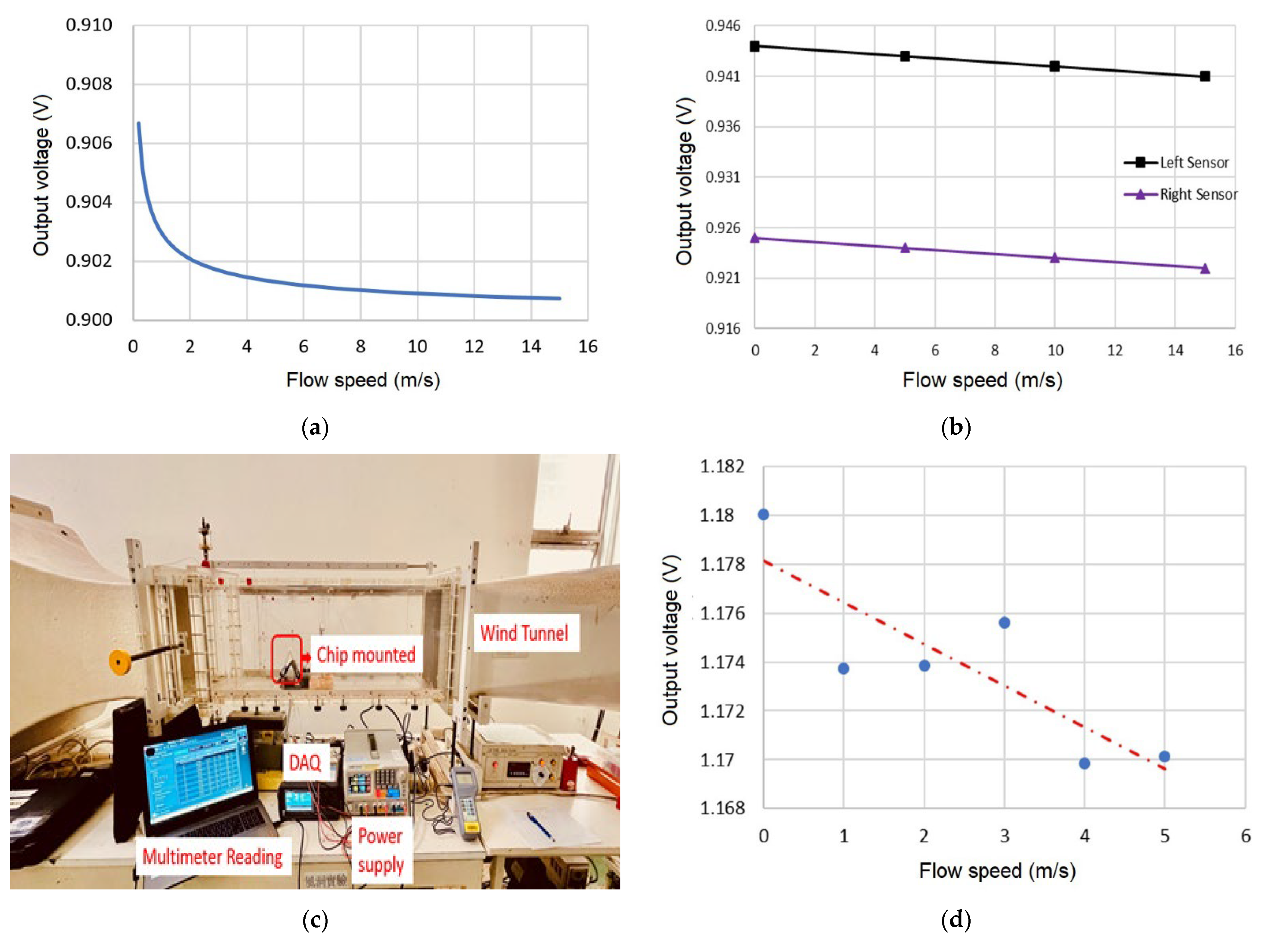
5. Results and Discussions

The following advantages and technical issues of CMOS MEMS technology are discussed by the case study of flow sensors:

5.1. Smaller Device Size

Technology has been pushed to the point that we can build a device so small that it can hardly be seen with our human eye. The typical size of MEMS devices is usually measured in micrometers. Using similar fabrication techniques as in building ICs, people are now able to build sensors and actuators on the same microscopic level with the processor chip. Measured in micrometers, almost all MEMS sensors and actuators can be batch-produced together on the same chip with circuitry. They indeed compose a system on a chip as small as possible according to the CMOS technology now [153].
The flow sensor is made with the latest U18MEMS CMOS MEMS process, which was discussed in Section 4.2. The dimensions of the flow sensor were miniaturized to save the chip area and achieve an acceptable sensitivity and linearity. The sensor size herein was 300 μm × 250 μm in Figure 7a,b, which is smaller than many prior arts’. Within the flow speed range of 0–15 m/s in a wind tunnel, a normalized sensitivity of this small CMOS MEMS sensor was obtained as 138 μV/V/(m/s)/mW, which is with the same order of magnitude to the best value of 160 μV/V/(m/s)/mW of the prior arts [59,60,62,76,93,94,97,185].

5.2. Less Power Consumption

With enhanced sensitivity and less power consumption with only one RTD self-dissipating power of 0.81 mW, we can say that signal-to-noise ratio (SNR) is better as the sensitivity was able to measure without any readout circuit [96,186]. In a digital viewpoint, the small voltage swing results in a small noise margin. In the analog domain, the strength of signal level is weakened due to the low supply voltage. The total power consumed by the flow sensor with IA is 3.24 mW. Other designs such as calorimetric-type flow sensors consume more power due to the additional center heater for adjusting the output performance [59,93,94,181].

5.3. Enhancing the Sensing Sensitivity by On-Chip Amplifiers

Adding on-chip amplification circuits to the RTD flow sensors may result in a different behavior of the sensor output sensitivity compared to the one without amplifier circuitry. Addressing the above challenge requires the collaboration of MEMS and analog circuit design engineers. The case study of the self-heating RTD flow sensor alone gives a normalized output sensitivity of 138 µV/V/(m/s)/mW under the flow speed of 15 m/s. With the measured gain of IA as 30 dB calibrated at 10 kHz, and by integrating it into the self-heating RTD sensor, the overall sensitivity is improved to 1388 µV/V/(m/s)/mW for flow speeds ranging within 0–5 m/s in Figure 8d. The overall voltage gain is 20 dB smaller than the calibrated value of 30 dB. In other words, the CMOS flow sensor with on-chip IA was observed to have 10x better sensitivity.

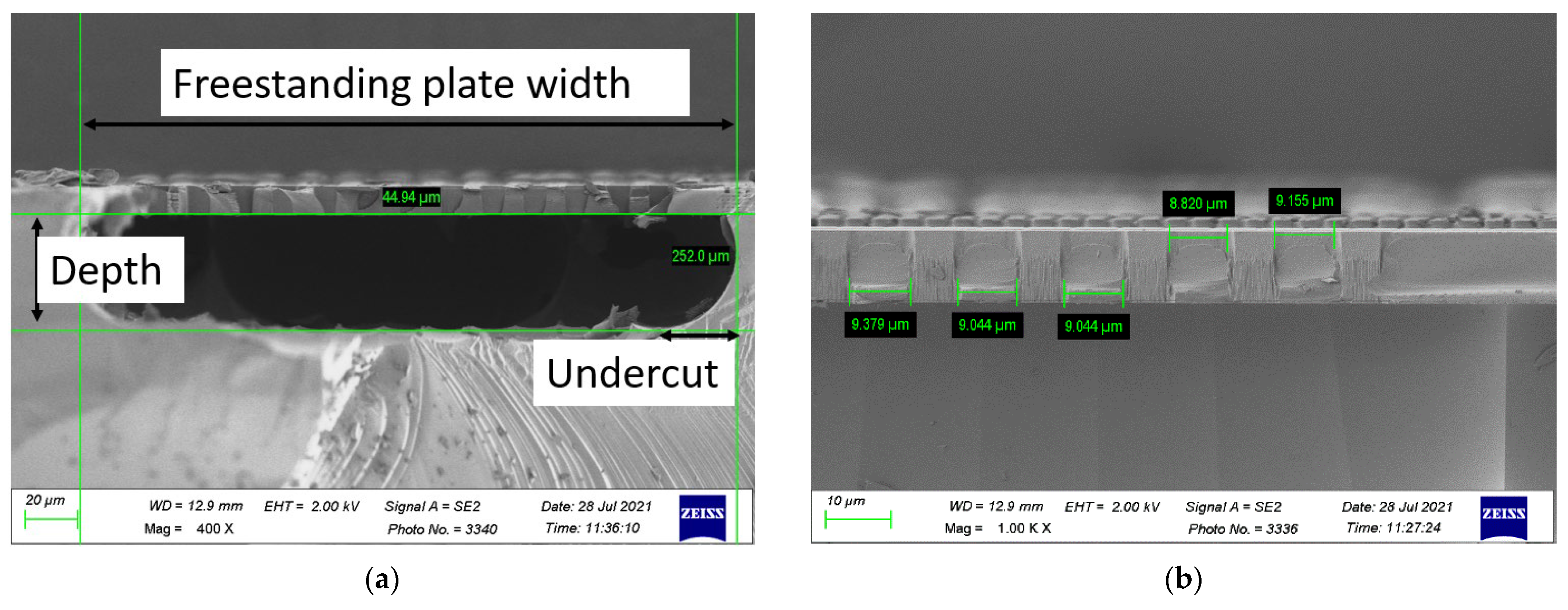
5.4. Other Technical Issues of CMOS MEMS Process

5.4.1. Residual Stress and Resistivity of the CMOS Layers

In the surface micromachining, reducing the residual stress of the microstructure is an issue involving the warping of the microstructure after its release and suspension by removing the sacrificial layer, or even causing the adhesion or stiction to the silicon substrate. The phenomenon of the device failure is that the suspended micro structures, after CMOS fabrication and post-processing, have some unavoidable residual stress where the CMOS process is not able to adjust the process parameters as the polysilicon structure layer is grown in the LPCVD of surface micromachining. The residual stress problem can be minimized by avoiding the cantilever structure (because the free end will arbitrarily turn up or bend down) or I-beam configuration [130]. Instead, one can use a thin bridge or membrane design (e.g., Figure 2, Figure 3 and Figure 4) to resist the residual stress by the rigidity of the structure. The residual stress state of each structural layer of CMOS materials, including information such as tensile stress or compressive stress, magnitude, etc. cannot be obtained from the technology file of the foundry service. Therefore, a concept of “test key” may be necessary to develop the mechanical parameter monitoring technology of the semiconductor process by an onsite sensing way [37,92,165]. The microstructure of the in-situ gauge or test key showing mechanical behavior such as residual stress/strain and mechanical properties such as Young’s modulus and Poisson’s ratio.
Similarly, the resistivity or TCR values of polysilicon and metal layers in CMOS layers cannot be identified very accurately from the technology file of the foundry service, either. This is the reason why the theoretical prediction of 1D thermal resistance model in Figure 8a deviates away from the measured data Figure 8b so obviously. For perfecting the CMOS MEMS sensor design in the future, allocating some small area with test keys for in situ measuring the resistivity and TCR values is mandatory.

5.4.2. Monolithic Integration of MEMS and CMOS Circuits

Finally, the ideal monolithic MEMS device, although it can be directly implemented in a CMOS foundry service, has some problems that need to be solved. The biggest difficulty lies in the integration of the circuit functions because the IC design software cannot directly simulate the output signal changes caused by the MEMS sensor. For example, the sensing capacitor or RTD is only a value-fixed capacitance or resistance in Cadence. H-Spice may predict the relationship between the pre-drive bias voltage and the output voltage but cannot capture the model in which the sensing capacitance or resistance changes.
The so-called “on chip” in the circuit function still lacks real integration with MEMS sensors. It means that only the MEMS sensing element and the signal processing circuit are fabricated on the same silicon chip physically (for the CMOS MEMS chip, the process and the material are already compatible). However, there is no circuit model available for the MEMS devices. Therefore, the overall system optimization of MEMS and IC devices cannot be performed yet in the Cadence software so far. In the existing operation of the Cadence software, the signal processing circuit first completes all the verification procedures, and then it is put together with the layout of the MEMS sensor that is verified by the DRC only. Finally, it is sent directly to the foundry production. After the foundry service, the basic functions of ICs are firstly tested, and then the “hybrid” connection is performed nearest to the wire bonding pads to realize the physical sensor test totally. (This is what the authors actually have completed about the integration testing of the amplified flow sensor output in Figure 8d). For the successful integration of MEMS and circuitry function by CMOS MEMS in the future, there are several difficulties needed to be overcome.

6. Conclusions

The authors have summarized the CMOS MEMS techniques and processes used during the design of various kinds of sensors. Design applications mentioned in this paper such as flow sensor and instrumentation amplifier (IA) were made using the latest U18MEMS process, which is a combination of the UMC 0.18 µm 1P6M process along with the MEMS post-process of XeF2 etching by TSRI. Moreover, a potential sensors system-on-chip (SOC) through CMOS–MEMS technology becomes feasible to be widely implemented in smart living communities. The latest process shows that by employing CMOS-based fabrication technologies, we can monolithically integrate MEMS devices and their associated application-specific ICs, thereby enhancing their overall performance as compared with their stand-alone counterparts. As a case study herein, the CMOS MEMS flow sensor with on-chip IA was observed to have 10x better sensitivity than a flow sensor alone. This self-heating RTD bridge alone gives a normalized output sensitivity of 138 µV/V/(m/s)/mW for a flow speed under 15 m/s. With the measured gain of IA as 30 dB, and by integrating it with the afore-mentioned flow sensor, the overall sensitivity is improved to 1388 µV/V/(m/s)/mW for a flow speed within 0–5 m/s. The integrated voltage gain is observed as 20 dB subject to DC air-flow impinging. This foundry service of CMOS–MEMS processes will be useful as it leads to a smaller size and less power consumption with enhanced sensitivity response and could be widely applied to more smart or intelligent fields, e.g., the operation monitoring of wind turbines and biomimetic flights, etc. Although this study aimed to report the development processes of past and present CMOS MEMS processes, the author additionally validates the current processes and techniques with a design of flow sensor while using polysilicon as the design material so that it can then be implemented in any flow-sensing applications. It is important to note that this may be an appropriate moment to list a few more semiconductor materials for their high voltage, high frequency applications. In the upcoming years, many small companies, serving niche markets with special processes using different material such as SiC, GaN, etc., may make medium-cost IC’s and sensors and will coexist alongside a few large IC industries, producing inexpensive smart sensor systems for mass markets, which may indeed fulfill the current high demand, leading to chip shortage. CMOS MEMS processes have already become an integral part of all the electronic devices, vehicles, biomedical devices, etc., and looks to be a promising and fruitful field of scientific research for the years to come.

Author Contributions

Conceptualization, L.-J.Y.; methodology, L.-J.Y.; software, R.W.; validation, L.-J.Y., R.W. and H.-Y.S.; formal analysis, L.-J.Y., Y.-K.L. and R.W.; investigation, R.W.; resources, H.-Y.S.; data curation, R.W.; writing—original draft preparation, R.W.; writing—review and editing, L.-J.Y.; visualization, L.-J.Y. and R.W.; supervision, L.-J.Y. and H.-Y.S.; project administration, L.-J.Y.; funding acquisition, L.-J.Y. All authors have read and agreed to the published version of the manuscript.

Funding

This work is supported by Taiwan’s Ministry of Science and Technology by the project grant numbers 109-2221-E-032-002-MY2, 109-2221-E-032-001-MY3.

Institutional Review Board Statement

Not applicable.

Informed Consent Statement

Not applicable.

Acknowledgments

The technical help from Chandrashekhar Tasupalli, Vivek Jabaraj Joseph, Neethish Kumar Unnam, and Paritala Veeranjaneyulu are all acknowledged. Additionally, we express thanks to the Chemical Engineering Department of Tamkang University for providing SEM service.

Conflicts of Interest

The authors declare no conflict of interest.

References

  1. Feynman, R.P. There’s plenty of room at the bottom. Eng. Sci. 1959, 23, 22–36. [Google Scholar]
  2. Shockley, W. The Theory of p-n Junctions in Semiconductors and p-n Junction Transistors. Bell Syst. Tech. J. 1949, 28, 435–489. [Google Scholar] [CrossRef]
  3. Bardeen, J.; Brattain, W.H. Physical principles involved in transistor action. Phys. Rev. 1949, 75, 1208. [Google Scholar] [CrossRef]
  4. Ghodssi, R.; Lin, P. MEMS Materials and Processes Handbook; Springer Science & Business Media: Berlin/Heidelberg, Germany, 2011; Volume 1. [Google Scholar]
  5. Smith, C.S. Piezoresistance effect in germanium and silicon. Phys. Rev. 1954, 94, 42. [Google Scholar] [CrossRef]
  6. Petersen, K.E. Silicon as a mechanical material. Proc. IEEE 1982, 70, 420–457. [Google Scholar] [CrossRef]
  7. Nathanson, H.C.; Newell, W.E.; Wickstrom, R.A.; Davis, J.R. The resonant gate transistor. IEEE Trans. Electron Devices 1967, 14, 117–133. [Google Scholar] [CrossRef]
  8. Faggin, F.; Hoff, M.E.; Mazor, S.; Shima, M. The History of the 4004. IEEE Micro. 1996, 16, 10–20. [Google Scholar] [CrossRef]
  9. Fan, L.-S.; Tai, Y.-C.; Muller, R.S. IC-processed electrostatic micromotors. Sens. Actuators 1989, 20, 41–47. [Google Scholar] [CrossRef] [Green Version]
  10. Muller, R.; Conragan, J. Transducer action in a metal-insulator-piezoelectric-semiconductor trIODE. Appl. Phys. Lett. 1965, 6, 83–85. [Google Scholar] [CrossRef]
  11. Sangster, F.L.J.; Teer, K. Bucket-brigade electronics: New possibilities for delay, time-axis conversion, and scanning. IEEE J. Solid-State Circuits 1969, 4, 131–136. [Google Scholar] [CrossRef]
  12. Boyle, W.S.; Smith, G.E. Charge coupled semiconductor devices. Bell Syst. Tech. J. 1970, 49, 587–593. [Google Scholar] [CrossRef]
  13. Samaun, S.; Wise, K.; Nielsen, E.; Angell, J. An IC piezoresistive pressure sensor for biomedical instrumentation. In Proceedings of the 1971 IEEE International Solid-State Circuits Conference, Digest of Technical Papers, Philadelphia, PA, USA, 17–19 February 1971; pp. 104–105. [Google Scholar]
  14. Terry, S.C.; Jerman, J.H.; Angell, J.B. A gas chromatographic air analyzer fabricated on a silicon wafer. IEEE Trans. Electron Devices 1979, 26, 1880–1886. [Google Scholar] [CrossRef]
  15. Wise, K.D.; Angell, J.B.; Starr, A. An integrated-circuit approach to extracellular microelectrodes. IEEE Trans. Biomed. Eng. 1970, 17, 238–247. [Google Scholar] [CrossRef] [Green Version]
  16. Borky, J.; Wise, K.D. Integrated signal conditioning for silicon pressure sensors. IEEE Trans. Electron Devices 1979, 26, 1906–1910. [Google Scholar] [CrossRef]
  17. Matsuo, T.; Wise, K.D. An integrated field-effect electrode for biopotential recording. IEEE Trans. Biomed. Eng. 1974, BME-21, 485–487. [Google Scholar] [CrossRef]
  18. Najafi, K.; Wise, K.; Mochizuki, T. A high-yield IC-compatible multichannel recording array. IEEE Trans. Electron Devices 1985, 32, 1206–1211. [Google Scholar] [CrossRef]
  19. Yoon, E.; Wise, K.D. A multi-element monolithic mass flowmeter with on-chip CMOS readout electronics. In Proceedings of the IEEE 4th Technical Digest on Solid-State Sensor and Actuator Workshop, Island, SC, USA, 4–7 June 1990; pp. 161–164. [Google Scholar]
  20. Ko, W.H.; Bao, M.-H.; Hong, Y.-D. A high-sensitivity integrated-circuit capacitive pressure transducer. IEEE Trans. Electron Devices 1982, 29, 48–56. [Google Scholar] [CrossRef]
  21. Ko, W.H.; Hynecek, J.; Boettcher, S.F. Development of a miniature pressure transducer for biomedical applications. IEEE Trans. Electron Devices 1979, 26, 1896–1905. [Google Scholar] [CrossRef]
  22. Wen, C.-C.; Chen, T.; Zemel, J. Gate-controlled diodes for ionic concentration measurement. IEEE Trans. Electron Devices 1979, 26, 1945–1951. [Google Scholar]
  23. Lundström, K.; Shivaraman, M.; Svensson, C. A hydrogen-sensitive Pd-gate MOS transistor. J. Appl. Phys. 1975, 46, 3876–3881. [Google Scholar] [CrossRef]
  24. Fischer, A.C.; Forsberg, F.; Lapisa, M.; Bleiker, S.J.; Stemme, G.; Roxhed, N.; Niklaus, F. Integrating mems and ics. Microsyst. Nanoeng. 2015, 1, 1–16. [Google Scholar] [CrossRef] [Green Version]
  25. Senturia, S. Microfabricated structures for the measurement of mechanical properties and adhesion of thin films. In Proceedings of the Proc Transducers, Tokyo, Japan, 2–5 June 1987; pp. 11–16. [Google Scholar]
  26. Van Putten, A.; Middelhoek, S. Integrated silicon anemometer. Electron. Lett. 1974, 10, 425–426. [Google Scholar] [CrossRef]
  27. Bergveld, P. Development of an ion-sensitive solid-state device for neurophysiological measurements. IEEE Trans. Biomed. Eng. 1970, 17, 70–71. [Google Scholar] [CrossRef]
  28. Reyntjens, S.; Puers, R. A review of focused ion beam applications in microsystem technology. J. Micromechanics Microengineering 2001, 11, 287. [Google Scholar] [CrossRef]
  29. Baltes, H.; Göpel, W.; Hesse, J. Sensors, Update 9; Wiley-VCH: Weinheim, Germany, 2001; Volume 9. [Google Scholar]
  30. Göpel, W.; Anderson, J.; Frankel, D.; Jaehnig, M.; Phillips, K.; Schäfer, J.; Rocker, G. Surface defects of TiO2 (110): A combined XPS, XAES and ELS study. Surf. Sci. 1984, 139, 333–346. [Google Scholar] [CrossRef]
  31. Göpel, W.; Rocker, G.; Feierabend, R. Intrinsic defects of Ti O 2 (110): Interaction with chemisorbed O2, H2, CO, and CO2. Phys. Rev. B 1983, 28, 3427. [Google Scholar] [CrossRef]
  32. Krötz, G.; Möller, H.; Eickhoff, M.; Zappe, S.; Ziermann, R.; Obermeier, E.; Stoemenos, J. Heteroepitaxial growth of 3C-SiC on SOI for sensor applications. Mater. Sci. Eng. B 1999, 61, 516–521. [Google Scholar] [CrossRef]
  33. Obermeier, E.; Kopystynski, P. Polysilicon as a material for microsensor applications. Sens. Actuators A Phys. 1992, 30, 149–155. [Google Scholar] [CrossRef]
  34. Shaw, K.A.; Zhang, Z.L.; MacDonald, N.C. SCREAM I: A single mask, single-crystal silicon, reactive ion etching process for microelectromechanical structures. Sens. Actuators A Phys. 1994, 40, 63–70. [Google Scholar] [CrossRef]
  35. Dai, C.-L.; Lu, S.-S.; Chang, P.-Z. Design and processing of integrated micro accel-erometers using standard cmos process. J. Chin. Inst. Eng. 1997, 20, 47–55. [Google Scholar] [CrossRef]
  36. Qu, H. CMOS MEMS fabrication technologies and devices. Micromachines 2016, 7, 14. [Google Scholar] [CrossRef] [PubMed] [Green Version]
  37. Dai, C.-L.; Chang, P.-Z. In-situ micro strain gauges for measuring residual strain of three CMOS thin films using only one maskless post-processing step. J. Chin. Inst. Eng. 1997, 20, 539–548. [Google Scholar] [CrossRef]
  38. Tsai, Z.-Y.; Shih, P.-J.; Tsai, Y.-C.; Dai, C.-L. Manufacturing and Testing of Radio Frequency MEMS Switches Using the Complementary Metal Oxide Semiconductor Process. Sensors 2021, 21, 1396. [Google Scholar] [CrossRef] [PubMed]
  39. Baltes, H.; Brand, O.; Hierlemann, A.; Lange, D.; Hagleitner, C. CMOS MEMS-present and future. In Proceedings of the Technical Digest, MEMS 2002 IEEE International Conference, Fifteenth IEEE International Conference on Micro Electro Mechanical Systems (Cat. No. 02CH37266), Las Vegas, NV, USA, 24–24 January 2002; pp. 459–466. [Google Scholar]
  40. Wang, H.-J.; Cheng, T.-Y.; Huang, C.-C.; Su, C.-Y.; Dai, C.-L.; Tsai, Y.-C. High sensitivity and flexible fabric strain sensor based on electrochemical graphene. Jpn. J. Appl. Phys. 2021, 60, SCCD04. [Google Scholar] [CrossRef]
  41. Baltes, H. CMOS as sensor technology. Sens. Actuators A Phys. 1993, 37, 51–56. [Google Scholar] [CrossRef]
  42. Baltes, H.; Brand, O. CMOS-based microsensors and packaging. Sens. Actuators A Phys. 2001, 92, 1–9. [Google Scholar] [CrossRef]
  43. Baltes, H. CMOS micro electro mechanical systems. Sens. Mater. 1997, 9, 331–346. [Google Scholar]
  44. Baltes, H.; Brand, O.; Fedder, G.K.; Hierold, C.; Korvink, J.G.; Tabata, O. Cmos-Mems; John Wiley & Sons: Hoboken, NJ, USA, 2013. [Google Scholar]
  45. Baltes, H.; Brand, O.; Fedder, G.K.; Hierold, C.; Korvink, J.G.; Tabata, O. CMOS-MEMS: Advanced Micro and Nanosystems, Volume 2. CMOS-MEMS: Adv. Micro Nanosyst. 2005, 2, 608. [Google Scholar]
  46. Baltes, H.; Koll, A.; Lange, D. The CMOS MEMS nose-fact or fiction? In Proceedings of the ISIE’97, IEEE International Symposium on Industrial Electronics, Guimaraes, Portugal, 7–11 July 1997; Volume 151, pp. SS152–SS157. [Google Scholar]
  47. Baltes, H.; Paul, O.; Korvink, J.; Schneider, M.; Buhler, J.; Schneeberger, N.; Jaeggi, D.; Malcovati, P.; Hornung, M.; Hiberli, A. IC MEMs Microtransducers. In Proceedings of the International Electron Devices Meeting, Technical Digest, San Francisco, CA, USA, 8–11 December 1996; pp. 521–524. [Google Scholar]
  48. Hagleitner, C.; Hierlemann, A.; Lange, D.; Kummer, A.; Kerness, N.; Brand, O.; Baltes, H. Smart single-chip gas sensor microsystem. Nature 2001, 414, 293–296. [Google Scholar] [CrossRef]
  49. Bousse, L.; De Rooij, N.F.; Bergveld, P. Operation of chemically sensitive field-effect sensors as a function of the insulator-electrolyte interface. IEEE Trans. Electron Devices 1983, 30, 1263–1270. [Google Scholar] [CrossRef]
  50. Popovic, R.S. Hall Effect Devices; CRC Press: Boca Raton, FL, USA, 2003. [Google Scholar]
  51. Eaton, W.P.; Smith, J.H. Micromachined pressure sensors: Review and recent developments. Smart Mater. Struct. 1997, 6, 530. [Google Scholar] [CrossRef]
  52. Dudaicevs, H.; Kandler, M.; Manoli, Y.; Mokwa, W.; Spiegel, E. Surface micromachined pressure sensors with integrated CMOS read-out electronics. Sens. Actuators A Phys. 1994, 43, 157–163. [Google Scholar] [CrossRef]
  53. Chang, P.-Z.; Dai, C.-L. Microstructural fabrication for measuring residual strains of CMOS thin films. Int. J. Jpn. Soc. Precis. Eng. 1999, 33, 135–140. [Google Scholar]
  54. Chang, C.; Dai, C.L.; Chen, J.Y.; Chen, H.; Yen, K.; Chiou, J.H.; Chang, P.Z. A wideband electrostatic microwave switch fabricated by surface micromachining. J. Chin. Inst. Eng. 2000, 23, 781–787. [Google Scholar] [CrossRef]
  55. Tsai, C.-C.; Li, Z.-H.; Lin, Y.-T.; Lu, M.S.-C. A closed-loop controlled CMOS MEMS biaxial scanning mirror for projection displays. IEEE Sens. J. 2019, 20, 242–249. [Google Scholar] [CrossRef]
  56. Pornsin-Sirirak, N.; Liger, M.; Tai, Y.-C.; Ho, S.; Ho, C.-M. Flexible parylene-valved skin for adaptive flow control. In Proceedings of the Technical Digest, MEMS 2002 IEEE International Conference, Fifteenth IEEE International Conference on Micro Electro Mechanical Systems (Cat. No. 02CH37266), Las Vegas, NV, USA, 24–24 January 2002; pp. 101–104. [Google Scholar]
  57. Xu, Y.; Tai, Y.-C.; Huang, A.; Ho, C.-M. IC-integrated flexible shear-stress sensor skin. J. Microelectromechanical Syst. 2003, 12, 740–747. [Google Scholar]
  58. Xu, Y.; Chiu, C.-W.; Jiang, F.; Lin, Q.; Tai, Y.-C. A MEMS multi-sensor chip for gas flow sensing. Sens. Actuators A Phys. 2005, 121, 253–261. [Google Scholar] [CrossRef]
  59. Xu, W.; Song, K.; Ma, S.; Gao, B.; Chiu, Y.; Lee, Y.-K. Theoretical and experimental investigations of thermoresistive micro calorimetric flow sensors fabricated by CMOS MEMS technology. J. Microelectromechanical Syst. 2016, 25, 954–962. [Google Scholar] [CrossRef]
  60. Ahmed, M.; Xu, W.; Mohamad, S.; Duan, M.; Lee, Y.-K.; Bermak, A. Integrated CMOS-MEMS flow sensor with high sensitivity and large flow range. IEEE Sens. J. 2017, 17, 2318–2319. [Google Scholar] [CrossRef]
  61. Liao, S.-H.; Chen, W.-J.; Lu, M.S.-C. A CMOS MEMS capacitive flow sensor for respiratory monitoring. IEEE Sens. J. 2013, 13, 1401–1402. [Google Scholar] [CrossRef]
  62. Xu, W.; Wang, X.; Zhao, X.; Ke, Z.; Lee, Y.-K. An integrated CMOS MEMS gas flow sensor with detection limit towards micrometer per second. In Proceedings of the 2020 IEEE 33rd International Conference on Micro Electro Mechanical Systems (MEMS), Vancouver, Canada, 18–22 January 2020; pp. 200–203. [Google Scholar]
  63. Shen, W.-C.; Shih, P.-J.; Tsai, Y.-C.; Hsu, C.-C.; Dai, C.-L. Low-concentration ammonia gas sensors manufactured using the CMOS–MEMS technique. Micromachines 2020, 11, 92. [Google Scholar] [CrossRef] [Green Version]
  64. Barlow, J.B.; Rae, W.H.; Pope, A. Low-Speed Wind Tunnel Testing; John Wiley & Sons: Hoboken, NJ, USA, 1999. [Google Scholar]
  65. Benedetti, M.; Fontanari, V.; Zonta, D. Structural health monitoring of wind towers: Remote damage detection using strain sensors. Smart Mater. Struct. 2011, 20, 055009. [Google Scholar] [CrossRef]
  66. Yang, W.; Tavner, P.J.; Crabtree, C.J.; Feng, Y.; Qiu, Y. Wind turbine condition monitoring: Technical and commercial challenges. Wind. Energy 2014, 17, 673–693. [Google Scholar] [CrossRef] [Green Version]
  67. Pedersen, M.M.; Larsen, T.J.; Madsen, H.A.; Larsen, G.C. Using wind speed from a blade-mounted flow sensor for power and load assessment on modern wind turbines. Wind. Energy Sci. 2017, 2, 547–567. [Google Scholar] [CrossRef] [Green Version]
  68. Leu, T.; Yu, J.; Miau, J.; Chen, S. MEMS flexible thermal flow sensors for measurement of unsteady flow above a pitching wind turbine blade. Exp. Therm. Fluid Sci. 2016, 77, 167–178. [Google Scholar] [CrossRef]
  69. Yang, L.-J. The micro-air-vehicle Golden Snitch and its figure-of-8 flapping. J. Appl. Sci. Eng. 2012, 15, 197–212. [Google Scholar]
  70. Wei, G.; Bi, Y.; Li, X.; Xu, D.; Xu, W.; Yang, L.-J.; Qin, Y.; Guo, H.; Zhao, X.; Chen, X. Self-powered hybrid flexible nanogenerator and its application in bionic micro aerial vehicles. Nano. Energy 2018, 54, 10–16. [Google Scholar] [CrossRef]
  71. Yang, L.-J.; Tasupalli, C.; Waikhom, R.; Panchal, N. Soap Film Visualization of a 10 cm-Span Flapping Wing. Fluids 2021, 6, 361. [Google Scholar] [CrossRef]
  72. Yang, L.-J.; Esakki, B. Flapping Wing Vehicles: Numerical and Experimental Approach; CRC Press: Boca Raton, FL, USA, 2021. [Google Scholar]
  73. Yang, L.-J.; Esakki, B.; Chandrasekhar, U.; Hung, K.-C.; Cheng, C.-M. Practical flapping mechanisms for 20 cm-span micro air vehicles. Int. J. Micro Air Veh. 2015, 7, 181–202. [Google Scholar] [CrossRef] [Green Version]
  74. Yang, L.-J.; Esakki, B.; Waikhom, R. Inertial Effect on the Time-Averaged Lift of Flapping Wings. J. Appl. Sci. Eng. 2020, 23, 357–359. [Google Scholar]
  75. Yang, L.-J.; Waikhom, R.; Wang, W.-C.; Jabaraj Joseph, V.; Esakki, B.; Kumar Unnam, N.; Li, X.-H.; Lee, C.-Y. Check-valve design in enhancing aerodynamic performance of flapping wings. Appl. Sci. 2021, 11, 3416. [Google Scholar] [CrossRef]
  76. Ahmed, M.; Xu, W.; Mohamad, S.; Boussaid, F.; Lee, Y.-K.; Bermak, A. Fully integrated bidirectional CMOS-MEMS flow sensor with low power pulse operation. IEEE Sens. J. 2019, 19, 3415–3424. [Google Scholar] [CrossRef]
  77. Fang, Z.; Li, A.I.; Wang, H.; Zhang, R.; Mai, X.; Pan, T. <? covid19?> AmbuBox: A Fast-Deployable Low-Cost Ventilator for COVID-19 Emergent Care. SLAS TECHNOLOGY: Transl. Life Sci. Innov. 2020, 25, 573–584. [Google Scholar] [CrossRef] [PubMed]
  78. Javed, Y.; Mansoor, M.; Shah, I.A. A review of principles of MEMS pressure sensing with its aerospace applications. Sens. Rev. 2019, 39, 652–664. [Google Scholar] [CrossRef]
  79. Fraga, M.; Pessoa, R. Progresses in Synthesis and Application of SiC Films: From CVD to ALD and from MEMS to NEMS. Micromachines 2020, 11, 799. [Google Scholar] [CrossRef]
  80. Fraga, M.A.; Pessoa, R.S.; Massi, M.; Maciel, H.S. Applications of SiC-based thin films in electronic and MEMS devices. Phys. Technol. Silicon Carbide Devices 2012, 1, 313–336. [Google Scholar]
  81. Zhai, Y.; Li, H.; Tao, Z.; Cao, X.; Yang, C.; Che, Z.; Xu, T. Design, fabrication and test of a bulk SiC MEMS accelerometer. Microelectron. Eng. 2022, 260, 111793. [Google Scholar] [CrossRef]
  82. Wright, N.; Horsfall, A. SiC sensors: A review. J. Phys. D Appl. Phys. 2007, 40, 6345. [Google Scholar] [CrossRef]
  83. Fan, J.; Chu, P.K. Silicon Carbide Nanostructures: Fabrication, Structure, and Properties; Springer: Berlin/Heidelberg, Germany, 2014. [Google Scholar]
  84. Nakata, S.; Uesugi, A.; Sugano, K.; Rossi, F.; Salviati, G.; Lugstein, A.; Isono, Y. Strain engineering of core–shell silicon carbide nanowires for mechanical and piezoresistive characterizations. Nanotechnology 2019, 30, 265702. [Google Scholar] [CrossRef]
  85. Sciuto, A.; Calcagno, L.; Mazzillo, M.; Mello, D.; Barbarino, P.P.; Zimbone, M.; D’Arrigo, G. 4H-SiC pn Junction-Based Near IR Photon Source. IEEE Sens. J. 2020, 21, 1504–1509. [Google Scholar] [CrossRef]
  86. Saddow, S.E. Silicon Carbide Biotechnology: A Biocompatible Semiconductor for Advanced Biomedical Devices and Applications; Elsevier: Amsterdam, The Netherlands, 2012. [Google Scholar]
  87. Yang, L.-J.; Lin, W.-Z.; Yao, T.-J.; Tai, Y.-C. Photo-patternable gelatin as protection layers in low-temperature surface micromachinings. Sens. Actuators A Phys. 2003, 103, 284–290. [Google Scholar] [CrossRef]
  88. Wang, H.-H.; Hsu, C.-W.; Liao, W.-H.; Yang, L.-J.; Dai, C.-L. Micro pressure sensors of 50 μm size fabricated by a standard CMOS foundry and a novel post process. In Proceedings of the 19th IEEE International Conference on Micro Electro Mechanical Systems, Istanbul, Turkey, 22–26 January 2006; pp. 578–581. [Google Scholar]
  89. Yang, L.-J.; Lin, T.-Y. A PDMS-based thermo-pneumatic micropump with Parylene inner walls. Microelectron. Eng. 2011, 88, 1894–1897. [Google Scholar] [CrossRef]
  90. Yang, L.; Hsieh, K.; Chiou, J.; Chen, J.; Chang, C.; Chang, P. Fabrication of 3-D microcoils with ferromagnetic cores using a standard CMOS process. Sens. Mater. 1999, 11, 359–368. [Google Scholar]
  91. Yang, L.-J.; Lai, C.-C.; Dai, C.-L.; Chang, P.-Z. A piezoresistive micro pressure sensor fabricated by commercial DPDM CMOS process. J. Appl. Sci. Eng. 2005, 8, 67–73. [Google Scholar]
  92. Dai, C.-L. In situ electrostatic microactuators for measuring the Young’s modulus of CMOS thin films. J. Micromechanics Microengineering 2003, 13, 563. [Google Scholar] [CrossRef]
  93. Xu, W.; Wang, X.; Chiu, Y.; Lee, Y.-K. High Sensitivity and Wide Dynamic Range Thermoresistive Micro Calorimetric Flow Sensor with CMOS MEMS Technology. IEEE Sens. J. 2019, 20, 4104–4111. [Google Scholar] [CrossRef]
  94. Xu, W.; Wang, X.; Zhao, X.; Lee, Y.-K. Two-dimensional CMOS MEMS thermal flow sensor with high sensitivity and improved accuracy. J. Microelectromechanical Syst. 2020, 29, 248–254. [Google Scholar] [CrossRef]
  95. Djuzhev, N.; Ryabov, V.; Demin, G.; Makhiboroda, M.; Evsikov, I.; Pozdnyakov, M.; Bespalov, V. Measurement system for wide-range flow evaluation and thermal characterization of MEMS-based thermoresistive flow-rate sensors. Sens. Actuators A Phys. 2021, 330, 112832. [Google Scholar] [CrossRef]
  96. Waikhom, R.; Yang, L.-J.; Shih, H.-Y.; Kuo, C.-R. Self-heating CMOS flow sensor. In Proceedings of the 2021 21st International Conference on Solid-State Sensors, Actuators and Microsystems (Transducers), Online, 20–25 June 2021; pp. 1279–1282. [Google Scholar]
  97. Xu, W.; Yang, L.-J.; Lee, Y.-K. CMOS Compatible MEMS Air Velocity Sensor With Improved Sensitivity and Linearity for Human Thermal Comfort Sensing Applications. IEEE Sens. J. 2021, 21, 23872–23879. [Google Scholar]
  98. Chen, W.-R.; Tsai, Y.-C.; Shih, P.-J.; Hsu, C.-C.; Dai, C.-L. Magnetic micro sensors with two magnetic field effect transistors fabricated using the commercial complementary metal oxide semiconductor process. Sensors 2020, 20, 4731. [Google Scholar] [CrossRef]
  99. Hsieh, C.-H.; Dai, C.-L.; Yang, M.-Z. Fabrication and characterization of CMOS-MEMS magnetic microsensors. Sensors 2013, 13, 14728–14739. [Google Scholar] [CrossRef] [PubMed]
  100. Lin, Y.-N.; Dai, C.-L. Micro magnetic field sensors manufactured using a standard 0.18-μm CMOS process. Micromachines 2018, 9, 393. [Google Scholar] [CrossRef] [Green Version]
  101. Tseng, J.-Z.; Shih, P.-J.; Hsu, C.-C.; Dai, C.-L. A three-axis magnetic field microsensor fabricated utilizing a CMOS process. Appl. Sci. 2017, 7, 1289. [Google Scholar] [CrossRef] [Green Version]
  102. Wu, C.-H.; Shih, P.-J.; Tsai, Y.-C.; Dai, C.-L. Manufacturing and Characterization of Three-Axis Magnetic Sensors Using the Standard 180 nm CMOS Technology. Sensors 2021, 21, 6953. [Google Scholar] [CrossRef]
  103. Dai, C.-L.; Liu, M.-C.; Chen, F.-S.; Wu, C.-C.; Chang, M.-W. A nanowire WO3 humidity sensor integrated with micro-heater and inverting amplifier circuit on chip manufactured using CMOS-MEMS technique. Sens. Actuators B Chem. 2007, 123, 896–901. [Google Scholar] [CrossRef]
  104. Hu, Y.-C.; Dai, C.-L.; Hsu, C.-C. Titanium dioxide nanoparticle humidity microsensors integrated with circuitry on-a-chip. Sensors 2014, 14, 4177–4188. [Google Scholar] [CrossRef] [Green Version]
  105. Lin, Y.-C.; Hong, P.-H.; Yeh, S.-K.; Chang, C.-C.; Fang, W. Monolithic integration of pressure/humidity/temperature sensors for CMOS-MEMS environmental sensing hub with structure designs for performances enhancement. In Proceedings of the 2020 IEEE 33rd International Conference on Micro Electro Mechanical Systems (MEMS), Vancouver, BC, Canada, 18–22 January 2020; pp. 54–57. [Google Scholar]
  106. Yang, M.-Z.; Dai, C.-L.; Lin, W.-Y. Fabrication and characterization of polyaniline/PVA humidity microsensors. Sensors 2011, 11, 8143–8151. [Google Scholar] [CrossRef] [Green Version]
  107. Yang, M.-Z.; Dai, C.-L.; Lu, D.-H. Polypyrrole porous micro humidity sensor integrated with a ring oscillator circuit on chip. Sensors 2010, 10, 10095–10104. [Google Scholar] [CrossRef] [Green Version]
  108. Yang, M.-Z.; Dai, C.-L.; Wu, C.-C. Sol-gel zinc oxide humidity sensors integrated with a ring oscillator circuit on-a-chip. Sensors 2014, 14, 20360–20371. [Google Scholar] [CrossRef] [PubMed] [Green Version]
  109. Liao, W.-Z.; Dai, C.-L.; Yang, M.-Z. Micro ethanol sensors with a heater fabricated using the commercial 0.18 μm CMOS process. Sensors 2013, 13, 12760–12770. [Google Scholar] [CrossRef] [PubMed] [Green Version]
  110. Liu, M.-C.; Dai, C.-L.; Chan, C.-H.; Wu, C.-C. Manufacture of a polyaniline nanofiber ammonia sensor integrated with a readout circuit using the CMOS-MEMS technique. Sensors 2009, 9, 869–880. [Google Scholar] [CrossRef] [Green Version]
  111. Yang, M.-Z.; Dai, C.-L. Ethanol microsensors with a readout circuit manufactured using the CMOS-MEMS technique. Sensors 2015, 15, 1623–1634. [Google Scholar] [CrossRef] [Green Version]
  112. Yang, M.-Z.; Dai, C.-L.; Shih, P.-J. An acetone microsensor with a ring oscillator circuit fabricated using the commercial 0.18 μm CMOS Process. Sensors 2014, 14, 12735–12747. [Google Scholar] [CrossRef] [Green Version]
  113. Dai, C.L.; Chang, P.Z. A CMOS surface micromachined pressure sensor. J. Chin. Inst. Eng. 1999, 22, 375–380. [Google Scholar] [CrossRef]
  114. Dai, C.-L.; Kao, P.-H.; Tai, Y.-W.; Wu, C.-C. Micro FET pressure sensor manufactured using CMOS-MEMS technique. Microelectron. J. 2008, 39, 744–749. [Google Scholar] [CrossRef]
  115. Dai, C.-L.; Lu, P.-W.; Chang, C.; Liu, C.-Y. Capacitive micro pressure sensor integrated with a ring oscillator circuit on chip. Sensors 2009, 9, 10158–10170. [Google Scholar] [CrossRef] [Green Version]
  116. Dai, C.-L.; Lu, P.-W.; Wu, C.-C.; Chang, C. Fabrication of wireless micro pressure sensor using the CMOS process. Sensors 2009, 9, 8748–8760. [Google Scholar] [CrossRef] [Green Version]
  117. Shih, H.-Y.; Hsin, C.-T.; Yang, C.-W.; Chen, H.-L.; Kuo, J.-Y. A CMOS MEMS Pressure Sensor for Blood Pulse and Pressure Measurement Applications. In Proceedings of the 2021 International Symposium on Intelligent Signal Processing and Communication Systems (ISPACS), Hualien, Taiwan, 16–19 November 2021; pp. 1–2. [Google Scholar]
  118. Chen, Y.-W.; Wu, C.-C.; Hsu, C.-C.; Dai, C.-L. Fabrication and testing of thermoelectric CMOS-MEMS microgenerators with CNCs film. Appl. Sci. 2018, 8, 1047. [Google Scholar] [CrossRef] [Green Version]
  119. Kao, P.-H.; Shih, P.-J.; Dai, C.-L.; Liu, M.-C. Fabrication and characterization of CMOS-MEMS thermoelectric micro generators. Sensors 2010, 10, 1315–1325. [Google Scholar] [CrossRef] [Green Version]
  120. Lee, W.-L.; Shih, P.-J.; Hsu, C.-C.; Dai, C.-L. Fabrication and characterization of flexible thermoelectric generators using micromachining and electroplating techniques. Micromachines 2019, 10, 660. [Google Scholar] [CrossRef] [Green Version]
  121. Peng, S.-W.; Shih, P.-J.; Dai, C.-L. Manufacturing and characterization of a thermoelectric energy harvester using the CMOS-MEMS technology. Micromachines 2015, 6, 1560–1568. [Google Scholar] [CrossRef] [Green Version]
  122. Yang, M.-Z.; Wu, C.-C.; Dai, C.-L.; Tsai, W.-J. Energy harvesting thermoelectric generators manufactured using the complementary metal oxide semiconductor process. Sensors 2013, 13, 2359–2367. [Google Scholar] [CrossRef] [PubMed] [Green Version]
  123. Chia, B.T.; Chang, D.-R.; Liao, H.-H.; Yang, Y.-J.; Shih, W.-P.; Chang, F.-Y.; Fan, K.-C. Temperature sensor array using flexible substrate. In Proceedings of the 2007 IEEE 20th International Conference on Micro Electro Mechanical Systems (MEMS), Hyogo, Japan, 21–25 January 2007; pp. 589–592. [Google Scholar]
  124. Lee, C.-Y.; Lee, S.-J.; Hu, Y.-C.; Shih, W.-P.; Fan, W.-Y.; Chuang, C.-W. Real time monitoring of temperature of a micro proton exchange membrane fuel cell. Sensors 2009, 9, 1423–1432. [Google Scholar] [CrossRef] [PubMed] [Green Version]
  125. Lee, C.-Y.; Lee, S.-J.; Shih, W.-P.; Lin, C.-H.; Chang, C.-C.; Chang, P.-Z. Fabrication of micro temperature sensor and heater in a stainless steel-based micro reformer. In Proceedings of the 2009 4th IEEE International Conference on Nano/Micro Engineered and Molecular Systems, Shenzhen, China, 5–8 January 2009; pp. 172–175. [Google Scholar]
  126. Shih, W.-P.; Tsao, L.-C.; Lee, C.-W.; Cheng, M.-Y.; Chang, C.; Yang, Y.-J.; Fan, K.-C. Flexible temperature sensor array based on a graphite-polydimethylsiloxane composite. Sensors 2010, 10, 3597–3610. [Google Scholar] [CrossRef] [PubMed]
  127. Yang, W.-B.; Lin, Y.-Y.; Lo, Y.-L. Analysis and design considerations of static CMOS logics under process, voltage and temperature variation in 90nm CMOS process. In Proceedings of the 2014 International Conference on Information Science, Electronics and Electrical Engineering, Sapporo, Japan, 26–28 April 2014; pp. 1653–1656. [Google Scholar]
  128. Yang, W.-B.; Lin, Y.-Y.; Wang, C.-H.; Chang, K.-N.; Chen, C.-H.; Lo, Y.-L. Analysis and design considerations of static CMOS logics under process, voltage and temperature variation in UMC 0.18 µm CMOS process. In Proceedings of the 2015 International Symposium on Intelligent Signal Processing and Communication Systems (ISPACS), Nusa Dua Bali, Indonesia, 9–12 November 2015; pp. 57–61. [Google Scholar]
  129. Yang, W.-B.; Shih, H.-Y.; Lin, Y.-Y.; Hong, M.-H.; Wang, C.-H.; Lo, Y.-L. A 1.8-V 4.36-ppm/° C-TC bandgap reference with temperature variation calibration. In Proceedings of the 2013 International SoC Design Conference (ISOCC), Pusan, Korea, 17–19 November 2013; pp. 103–106. [Google Scholar]
  130. Yang, L.-J.; Huang, T.-W.; Chang, P.-Z. CMOS microelectromechanical bandpass filters. Sens. Actuators A Phys. 2001, 90, 148–152. [Google Scholar] [CrossRef]
  131. Chen, W.-C.; Fang, W.; Li, S.-S. A generalized CMOS-MEMS platform for micromechanical resonators monolithically integrated with circuits. J. Micromechanics Microengineering 2011, 21, 065012. [Google Scholar] [CrossRef]
  132. Li, M.-H.; Chen, C.-Y.; Li, C.-S.; Chin, C.-H.; Li, S.-S. Design and characterization of a dual-mode CMOS-MEMS resonator for TCF manipulation. J. Microelectromechanical Syst. 2014, 24, 446–457. [Google Scholar] [CrossRef]
  133. Tseng, S.-H.; Lu, M.S.; Wu, P.-C.; Teng, Y.-C.; Tsai, H.-H.; Juang, Y.-Z. Implementation of a monolithic capacitive accelerometer in a wafer-level 0.18 µm CMOS MEMS process. J. Micromechanics Microengineering 2012, 22, 055010. [Google Scholar] [CrossRef]
  134. Hornbeck, L.J. Deformable-mirror spatial light modulators. In Proceedings of the Spatial Light Modulators and Applications III, San Diego, CA, USA, 17–18 August 1987; pp. 86–103. [Google Scholar]
  135. Yun, W.; Howe, R.T.; Gray, P.R. Surface micromachined, digitally force-balanced accelerometer with integrated CMOS detection circuitry. In Proceedings of the Technical Digest IEEE Solid-State Sensor and Actuator Workshop, Hilton Head, SC, USA, 22–25 June 1992; pp. 126–131. [Google Scholar]
  136. Franke, A.; Bilic, D.; Chang, D.; Jones, P.; King, T.-J.; Howe, R.; Johnson, G. Post-CMOS integration of germanium microstructures. In Proceedings of the Technical Digest, IEEE International MEMS 99 Conference, Twelfth IEEE International Conference on Micro Electro Mechanical Systems (Cat. No. 99CH36291), Orlando, FL, USA, 21 January 1999; pp. 630–637. [Google Scholar]
  137. Huang, W.-L.; Ren, Z.; Lin, Y.-W.; Chen, H.-Y.; Lahann, J.; Nguyen, C.T.-C. Fully monolithic CMOS nickel micromechanical resonator oscillator. In Proceedings of the 2008 IEEE 21st International Conference on Micro Electro Mechanical Systems, Tucson, AZ, USA, 13–17 January 2008; pp. 10–13. [Google Scholar]
  138. Wojciechowski, K.; Olsson, R.; Tuck, M.; Roherty-Osmun, E.; Hill, T. Single-chip precision oscillators based on multi-frequency, high-Q aluminum nitride MEMS resonators. In Proceedings of the TRANSDUCERS 2009–2009 International Solid-State Sensors, Actuators and Microsystems Conference, Denver, CO, USA, 21–25 June 2009; pp. 2126–2130. [Google Scholar]
  139. Narducci, M.; Yu-Chia, L.; Fang, W.; Tsai, J. CMOS MEMS capacitive absolute pressure sensor. J. Micromechanics Microengineering 2013, 23, 055007. [Google Scholar] [CrossRef]
  140. Uranga, A.; Sobreviela, G.; Barniol, N.; Marigo, E.; Tay-Wee-Song, C.; Shunmugam, M.; Zainuddin, A.; Kumar-Kantimahanti, A.; Madhaven, V.; Soundara-Pandian, M. Dual-clock with single and monolithical 0-level vacuum packaged MEMS-on-CMOS resonator. In Proceedings of the 2015 28th IEEE International Conference on Micro Electro Mechanical Systems (MEMS), Estoril, Portugal, 18–22 January 2015; pp. 1004–1007. [Google Scholar]
  141. Michalik, P.; Fernández, D.; Wietstruck, M.; Kaynak, M.; Madrenas, J. Experiments on MEMS Integration in 0.25 μm CMOS Process. Sensors 2018, 18, 2111. [Google Scholar] [CrossRef] [Green Version]
  142. Maluf, N.; Williams, K. An Introduction to Microelectromechanical Systems Engineering; Artech House: Norwood, MA, USA, 2004. [Google Scholar]
  143. Dalola, S.; Cerimovic, S.; Kohl, F.; Beigelbeck, R.; Schalko, J.; Ferrari, V.; Marioli, D.; Keplinger, F.; Sauter, T. MEMS thermal flow sensor with smart electronic interface circuit. IEEE Sens. J. 2012, 12, 3318–3328. [Google Scholar] [CrossRef]
  144. Xu, W.; Wang, X.; Wang, R.; Xu, J.; Lee, Y.-K. CMOS MEMS thermal flow sensor with enhanced sensitivity for heating, ventilation, and air conditioning application. IEEE Trans. Ind. Electron. 2020, 68, 4468–4476. [Google Scholar] [CrossRef]
  145. Song, Y.; Dhar, S.; Feldman, L.C.; Chung, G.; Williams, J. Modified Deal Grove model for the thermal oxidation of silicon carbide. J. Appl. Phys. 2004, 95, 4953–4957. [Google Scholar] [CrossRef]
  146. Gennissen, P.; Bartek, M.; French, P.; Sarro, P. Bipolar-compatible epitaxial poly for smart sensors: Stress minimization and applications. Sens. Actuators A Phys. 1997, 62, 636–645. [Google Scholar] [CrossRef]
  147. Greek, S.; Ericson, F.; Johansson, S.; Fürtsch, M.; Rump, A. Mechanical characterization of thick polysilicon films: Young’s modulus and fracture strength evaluated with microstructures. J. Micromechanics Microengineering 1999, 9, 245. [Google Scholar] [CrossRef]
  148. De Sagazan, O.; Denoual, M.; Guil, P.; Gaudin, D.; Bonnaud, O. Micro-electro-mechanical systems fast fabrication by selective thick polysilicon growth in epitaxial reactor. Microsyst. Technol. 2006, 12, 953–958. [Google Scholar] [CrossRef]
  149. Young, D.J.; Du, J.; Zorman, C.A.; Ko, W.H. High-temperature single-crystal 3C-SiC capacitive pressure sensor. IEEE Sens. J. 2004, 4, 464–470. [Google Scholar] [CrossRef]
  150. Moronuki, N.; Kojima, M.; Kakuta, A. Single-crystal SiC thin-film produced by epitaxial growth and its application to micro-mechanical devices. Thin Solid Film. 2008, 516, 5344–5348. [Google Scholar] [CrossRef]
  151. Abe, T.; Reed, M.L. Low strain sputtered polysilicon for micromechanical structures. In Proceedings of the Ninth International Workshop on Micro Electromechanical Systems, San Diego, CA, USA, 11–15 February 1996; pp. 258–262. [Google Scholar]
  152. Honer, K.A.; Kovacs, G.T. Integration of sputtered silicon microstructures with pre-fabricated CMOS circuitry. Sens. Actuators A Phys. 2001, 91, 386–397. [Google Scholar] [CrossRef]
  153. Ledermann, N.; Baborowski, J.; Muralt, P.; Xantopoulos, N.; Tellenbach, J.-M. Sputtered silicon carbide thin films as protective coating for MEMS applications. Surf. Coat. Technol. 2000, 125, 246–250. [Google Scholar] [CrossRef]
  154. Inoue, S.; Namazu, T.; Tawa, H.; Niibe, M.; Koterazawa, K. Stress control of a-SiC films deposited by dual source dc magnetron sputtering. Vacuum 2006, 80, 744–747. [Google Scholar] [CrossRef]
  155. Bhatt, V.; Chandra, S. Silicon dioxide films by RF sputtering for microelectronic and MEMS applications. J. Micromechanics Microengineering 2007, 17, 1066. [Google Scholar] [CrossRef]
  156. Hoivik, N.D.; Elam, J.W.; Linderman, R.J.; Bright, V.M.; George, S.M.; Lee, Y. Atomic layer deposited protective coatings for micro-electromechanical systems. Sens. Actuators A Phys. 2003, 103, 100–108. [Google Scholar] [CrossRef]
  157. Yang, W.S.; Kang, S.W. Comparative study on chemical stability of dielectric oxide films under HF wet and vapor etching for radiofrequency microelectromechanical system application. Thin Solid Film. 2006, 500, 231–236. [Google Scholar] [CrossRef]
  158. Rahman, M.M.; Tero, R.; Urisu, T. Shrinking of spin-on-glass films induced by synchrotron radiation and its application to three-dimensional microfabrications. Jpn. J. Appl. Phys. 2004, 43, 3941. [Google Scholar] [CrossRef]
  159. Yasseen, A.A.; Cawley, J.D.; Mehregany, M. Thick glass film technology for polysilicon surface micromachining. J. Microelectromechanical Syst. 1999, 8, 172–179. [Google Scholar] [CrossRef]
  160. Liu, R.H.; Vasile, M.J.; Beebe, D.J. The fabrication of nonplanar spin-on glass microstructures. J. Microelectromechanical Syst. 1999, 8, 146–151. [Google Scholar] [CrossRef]
  161. Yang, L.-J.; Kang, S.-W. The SOI-like method of reducing the die size of bulk-micromachined sensors. Sens. Mater. 2002, 14, 023–034. [Google Scholar]
  162. Middelhoek, S. Celebration of the tenth transducers conference: The past, present and future of transducer research and development. Sens. Actuators A Phys. 2000, 82, 2–23. [Google Scholar] [CrossRef]
  163. Aydogan, C.; Hofmann, M.; Lenk, C.; Volland, B.; Rangelow, I.W.; Bicer, M.; Alaca, B.E.; Ates, O.; Torun, H.; Yalcinkaya, A.D. Fabrication of optical nanodevices through field-emission scanning probe lithography and cryogenic etching. In Proceedings of the Novel Patterning Technologies, San Jose, CA, USA, 16 July 2018; p. 105841G. [Google Scholar]
  164. Franke, A.E.; Heck, J.M.; King, T.-J.; Howe, R.T. Polycrystalline silicon-germanium films for integrated microsystems. J. Microelectromechanical Syst. 2003, 12, 160–171. [Google Scholar] [CrossRef]
  165. Chang, P.-Z.; Yang, L.-J. A method using V-grooves to monitor the thickness of silicon membrane with m resolution. J. Micromechanics Microengineering 1998, 8, 182. [Google Scholar] [CrossRef]
  166. Hsu, C.-C.; Wu, M.-R.; Hung, S.-H.; Lee, J.-Y.; Wu, C.-C.; Dai, C.-L. Reusable enzymatic cuvette with heterodyne refractometer for in-vitro glucose concentration measurement. Opt. Eng. 2021, 60, 094101. [Google Scholar] [CrossRef]
  167. Hopkins, L.; Kelly, J.; Wexler, A.; Prasad, A. Particle image velocimetry measurements in complex geometries. Exp. Fluids 2000, 29, 91–95. [Google Scholar] [CrossRef]
  168. Nie, M.; Xia, Y.-H.; Yang, H.-S. A flexible and highly sensitive graphene-based strain sensor for structural health monitoring. Clust. Comput. 2019, 22, 8217–8224. [Google Scholar] [CrossRef]
  169. Sun, J.-B.; Qin, M.; Huang, Q.-A. Flip-chip packaging for a two-dimensional thermal flow sensor using a copper pillar bump technology. IEEE Sens. J. 2007, 7, 990–995. [Google Scholar] [CrossRef]
  170. Djuzhev, N.; Novikov, D.; Demin, G.; Ovodov, A.; Ryabov, V. An experimental study on MEMS-based gas flow sensor for wide range flow measurements. In Proceedings of the 2018 IEEE Sensors Applications Symposium (SAS), Seoul, South Korea, 12–14 March 2018; pp. 1–4. [Google Scholar]
  171. Yen, Y.-K.; Chiu, C.-Y. A CMOS MEMS-based membrane-bridge nanomechanical sensor for small molecule detection. Sci. Rep. 2020, 10, 1–8. [Google Scholar] [CrossRef]
  172. Chen, S.-J.; Chen, B. Research on a CMOS-MEMS infrared sensor with reduced graphene oxide. Sensors 2020, 20, 4007. [Google Scholar] [CrossRef]
  173. Lin, P.-S.; Shen, T.-W.; Chan, K.-C.; Fang, W. CMOS MEMS thermoelectric infrared sensor with plasmonic metamaterial absorber for selective wavelength absorption and responsivity enhancement. IEEE Sens. J. 2020, 20, 11105–11114. [Google Scholar] [CrossRef]
  174. Shen, T.-W.; Chang, K.-C.; Sun, C.-M.; Fang, W. Performance enhance of CMOS-MEMS thermoelectric infrared sensor by using sensing material and structure design. J. Micromechanics Microengineering 2019, 29, 025007. [Google Scholar] [CrossRef]
  175. Hou, H.; Huang, Q.; Liu, G.; Qiao, G. Enhanced performances of CMOS-MEMS thermopile infrared detectors using novel thin film stacks. Infrared Phys. Technol. 2019, 102, 103058. [Google Scholar] [CrossRef]
  176. Göktaş, H. Towards an Ultra-Sensitive Temperature Sensor for Uncooled Infrared Sensing in CMOS–MEMS Technology. Micromachines 2019, 10, 108. [Google Scholar] [CrossRef] [Green Version]
  177. Ejeian, F.; Azadi, S.; Razmjou, A.; Orooji, Y.; Kottapalli, A.; Warkiani, M.E.; Asadnia, M. Design and applications of MEMS flow sensors: A review. Sens. Actuators A Phys. 2019, 295, 483–502. [Google Scholar] [CrossRef]
  178. Zuliani, C.; Luque, J.; Falco, C.; Gardner, E.; De Luca, A.; Vincent, T.; Tripathy, S.; Ali, Z.; Udrea, F. Flow compensated gas sensing array for improved performances in breath-analysis applications. IEEE Sens. Lett. 2020, 4, 1–4. [Google Scholar] [CrossRef]
  179. Kim, B.H.; Li, K.; Kim, J.-T.; Park, Y.; Jang, H.; Wang, X.; Xie, Z.; Won, S.M.; Yoon, H.-J.; Lee, G. Three-dimensional electronic microfliers inspired by wind-dispersed seeds. Nature 2021, 597, 503–510. [Google Scholar] [CrossRef]
  180. Xu, W.; Wang, X.; Ke, Z.; Lee, Y.K. Bidirectional CMOS-MEMS Airflow Sensor with sub-mW Power Consumption and High Sensitivity. IEEE Trans. Ind. Electron. 2021, 99, 1. [Google Scholar] [CrossRef]
  181. Kovacs, G.T. Micromachined Transducers Sourcebook; WCB McGraw-Hill: New York, NY, USA, 1998. [Google Scholar]
  182. Glatzl, T.; Cerimovic, S.; Steiner, H.; Talic, A.; Beigelbeck, R.; Jachimowicz, A.; Sauter, T.; Keplinger, F. Hot-film and calorimetric thermal air flow sensors realized with printed board technology. J. Sens. Sens. Syst. 2016, 5, 283–291. [Google Scholar] [CrossRef] [Green Version]
  183. Shih, H.-Y.; Lin, S.-K.; Liao, P.-S. An $80\times $ Analog-Implemented Time-Difference Amplifier for Delay-Line-Based Coarse-Fine Time-to-Digital Converters in 0.18-$\mu $ m CMOS. IEEE Trans. Very Large Scale Integr. Syst. 2014, 23, 1528–1533. [Google Scholar] [CrossRef]
  184. Bowman, L.; Meindl, J.D. The packaging of implantable integrated sensors. IEEE Trans. Biomed. Eng. 1986, 33, 248–255. [Google Scholar] [CrossRef]
  185. Xu, W.; Pan, L.; Gao, B.; Chiu, Y.; Xu, K.; Lee, Y.-K. Systematic study of packaging designs on the performance of CMOS thermoresistive micro calorimetric flow sensors. J. Micromechanics Microengineering 2017, 27, 085001. [Google Scholar] [CrossRef]
  186. Liu, Y.-S.; Wen, K.-A. Monolithic Low Noise and Low Zero-g Offset CMOS/MEMS Accelerometer Readout Scheme. Micromachines 2018, 9, 637. [Google Scholar] [CrossRef] [Green Version]
Figure 1. The structure layers of the 1P3M CMOS process provided by CIC and TSMC. Each metal structure is composed of TiN (barrier), Al-Si-Cu (conductor), and Ti (adhesion) [90].
Processes 10 01280 g001
Figure 2. Chip cross sections after the current CMOS process provided by TSRI and UMC: (a) typical UMC 0.18 μm CMOS MEMS process with isotropic XeF2 undercut etching for the MEMS open area; (b) alternative way in MEMS region using shallow-trench-isolation (STI; light blue) to protect polysilicon (dark blue) during XeF2 etching.
Processes 10 01280 g002
Figure 3. (a) SEM of the MEMS area or the cavity after the undercut etching; (b) SEM of 8 μm × 8 μm etch-holes (with measured 9.09 ± 0.28 μm in average) on CMOS layer. The MEMS area is freestanding plate with a membrane mesh.
Processes 10 01280 g003
Figure 4. Step-by-step fabrication process of the CMOS MEMS foundry process: (a) depositing the polysilicon above the substrate; (b) the CMOS layer with additional pattern of contact layer; (c) the standard CMOS layer with amorphous SiO2, metal M1–M6, metal 7 hard mask and passivation layer; (d) depositing the thick photoresist layer to perform the patterning; (e) anisotropic silicon oxide etching; (f) XeF2 isotropic silicon etching.
Processes 10 01280 g004
Figure 5. Post-processes ever used for CMOS MEMS in Taiwan: (a) CMOS silicon wafer; (b) backside wet etching using tetramethylammonium hydroxide (TMAH)/potassium hydroxide (KOH) for bulk micromachining [91,165]; (c) acid etch metals (surface micromachining) [35,37]; (d) deep trench plasma etching the oxides to release the cantilever [130]; (e) acid is used to etch metals and TMAH used to etch the Si substrate [57]; (f) electroplating Ni in the process (c) [90,137]; (g) parylene or gelatin is coated on process (e) [87,88]; (h) anisotropic and isotropic etching with STI protection [96,97,102,166].
Processes 10 01280 g005
Figure 6. CMOS microsensor fabrication process. Analysis of analog circuit behavior is performed by H-Spice, Spectre, and ADS software; analysis of simulated sensor behavior is performed by COMSOL or ANSYS, which is combined with related sensing principles. Both the circuit layout and sensor layout use the same CMOS material layers. However, in the layout verification part, the sensor must pass DRC at most (under some special conditions can even relax certain DRC rules).
Processes 10 01280 g006
Figure 7. Flow sensor design: (a) the self-heating half-bridge RTDs R1 and R2; (b) layout diagram of flow sensor and amplifier; (c) 1D thermal resistance (Rth) model of the RTD R1 with T1 on Si substrate; and (d) 1D thermal resistance model of the RTD R2 with T2 on the floating MEMS area with air gap.
Processes 10 01280 g007
Figure 8. Flow sensor output voltage vs. flow speed: (a) theoretical prediction by Equations (1), (2), (4), and (5); (b) testing result of the fabricated CMOS MEMS self-heating flow sensor; (c) wind tunnel facility for flow sensor testing; and (d) testing result of the fabricated CMOS MEMS self-heating sensor with integrated amplifier circuit in Section 4.3.
Processes 10 01280 g008
Figure 9. Instrumentation amplifier (IA): (a) circuit diagram of the IA; (b) layout diagram of single stage op-amp of the IA drawn in Cadence software.
Processes 10 01280 g009
Table 1. CMOS MEMS processes technology followed in the past several decades.
StructureSacrificialInterconnectProcess TechnologyApplicationsYear (Country)References
SiO2nitrideSiBipolar, triple diffusedpressure sensors1979 (U.S.A)[16]
polysiliconoxidesilicon nitride4 mask single sided processneuron probe1985 (U.S.A)[18]
Aloxide/nitrideAu, Cr3 µm double poly single metal (2P1M)mass flow sensor1990 (U.S.A)[19]
AlphotoresistAl1 µmspatial light modulators (SLMs)1990 (U.S.A)[134]
polysiliconoxideW/TiN/TiSi23 µmaccelerometer1992 (U.S.A)[135]
polysiliconoxide/metalmetalBulk/surface micromachiningthermal capacitor1996/1997[43,47]
(Switzerland)
poly-SiGeGe or SiO2Al3 µmCMOS gate1999 (U.S.A)[136]
polysiliconnitridemetal0.8 μm double poly double metal (2P2M)accelerometer1997 (Taiwan)[35]
(Al)
poly, Al, Si, Cunitridevia0.6 μm single poly triple metal (1P3M)3D micro coil1999 (Taiwan)[90]
polysiliconoxideAl0.8 μmpressure sensor1999 (Taiwan)[113]
polysiliconoxideAl0.35 μm single poly quadruple metal (1P4M)bandpass filter2001 (Taiwan)[130]
nickeloxideTiN0.35 μm/65 nmmicromechanical resonator oscillator2008 (U.S.A)[137]
AINSiW/Ti/TiN0.35 μmprecision oscillators2009 (U.S.A)[138]
AloxideviaTSMC 0.35 μmintegrated resonator2011 (Taiwan)[131]
Aloxidevia0.35 μmintegrated resonator2014 (Taiwan)[132]
polysiliconoxidevia0.35 μmflow sensor2020[94]
(Hong Kong)
n-type and n-type polysiliconoxideviaTSMC 0.35 μmmicro generator2013 (Taiwan)[122]
polysiliconphotoresistAl0.18 μmcapacitive accelerometer2012 (Taiwan)[133]
Aloxidevia0.18 μmabsolute pressure sensor2013 (Taiwan,[139]
(Singapore)
bimetallic nitridepolymerW0.18 μmCMOS resonator2015[140]
(Malaysia)
AlCuoxideTi/TiN0.25 μm back end of line (BEOL)accelerometer2018 (Spain)[141]
n-type silicon and p-type siliconoxidevia0.18 μmmagnetic sensors2021 (Taiwan)[102]
polysilicon, Aloxidevia0.18 μmflow sensor2021 (Taiwan)[96]
Table 2. Post etching recipe of CMOS sensor.
MetalEtchantFormula
Ti-W alloy(1) H2SO4: H2O23:1
TiN-Al/Si/Cu-Ti(2) H3PO4:HNO3:CH3COOH:H2O14:1:2:3
silicon(3) TMAH25%
Publisher’s Note: MDPI stays neutral with regard to jurisdictional claims in published maps and institutional affiliations.

