Article

Sub-THz Small-Signal Equivalent Circuit Model and Parameter Extraction for 3 nm Gate-All-Around Nanosheet Transistor

1
School of Microelectronics, Fudan University, Shanghai 200433, China
2
Department of Electrical Engineering, East China Normal University, Shanghai 200241, China
3
Shanghai Integrated Circuit Research and Development Center, Shanghai 201210, China
*
Author to whom correspondence should be addressed.
Processes 2022, 10(6), 1198; https://doi.org/10.3390/pr10061198
Submission received: 28 December 2021 / Revised: 9 March 2022 / Accepted: 18 March 2022 / Published: 16 June 2022
(This article belongs to the Section Automation Control Systems)

Abstract

:
This paper presents a novel RF small-signal equivalent circuit model and parameter extraction for 3 nm nanosheet gate-all-around field effect transistor (GAAFET). The extrinsic parasitic effect induced by ground-signal-ground (GSG) layout is evaluated by 3D full-wave electromagnetic simulation, and an improved five-step analytical parameter extraction method is proposed for such extrinsic GSG layout. The model parameters for the intrinsic device are analytically determined with the help of nonlinear rational function fitting. The accuracy of the proposed extraction method was confirmed via comparisons between device simulator and electromagnetic simulator with frequency responses up to 300 GHz. Excellent agreement is obtained between the simulated and modeled S-parameters, and the calculated error is lower than 2.689% for the extrinsic layout, and 0.897% for the intrinsic device in the whole frequency range among multi-bias points.

1. Introduction

As the feature size continues to shrink, traditional planar MOSFETs can no longer meet the scaling rules of Moore’s law, suffering from the serious short channel effects [1]. Multi-gate structures such as FinFET have been applied to industrial manufacturing since the 22 nm technology node [2]. When entering to sub 3 nm node, the gate-all-around (GAA) nanosheet architecture has become a convincing candidate beyond FinFET [3]. When entering millimeter-wave even T-Hz band, the transistors will experience severe parasitic effects [4]. An accurate physically oriented circuit model and parameter extraction technique for a GAA nanosheet transistor are very important to evaluate the fabrication process, optimize the device structure and help in circuit design [5,6,7].
The accurate de-embedding is the first step to model the high-frequency behavior and extract the model parameters. Generally, the OPEN and SHORT method has been widely adopted to strip the parasitism of the test pad and interconnect line over the low frequency range [8]. However, the efficiency and accuracy of the OPEN-SHORT de-embedding method will degrade seriously when the frequency is larger than 40 GHz. Thus, some improved de-embedding techniques such as the OPEN-SHORT-THRU method and multi-step de-embedding structures [9,10]. For higher operation frequency such as mmW or T-Hz range, 3D full-wave electromagnetic field simulation has also been proposed to model the extrinsic parasitism coupling and extract the PAD parasitism, which has been successfully applied in III–V devices and planar MOSFET [10,11,12]. However, few reports document electromagnetic simulation to extract the extrinsic parasitic effects of FinFET or GAAFET, because the parasitic effects are more diversified suffering the complex three-dimensional ring gate, multi-fingered electrode and substrate contact ring structure.
Over the last three decades, several research studies have focused on the parameter extraction for the MOSFET small-signal equivalent circuit model [13,14,15,16]. Earlier works generally rely on numerical optimization to match the simulated curves with the measurement data [14]. However, the extracted parameters are often sensitive to the initial-guess values, and some non-physical results may be obtained such as a negative capacitance or resistance. To overcome this problem, another analytical or semianalytical methods are proposed [13,15,16]. For example, all the signal model parameters of FinFET are analytically extracted through S-parameter under different bias conditions, and the high accuracy is obtained over the 50 GHz frequency range [16]. The substrate Rsub including the bulk effect is extracted by shorting the source and drain, which improves the accuracy of Y22 at the high frequency range [13]. The gate parasitic resistance Rg, which is important for the frequency characteristics, is ignored in several works [17].
In this paper, a novel analytical parameter extraction method is established for RF small-signal equivalent circuit of GAAFET at 3 nm node. The extrinsic parasitic parameters of the 3D test layout are extracted and compared to HFSS 3D full-wave electromagnetic simulation. The 3 nm GAAFET was built and simulated in Sentaurus TCAD to extract intrinsic parasitic parameters. Excellent agreement between the modeled and simulated data illustrates the improved modeling accuracy.

2. Material and Methods

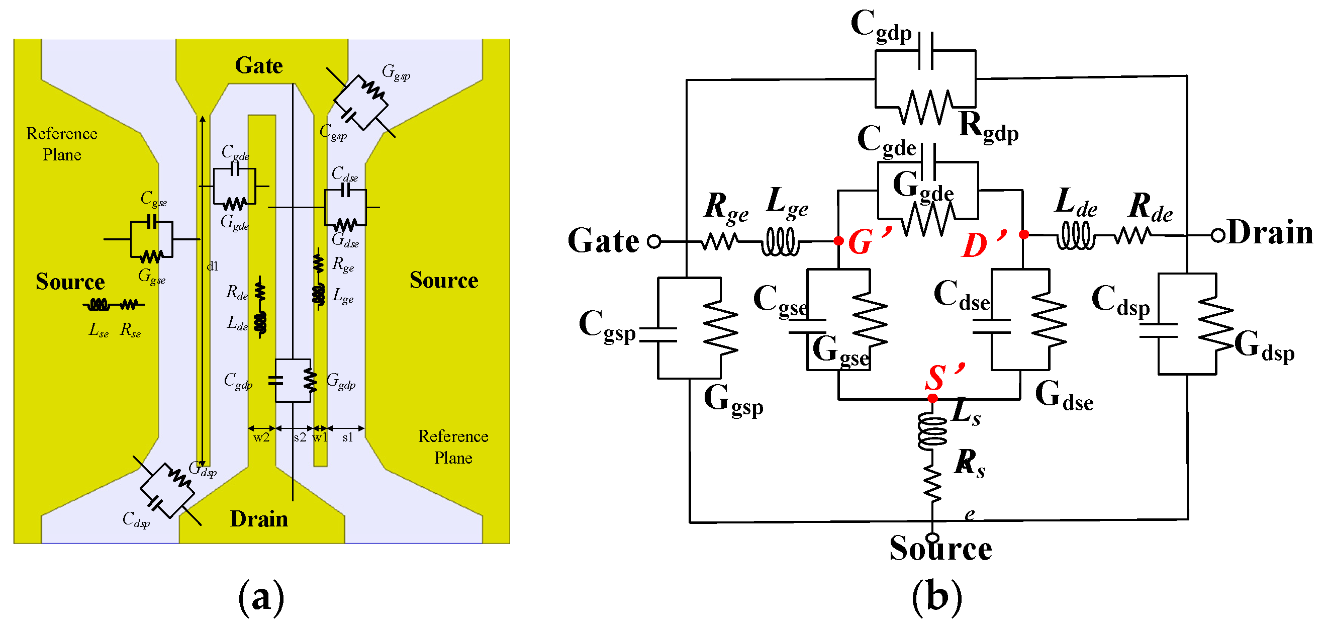
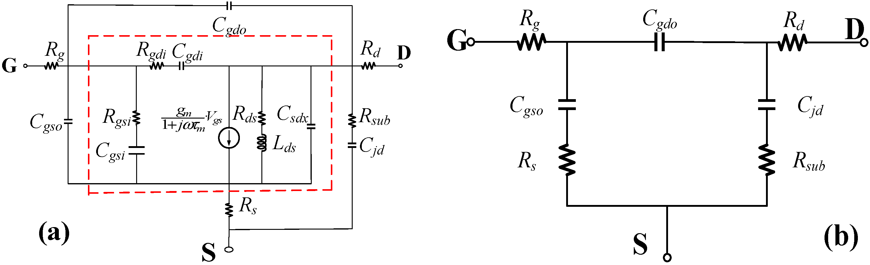
2.1. Device Structure and Equivalent Circuit Model

The 3D schematic view of the device structure for the vertically stacked GAA NSFET is shown in Figure 1a–c, depicting the 2D cross-section views along the channel and gate direction. The physical gate length Lg is 15 nm. Three nanosheets with ellipse cross-section are vertically stacked. The width and height of each nanosheet are separately 20 nm and 5 nm. The gate oxide is composed of SiO2 and HfO2 and the equivalent oxide thickness is 0.68 nm. The spacer is composed of 4.2 nm SiO2 and 1.6 nm HfO2. The doping of the channel and source/drain are 1 × 1015 cm−3 and 1 × 1021 cm−3, respectively. TiN with aa work function of 4.37 eV is adopted as the gate metal. Figure 2 shows the adopted two-finger coplanar GSG PAD layout to de-embed the impact of the test structure and the compounding equivalent circuit model. Each parasitic parameter from the layout is also marked out. Here, (Cgde, Ggde), (Cgse, Ggse) and (Cdse, Gdse) are the interconnection parasitic capacitance–conductance pairs between PAD electrodes. (Rge, Lge), (Rde, Lde) and (Rse, Lse) represent the parasitic resistance–inductance pair of PAD electrodes. (Cgdp, Ggdp), (Cgsp, Ggsp) and (Cdsp, Gdsp) are interconnection capacitance–conductance pairs between PAD electrodes.
Figure 3 shows the proposed improved small-signal equivalent circuit model of intrinsic GAAFET. Cgdo and Cgso are the capacitance between the gate and source/drain. Rg, Rs, Rd and Rsub are separately the resistance of the gate, source, drain and substrate. Cjd is the capacitance between the drain and substrate. Cgsi and Cgdi are the capacitance between the source/drain overlap and gate region. Rgsi and Rgdi are the resistance of the source and drain overlap region. Rds and Lds are the channel’s resistance and inductance. τm characterizes the transmission delay between the source and drain. Csdx characterizes the DIBL effect, and gm is the transconductance.

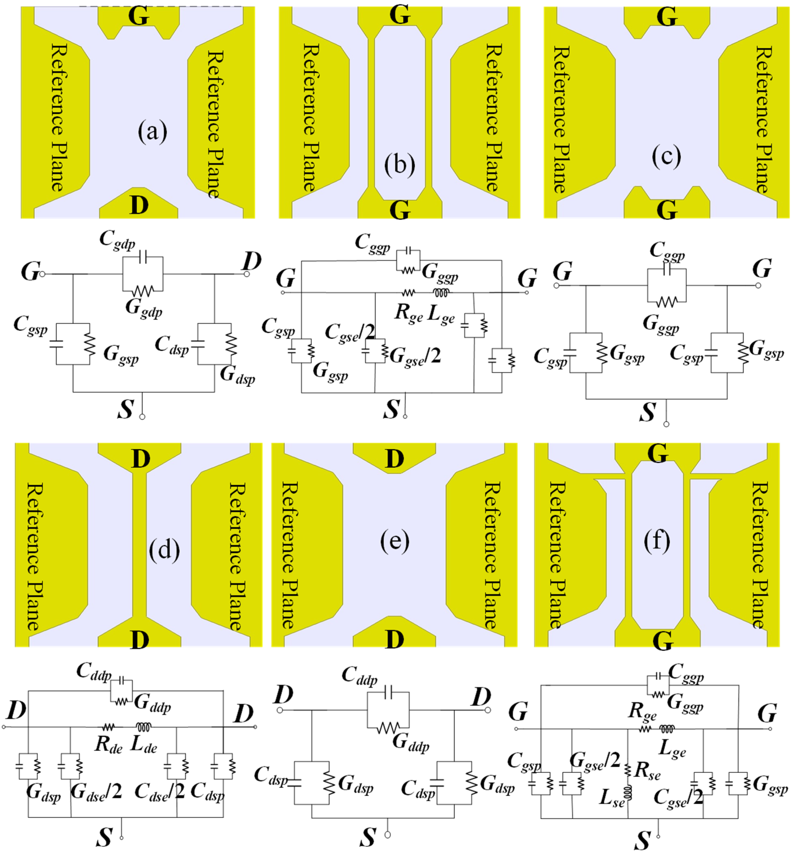
2.2. Extrinsic Layout Test Structures and Parameter Extraction Algorithm

As shown in Figure 2b, 18 parasitic elements are contained in the extrinsic GSG layout parasitic circuit. It is unrealistic to extract many parasitic parameters by directly fitting measured or simulated S (or Y)-parameters. Thus, a kind of multi-step extraction method has been proposed [10]. However, because the parasitic parameters are sensitive to the layout structure, two kinds of short structures may not match expectations when performing the fourth and fifth steps. Here, we propose an improved multi-step test structure method to better characterize the circuit performance.
First, similar to the conventional method in [18,19], the gate and drain electrodes are removed, and the PAD of the source, gate and drain is simulated to extract the coupling parasitic capacitance and conductance between PADs. The layout and corresponding sub-circuit model are shown in Figure 4a. The Y-matrix of such PADs structure is as follows:
Y P A D = ( G g s p + j ω C g s p + G g d p + j ω C g d p G g d p j ω C g d p G g d p j ω C g d p G d s p + j ω C d s p + G g d p + j ω C g d p )
Thus, Ggdp, Ggsp and Gdsp can be obtained from the real part of Ypad,12, Ypad,11 and Ypad,22, and Cgdp, Cgsp and Cdsp are the slope of the imaginary part of Ypad,12, Ypad,11 and Ypad,22 verses ω, as depicted below.
G g d p = R e ( Y p a d , 12 )
G g s p = R e ( Y p a d , 11 ) R e ( Y p a d , 12 )
G d s p = R e ( Y p a d , 22 ) R e ( Y p a d , 12 )
C g d p = I m ( Y p a d , 12 ) / ω
C g s p = [ I m ( Y p a d , 11 ) I m ( Y p a d , 12 ) ] / ω
C d s p = [ I m ( Y p a d , 22 ) I m ( Y p a d , 12 ) ] / ω
In the second step, the THRU1 structure is introduced to extract Rge and Lge. The lower half of the drain electrode is removed and the upper half is mirrored to the lower half. Then, the gate electrode is extended to connect the lower PAD, as shown in Figure 4b. Based on such THUI1 structure, the THRU1_PAD structure will be obtained when the gate electrode is removed and the corresponding sub-circuit is depicted, as seen in Figure 4c. After de-embedding the THRU1_PAD from THRU1, the admittance matrix of the gate electrode YGATE = YTHU1YTHU1_PAD is calculated as:
Y G A T E = ( ( G g s e + j ω C g s e ) / 2 + ( R g e + j ω L g e ) 1 ( G g s e + j ω C g s e ) / 2 + ( R g e + j ω L g e ) 1 ( R g e + j ω L g e ) 1 ( R g e + j ω L g e ) 1 )
Thus, similar to the extraction of Ggdp, Ggsp, Gdsp, Cgdp, Cgsp and Cdsp in Equations (2)–(7), the gate electrode resistance and inductance Rge and Lge can also be easily obtained.
In the third step, a kind of THRU2 structure is introduced. The upper half of the gate electrode is removed, and the lower half is mirrored to the upper half, then the drain electrode is extended to connect to the upper and lower PAD, as shown in Figure 4d. The corresponding THRU2_PAD structure is depicted in Figure 4e by removing the drain electrode in the THUR2 structure. The corresponding sub-circuits are separately depicted in Figure 4d,e. Similarly, the admittance matrix of the drain electrode YDRAIN = YTHU2YTHU2_PAD is written as:
Y D R A I N = ( ( G d s e + j ω C d s e ) / 2 + ( R d e + j ω L d e ) 1 ( R d e + j ω L d e ) 1 ( R d e + j ω L d e ) 1 ( G d s e + j ω C d s e ) / 2 + ( R d e + j ω L d e ) 1 )
So far, the drain electrode resistance Rde and inductance Lde are obtained.
In the fourth step, a kind of THRU1_SHORT is structured to extract Rse and Lse. The gate electrode is connected to the source PAD based on the THRU1 structure, as shown in Figure 4f. The Y-matrix of the source electrode YSOURCE is calculated as:
Y S O U R C E = ( 0 ( R s e + j ω L s e ) 1 ( R s e + j ω L s e ) 1 0 )
Thus, the source electrode resistance Rse and inductance Lse can be easily obtained.
In the fifth step, the entire layout test structure, as shown in Figure 2a, is simulated to obtain the remaining inter-electrode parasitic capacitance and inductance pairs (Cgde, Ggde), (Cgse, Ggse) and (Cdse, Gdse). The corresponding circuit is shown in Figure 2b. The parasitic network on the electrodes can be expressed as:
Z S E R I E S = ( ( R g e + j ω L g e ) + ( R s e + j ω L s e ) R s e + j ω L s e R s e + j ω L s e ( R d e + j ω L d e ) + ( R s e + j ω L s e ) )
The Y-matrix of the parasitic network between the electrodes can be expressed as:
Y E L C T R = ( G g s e + j ω C g s e + G g d e + C g d e ( G g d e + j ω C g d e ) ( G g d e + j ω C g d e ) G d s e + j ω C d s e + G g d e + C g d e )
Similar to extracting the parameters of the PAD structure, all parasitic capacitance and inductance pairs between the electrodes can be extracted here. HFSS simulation is then performed to obtain the high-frequency characteristics of the designed test structure in Figure 2 and Figure 4, and the frequency range is up to 300GHz. Then, all the model parameters related with GSG PAD can be extracted based on Equations (1)–(12).

2.3. Improved Extraction Method of Intrinsic Device Equivalent Circuit

As depicted in Figure 3a, the equivalent circuit of the intrinsic device includes 16 circuit elements. In our previous work [5], a two-step method has been proposed to extract intrinsic parameters based on the ON-state and OFF-state. However, gate resistance Rg is ignored, which is very important for the impedance matching and thermal noise of the gate metal [17]. Here, an improved extraction method including gate resistance Rg for intrinsic devices is proposed in this work.
When the device is biased at the OFF-state (Vgs ≤ 0, Vds = 0), the equivalent circuit of the intrinsic device will be reduced as shown in Figure 3b. Thus, Y-parameters Y 11 o of the OFF-state equivalent circuit in Figure 3b can be calculated as follows:
R e [ Y 11 o ] = ( N 10 ω 2 + N 11 ω 4 + N 12 ω 6 ) / ( 1 + M 11 ω 2 + M 12 ω 4 + M 13 ω 6 )
R e [ Y 12 o ] = ( N 20 ω 2 + N 21 ω 4 + N 22 ω 6 ) / ( 1 + M 11 ω 2 + M 12 ω 4 + M 13 ω 6 )
I m [ Y 12 o ] = ( N 30 ω + N 31 ω 3 + N 32 ω 5 ) / ( 1 + M 11 ω 2 + M 12 ω 4 + M 13 ω 6 )
R e [ Y 22 o ] = ( N 40 ω 2 + N 41 ω 4 + N 42 ω 6 ) / ( 1 + M 11 ω 2 + M 12 ω 4 + M 13 ω 6 )
I m [ Y 22 o ] = ( N 50 ω + N 51 ω 3 + N 52 ω 5 ) / ( 1 + M 11 ω 2 + M 12 ω 4 + M 13 ω 6 )
The coefficients Nij and Mij are functions of model parameters in Figure 3b, where the coefficients N10N50 in the numerator are shown as follows:
N 10 = C g d o 2 R d + C g s o 2 R s + R g ( C g d o + C g d o ) 2
N 20 = C g d o 2 ( R d + R g ) + C g d o ( C g s o R g + C j d R d )
N 30 = C g d o
N 40 = C g d o 2 ( R d + R g ) + C j d 2 ( R d + R s u b ) + 2 C g d o C j d R d
N 50 = C g d o + C j d
Since the source and drain are symmetrical, there exists Cgdo = Cgso and Rs = Rd. Thus, the bias-independent parameters (Cgso, Cgdo, Rs, Rd, Rg, Cjd, Rsub) can be directly obtained by grouping Equations (18)–(22), as shown below:
C g d o = C g s o = N 30
R d = R s = ( N 10 2 N 20 ) / ( 2 N 30 2 2 N 50 N 30 )
R g = ( 2 N 20 N 30 N 10 N 50 ) / [ 4 N 30 2 ( N 30 N 50 ) ]
C j d = N 50 N 30
R s u b = [ N 40 ( 2 C g d o + C j d ) C j d R d C g d o 2 ( R d + R g ) ] / C j d 2
After removing the bias-independent parameter in Figure 3b, the Y-parameter of the equivalent circuit within the redline in Figure 3a can be obtained as:
I m [ Y 11 i + Y 12 i ] = K 10 ω / ( 1 + K 11 ω 2 )   ( where   K 10 = C g s i )
R e [ Y 11 i + Y 12 i ] = K 20 ω 2 / ( 1 + K 11 ω 2 ) ( where   K 20 = C g s i 2 R g s i )
I m [ Y 12 ] = K 30 ω / ( 1 + K 31 ω 2 )   ( where   K 30 = C g d i )
R e [ Y 12 ] = K 40 ω 2 / ( 1 + K 31 ω 2 )   ( where   K 40 = C g d i 2 R g d i )
I m [ Y 21 i Y 12 i ] = K 50 ω / ( 1 + K 51 ω 2 )   ( where   K 50 = g m τ m )
I m [ Y 12 i + Y 22 i ] = ( K 70 ω + K 71 ω 3 ) / ( 1 + K 72 ω 2 )     ( where   K 70 = C s d x L d s / R d s 2 )
1 / R e [ Y 12 i + Y 22 i ] = K 80 + K 90 ω 2   ( where   K 80 = R d s , K 90 = L d s 2 / R d s )
Then, the bias-dependent parameters (Cgsi, Cgdi, Rgsi, Rgdi, τm, gm, Rds, Lds, Csdx) can be directly obtained by grouping Equations (28)–(34), as shown below:
C g s i = K 10 C g d i = K 30
R g s i = K 20 / K 10 2                                                                 R g d i = K 40 / K 30 2
τ m = K 50 / K 60                                                                   g m = K 60
R d s = K 80                                                                                           L d s = K 80 K 90
C s d x = N 70 + K 80 K 90 / K 80 2
So far, the model parameters for the intrinsic circuit have been analytically extracted, once the coefficients N10N50 and K10K90 are accurate.

3. Result and Discussion

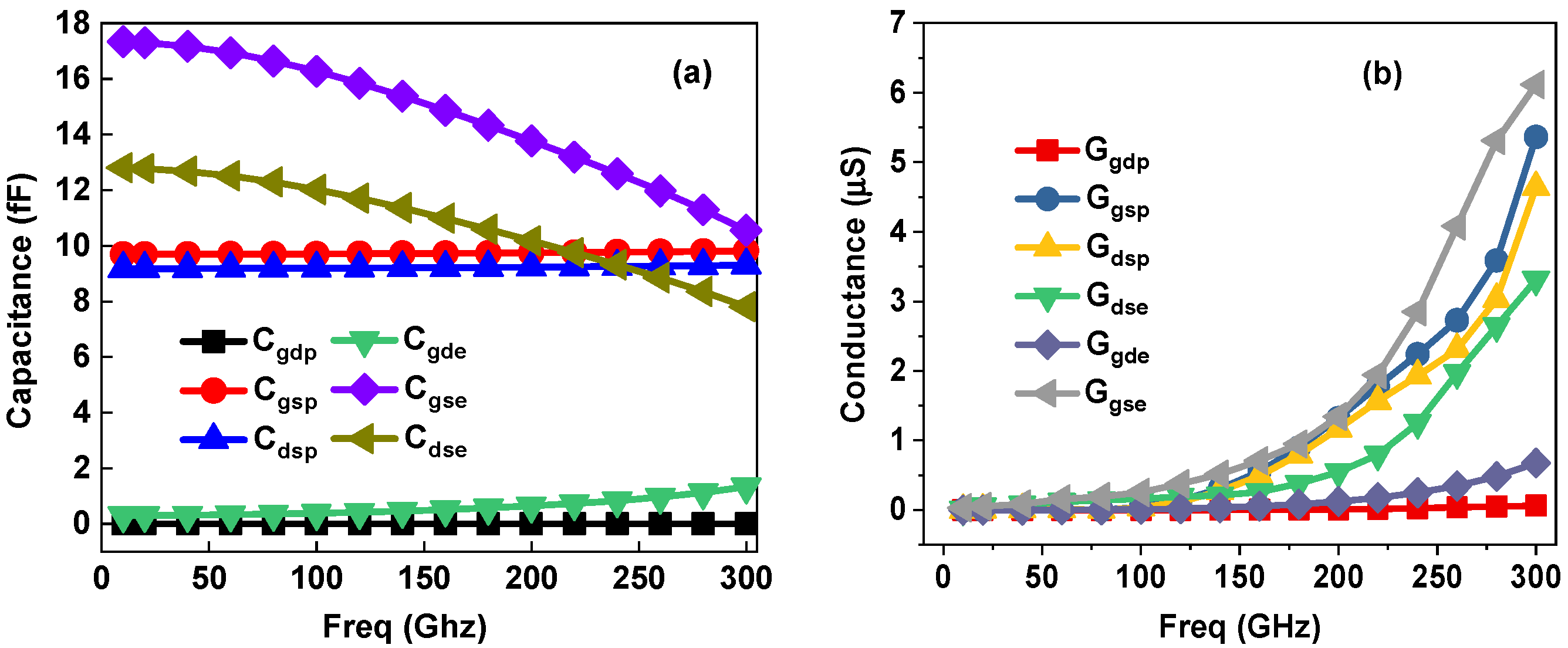
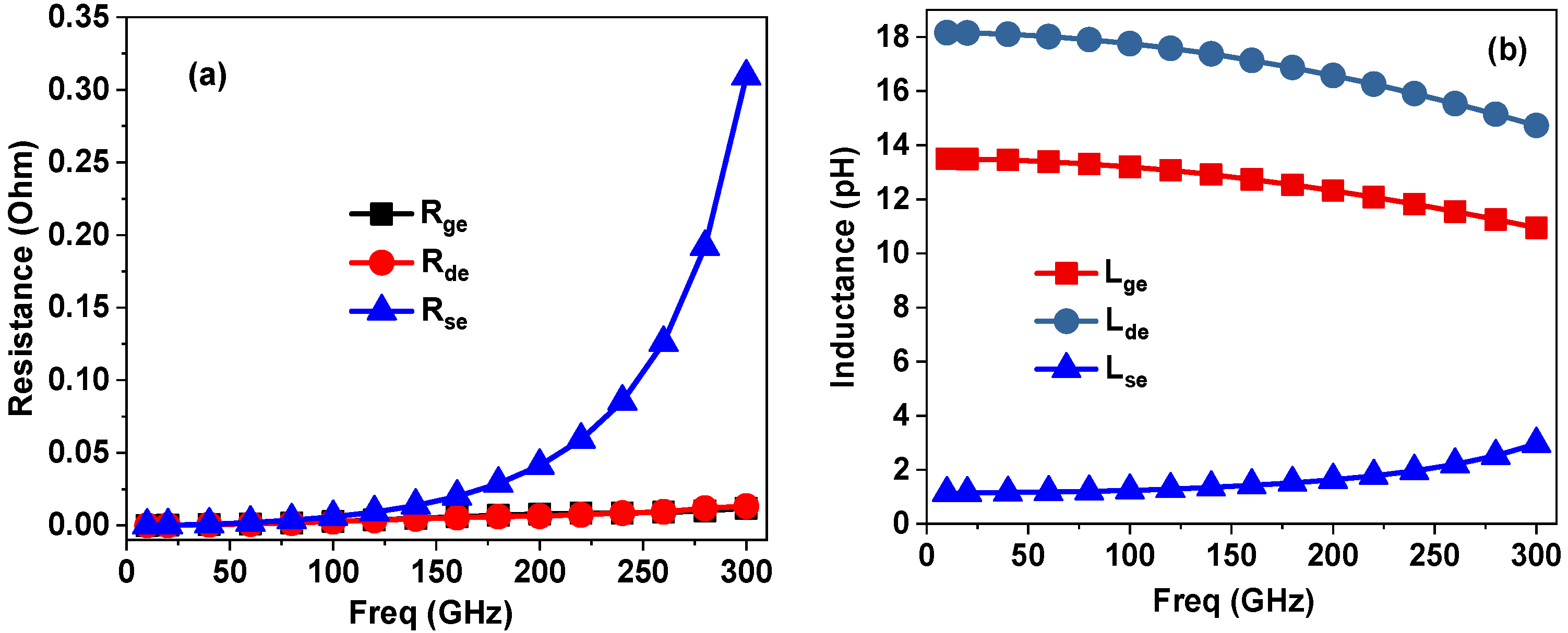
3.1. Validation of Extraction Method for Extrinsic Layout

After accurately extracting the parasitic parameters of the extrinsic GSG test layout, the full-wave EM simulation in HFSS is compared with the ADS simulation using the equivalent circuit. The accuracy of the proposed improved extrinsic layout extraction method is confirmed over 10 MHz–300 GHz. Figure 5 shows the comparison between simulated and modeled S-parameters for the standard OPEN test structure in Figure 2a. The S-parameters obtained by the full-wave EM simulation show an excellent agreement with the extracted equivalent circuit over a wide bandwidth, which confirms the accuracy of the proposed improved extraction method.
Figure 6a shows the extracted inter-electrode and inter-pad capacitors. Consistent with [18,19], Cgdp and Cgde are much smaller than the other capacitances because of the large space and small co-planar capacitance between the gate and drain electrode [20,21]. Moreover, Cgse and Cdse decrease with increasing frequency, due to the neglection of the inductance of the source, gate and drain PADs [22]. Figure 6b shows the variation of Ggsp, Gdsp, Ggdp, Ggse, Gdse and Ggde as functions of frequencies. For the substrate capacitance and inductance, there is a relation of G (ω)/C (ω) = ωtanδ (where δ represent dielectric constant), and the inductances are basically proportional to its corresponding capacitances [23]. The parasitic resistance–inductance pairs (Rge, Lge), (Rde, Lde) and (Rse, Lse) between the source and gate electrodes are shown in Figure 7, respectively. Due to the current crowding phenomenon and the skin effect, the source resistance Rse rises rapidly as the frequency enters the mmW band. Due to the skin effect, Lge and Lde gradually decrease as the frequency increases. The conductor inductance of the microstrip line is inversely proportional to its width, while the width of the source electrode is wider than the other electrodes, which leads to a smaller source electrode inductance Lse.

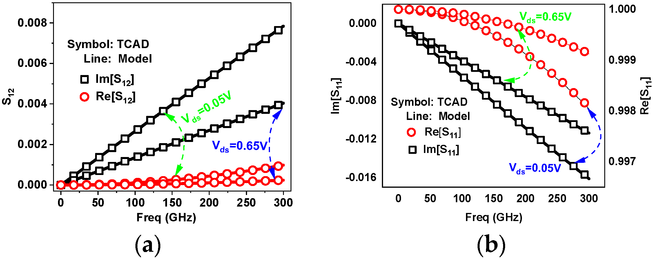
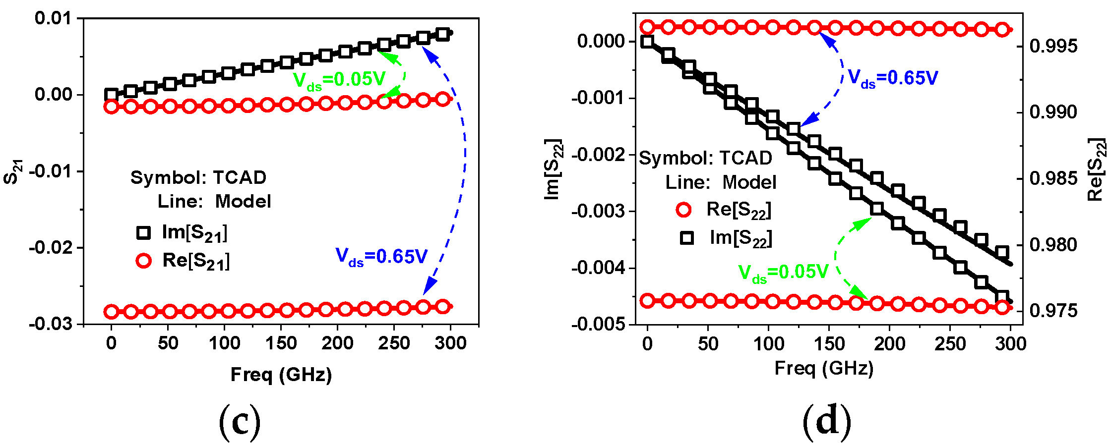
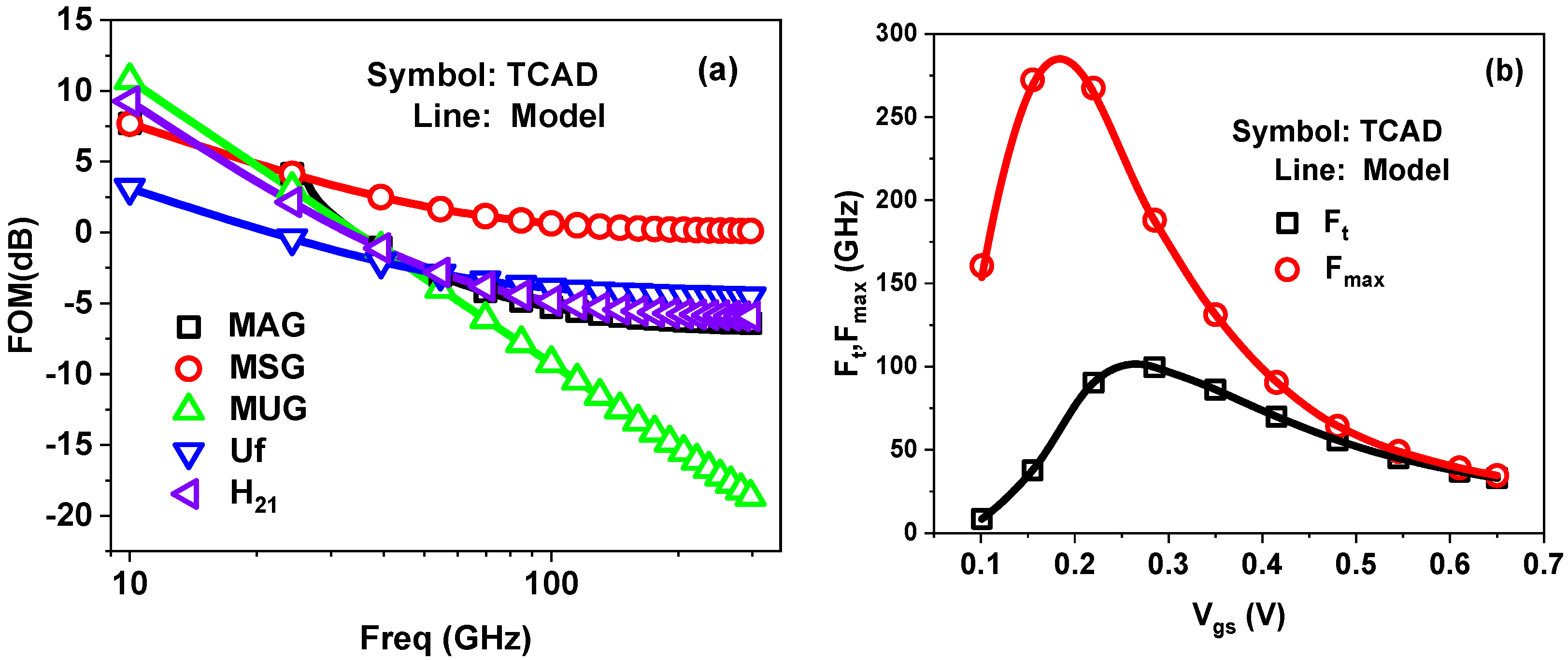
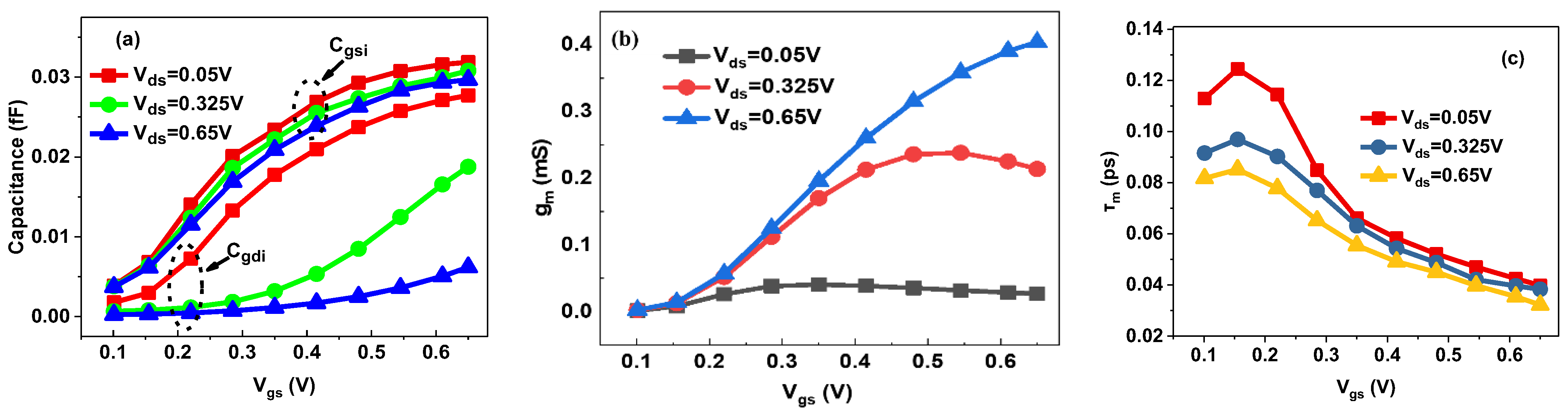
3.2. Validation of Extraction Method for Intrinsic Device

Sentaurus TCAD is adopted to obtain the high-frequency characteristics of intrinsic NSFET under the ON-state. The critical physical model used in the device simulation includes the drift-diffusion model, density-gradient model, Philips unified mobility model, interface mobility degradation model, velocity saturation and doping-dependent SRH recombination. The simulated high-frequency S-parameters are used to verify the accuracy and feasibility of the small-signal circuit and parameter extraction method. With the help of mathematical fitting software such as MATLAB, the lowest order terms Ni0 and Ki0 in Equations (12)–(16) and (22)–(29) can be accurately determined. As for the 3 nm nanosheet transistor in the proposed OFF-state bias (Vgs = −0.65 V, Vds = 0 V), the fitting results of Ni0 and the corresponding confidence interval are shown in Table 1. The narrow confidence interval verifies the accuracy of Ni0. According to Equations (17)−(21), the bias-independent parameters under such OFF-state are separately extracted as: Cgso = Cgdo = 1.466 × 10⁻¹⁷ F, Rs = Rd = 837.16 Ω, Rg = 17.29 Ω, Cjd = 9.9 × 10⁻¹⁹ F and Rsub = 9943.3 Ω. The comparison between the TCAD device simulation in Sentaurus and equivalent circuit simulation in ADS is shown in Figure 8, from which a good agreement exists over 10 MHz–300 GHz.
Similar to the above OFF-state, the coefficients Ki0 for the ON-state can also be accurately determined. For example, the fitting results for the linear region (Vgs = 0.65 V, Vds = 0.05 V) are shown in Table 2. The reliability of Ki0 can also be proved by the corresponding narrow confidence interval. According to Equations (30)–(34), the bias-independent intrinsic model parameters under such ON-state are calculated as: Cgsi = 2.968 × 10⁻¹⁷ F, Cgdi = 2.77 × 10⁻¹⁷ F, Rgsi = 916.33 Ω, Rgdi = 1331.3 Ω, τm = 32.2 fs, gm=2.71 × 10⁻⁵ S, Csdx = 1.90 × 10⁻¹⁸ F and Rds = 2357 Ω. S-parameter comparison between the Sentaurus device simulation and ADS equivalent circuit simulation under a linear region (Vgs = 0.65 V, Vds = 0.05 V) and saturation region (Vgs = 0.65 V, Vds = 0.65 V) is depicted in Figure 9. Excellent agreement is obtained over the entire frequency. The maximum error in the linear region and saturation region are 0.2504% and 2.689%, which confirms the accuracy of the proposed extraction method.
Figure 10a shows the comparison between simulated and modeled maximum available gain (MAG), maximum stable gain (MSG), Mason’s unilateral gain (MUG), unilateral figure of merit (Uf) and H21. As expected, ADS-modeled data agree well with the Sentaurus simulated one over the whole frequency range. The extracted cutoff frequency Ft and maximum oscillation frequency Fmax under different biases shown in Figure 10b. As expected, Ft and Fmax increase first and then decrease with increasing Vgs. Excellent agreement between the simulated and modeled RF figures of merit (FOM) proves that the extracted small-signal equivalent circuit can effectively predict the RF response of the device up to 300 GHz. Subsequently, the bias dependence of intrinsic model parameters is discussed. Figure 11 shows the variation of extracted critical model parameters as a function of Vgs. Cgsi/Cgdi gradually increases as Vgs increases, and then becomes flat when Vgs is large enough, which is consistent with the typical C-V curve of MOS capacitor. Moreover, Cgdi is smaller than Cgsi under the same Vds, and the difference between two capacitances increases with increasing Vds, especially in the saturation region, which is the result of the thinner depletion layer near the drain region. gm sharply increases when the transistor operates in the saturation region, and the increasing trend slows down once the transistor enters the linear region, due to the carrier velocity saturation effect under high electric field. τm is found to first increase and then decrease with increasing Vgs. Similar to the planar MOSFET, τm can be expressed as:
τ m L G 2 μ n ( V g s V t h )
In the above formula, the mobility μn decreases with increasing Vgs. These two items in the denominator contribute a competitive relationship, which causes τm to increase first and then decrease.

4. Conclusions

In this paper, an improved RF small-signal equivalent circuit model and corresponding parameter extraction method is proposed for GAAFET at 3 nm node. The equivalent circuit contains both the extrinsic GSG test layout and intrinsic device. The parasitic parameters of the GSG test layout are first obtained by an improved five-step method. The model parameters of the intrinsic GAAFET are analytically extracted with the help of nonlinear rational function fitting. The validity of the proposed small-signal equivalent circuit model and the corresponding extraction method have been demonstrated, through excellent agreement between TCAD/HFSS 3D full-wave simulation and equivalent circuit frequency response up to 300 GHz. The error is lower than 2.69% for intrinsic devices, and lower than 0.89% for the extrinsic GSG test layout in the whole frequency range. Moreover, an obvious influence of WFV is found on the variation of critical model parameters, especially under the condition of smaller gate grain size.

Author Contributions

Conceptualization and methodology Z.L.; validation X.L.; writing—original draft preparation, H.G.; writing—review and editing, Y.S. (Yabin Sun); visualization, Y.L.; supervision, Y.S. (Yanling Shi); formal analysis and data curation, S.H. All authors have read and agreed to the published version of the manuscript.

Funding

This research was funded by the National Natural Science Foundation of China, grant number 61974056; Science Foundation of Shanghai, grant number 19ZR1471300; Shanghai Science and Technology Innovation Action Plan, grant number 19511131900; and Shanghai Science and Technology Explorer Plan, grant number 21TS1401700.

Data Availability Statement

The datasets generated during and/or analysis during the current study are available from the corresponding author on reasonable request.

Conflicts of Interest

The authors declare no conflict of interest.

References

  1. D’Agostino, F.; Quercia, D. Short-Channel Effects in MOSFETs. In Integrated Nanoelectronics. NanoScience and Technology; Springer: New Delhi, India, 2016. [Google Scholar] [CrossRef]
  2. Lee, H.J.; Rami, S.; Ravikumar, S.; Neeli, V.; Phoa, K.; Sell, B.; Zhang, Y. Intel 22nm FinFET (22FFL) Process Technology for RF and mmWave Applications and Circuit Design Optimization for FinFET Technology. In Proceedings of the 2018 IEEE International Electron Devices Meeting (IEDM), San Francisco, CA, USA, 1–5 December 2018. [Google Scholar]
  3. Loubet, N.; Hook, T.; Montanini, P.; Yeung, C.W.; Kanakasabapathy, S.; Guillom, M.; Yamashita, T.; Zhang, J.; Miao, X.; Wang, J.; et al. Stacked nanosheet gate-all-around transistor to enable scaling beyond FinFET. In Proceedings of the 2017 Symposium on VLSI Technology, Kyoto, Japan, 5–8 June 2017. [Google Scholar]
  4. Heydari, B.; Bohsali, M.; Adabi, E.; Niknejad, A.M. Millimeter-wave devices and circuit blocks up to 104 GHz in 90 nm CMOS. IEEE J. Solid-State Circuits 2007, 42, 2893–2903. [Google Scholar] [CrossRef] [Green Version]
  5. Qin, M.; Sun, Y.; Li, X.; Shi, Y. Analytical parameter extraction for small-signal equivalent Circuit of 3D FinFET into Sub-THz range. IEEE Access 2018, 6, 19752–19761. [Google Scholar] [CrossRef]
  6. Sun, Y.; Gao, H.; Li, X.; Yang, X.; Liu, Z.; Liu, Y.; Li, X.; Shi, Y. Impact of process fluctuations on RF small-signal parameter of gate-all-around nanosheet transistor beyond 3 nm node. IEEE Trans. Electron. Devices 2021, 69, 31–38. [Google Scholar] [CrossRef]
  7. Zhang, W.; Yin, S.; Hu, W.; Wang, Y. Novel Physics-based small-signal modeling and characterization for advanced RF bulk FinFETs. IEEE Trans. Electron. Devices 2021, 68, 2160–2166. [Google Scholar] [CrossRef]
  8. Koolen, M.; Geelen, J.; Versleijen, M. An improved de-embedding technique for on-wafer high-frequency characterization. In Proceedings of the 1991 Bipolar Circuits and Technology Meeting, Minneapolis, MN, USA, 9–10 September 1991. [Google Scholar]
  9. Crupi, G.; Schreurs, D.M.-P.; Caddemi, A. Accurate silicon dummy structure model for nonlinear microwave FinFET modeling. Microelectron. J. 2010, 41, 574–578. [Google Scholar] [CrossRef]
  10. Karisan, Y.; Caglayan, C.; Trichopoulos, G.C.; Sertel, K. Lumped-element equivalent-circuit modeling of millimeter-wave HEMT parasitics through full-wave electromagnetic analysis. IEEE Trans. Microw. Theory Tech. 2016, 64, 1419–1430. [Google Scholar] [CrossRef]
  11. Liu, Z.; Huang, X.; Lee, F.C.; Li, Q. Package parasitic inductance extraction and simulation model development for the high-voltage cascode GaN HEMT. IEEE Trans. Power Electron. 2013, 29, 1977–1985. [Google Scholar] [CrossRef]
  12. Karisan, Y.; Sertel, K. Extraction of parasitics in GaN HEMTs via full-wave electromagnetic modeling. In Proceedings of the NAECON 2014-IEEE National Aerospace and Electronics Conference, Dayton, OH, USA, 24–27 June 2014; pp. 306–307. [Google Scholar]
  13. Jung, J.-H.; Lee, J.-H. Extraction of substrate resistance in bulk FinFETs through RF modeling. IEEE Microw. Wirel. Compon. Lett. 2007, 17, 358–360. [Google Scholar] [CrossRef]
  14. Deschrijver, D.; Avolio, G.; Schreurs, D.; Dhaene, T.; Crupi, G.; Knockaert, L. Microwave small-signal modelling of FinFETs using multi-parameter rational fitting method. Electron. Lett. 2011, 47, 1084–1086. [Google Scholar] [CrossRef] [Green Version]
  15. Chalkiadaki, M.-A.; Enz, C.C. RF Small-signal and noise modeling including parameter extraction of nanoscale MOSFET from weak to strong inversion. IEEE Trans. Microw. Theory Tech. 2015, 63, 2173–2184. [Google Scholar] [CrossRef]
  16. Crupi, G.; Schreurs, D.; Parvais, B.; Caddemi, A.; Mercha, A.; Decoutere, S. Scalable and multibias high frequency modeling of multi-fin FETs. Solid-State Electron. 2006, 50, 1780–1786. [Google Scholar] [CrossRef]
  17. Kang, I.M.; Shin, H. Non-quasi-static small-signal modeling and analytical parameter extraction of SOI FinFETs. IEEE Trans. Nanotechnol. 2006, 5, 205–210. [Google Scholar] [CrossRef]
  18. Zhu, G.; Chang, C.; Xu, Y.; Zhang, Z.; Al-saman, A.A.; Lin, F. A millimeter-wave scalable small-signal modeling approach based on FW-EM for AlGaNGaN HEMT up to 110_GHz. Microw. Opt. Technol. Lett. 2020, 63, 2145–2152. [Google Scholar] [CrossRef]
  19. Jia, Y.; Xu, Y.; Xu, R.; Li, Y. An accurate parasitic parameters extraction method based on FW-EM for AlGaNGaN HEMT up to 110 GHz. Int. J. Numer. Model. Electron. Netw. Devices Fields 2017, 31, 2270. [Google Scholar] [CrossRef]
  20. Choe, K.; An, T.; Kim, S. Accurate fringe capacitance model considering RSD and metal contact for realistic FinFETs and circuit performance simulation. In Proceedings of the 2014 International Conference on Simulation of Semiconductor Processes and Devices (SISPAD), Yokohama, Japan, 9–11 September 2014; pp. 29–32. [Google Scholar]
  21. Chen, Y.; Zhang, Y.; Xu, Y.; Sun, Y.; Cheng, W.; Lu, H.; Xiao, F.; Xu, R. Investigation of Terahertz 3D EM Simulation on Device Modeling and A New InP HBT Dispersive Inter-Electrode Impedance Extraction Method. IEEE Access 2018, 6, 45772–45781. [Google Scholar] [CrossRef]
  22. Zheng, J.; Hahm, Y.-C.; Tripathi, V.; Weisshaar, A. CAD-oriented equivalent-circuit modeling of on-chip interconnects on lossy silicon substrate. IEEE Trans. Microw. Theory Tech. 2000, 48, 1443–1451. [Google Scholar] [CrossRef] [Green Version]
  23. Tsividis, Y. Operation and Modeling of MOS Transistor; McGraw-Hill: New York, NY, USA, 1999. [Google Scholar]
Figure 1. Intrinsic 3 nm nanosheet GAAFET. (a) 3D schematic and (b) 2D cross-section along AA’ direction and (c) BB’ direction.
Processes 10 01198 g001
Figure 2. (a) The adopted two-finger coplanar GSG PAD layout and (b) the equivalent circuit of GSG PAD layout.
Processes 10 01198 g002
Figure 3. The equivalent circuit of intrinsic GAAFET under (a) ON-state, where the elements within the redline are bias-dependent, and (b) OFF-state, where the elements are bias-independent.
Processes 10 01198 g003
Figure 4. Improved test structure and corresponding sub-circuit model for extrinsic G parasitic circuit extraction. (a) PAD; (b) THRU1; (c) THRU1_PAD; (d) THRU2; (e) THRU2_PAD; and (f) THRU1_SHORT.
Processes 10 01198 g004
Figure 5. Comparison between simulated and modeled S-parameters for the extrinsic layout OPEN structure. (a) S11, S12 and (b) S22.
Processes 10 01198 g005
Figure 6. (a) Inter-electrode equivalent capacitances and (b) inter-electrode equivalent conductance of the GSG test layout.
Processes 10 01198 g006
Figure 7. The resistance and inductance on the source and drain gate electrodes: (a) Rge, Rde and Rse; (b) Lge, Lde and Lse.
Processes 10 01198 g007
Figure 8. Comparison between simulated (symbols) and modeled S-parameters (solid lines) under OFF-state bias Vgs = −0.65 V, Vds = 0 V. (a) S11 and S22, (b) S12.
Processes 10 01198 g008
Figure 9. Comparison between TCAD-simulated and -modeled S-parameters under Vgs = 0.65 V, Vds = 0.05 V and Vgs = 0.65 V, Vds = 0.65 V. (a) S12, (b) S11, (c) S21 and (d) S22.
Processes 10 01198 g009aProcesses 10 01198 g009b
Figure 10. Comparison between simulated (symbols) and modeled (solid lines) (a) MAG, MSG, MUG, Uf and H21 under Vgs = 0.65 V, Vds = 0.65 V. (b) Ft and Fmax as a function of Vgs under Vds = 0.05 V.
Processes 10 01198 g010
Figure 11. Variation of extracted model parameters as a function of Vgs, (a) Cgsi and Cgdi, (b) gm and (c) τm.
Processes 10 01198 g011
Table 1. The fitted constant Ni0 and the corresponding confidence interval for 3 nm GAA nanosheet under Vgs = −0.65 V, Vds = 0 V.
ParametersValuesConfidence Intervals (CIs)
N10 (1 × 10⁻³¹)3.747(3.745, 3.749)
N20 (1 × 10⁻³¹)1.995(1.991, 1.998)
N30 (1 × 10⁻¹⁷)1.466(1.465, 1.467)
N40 (1 × 10⁻³¹)2.185(2.179, 2.182)
N50 (1 × 10⁻¹⁷)1.565(1.564, 1.566)
Table 2. The fitted constant Ki0 and the corresponding confidence interval under Vgs = 0.65 V, Vds = 0.05 V.
ParametersValuesConfidence Intervals (CIs)
K10 (1 × 10⁻¹⁶)0.2968(0.2968, 0.2968)
K20 (1 × 10⁻³¹)8.072(8.07, 8.075)
K30 (1 × 10⁻¹⁶)0.2772(0.2772, 0.2773)
K40 (1 × 10⁻³¹)10.23(10.23, 10.24)
K50 (1 × 10⁻¹⁸)−0.8724(–0.8726, –0.8721)
K60 (1 × 10⁻⁴)0.2706(0.2705, 0.2706)
K70 (1 × 10⁻¹⁷)–1.187(–1.188, –1.187)
K80 (1 × 10⁻³)2.357(2.357, 2.357)
K90 (1 × 10⁻²³)0.2484(0.2469, 0.2498)
Publisher’s Note: MDPI stays neutral with regard to jurisdictional claims in published maps and institutional affiliations.

