1. Introduction
With the rapid development and wide application of cloud computing and big data, higher requirements are put forward for data center network and optical interconnection technology [
1]. In recent years, the transmission rate of server access switches has tended to be higher and requires higher performance, which in turn necessitates the transmission rate of optical modules to evolve from 100 Gbps to 400 Gbps or even 800 Gbps [
2,
3]. Therefore, the design, manufacture, use and maintenance of optical modules is faced with more severe challenges [
4]. So far, there are four main packaging forms of silicon optical chips and electrical chips: monolithic integration, 2D packaging, 2.5D packaging and 3D packaging [
5]. For monolithic integration, it is difficult to fabricate a light mask because the CD (Critical Dimension) of the driver and the TIA are advanced, while optical chips do not depend on the promotion of CD. The 2D integration scheme is to mount the optical chip and the electrical chip on the PCB (printed circuit board) by bonding wire or flip-chip. With the increase of single channel bandwidth, the bonding wire bring obvious inductive parasitic effects [
6]. At the same time, because the chip edge density is limited, it is not conducive to further increasing the interconnection density. The 2.5D integration solution is a compromise for the 3D integration solution: the optical chip and the electrical chip are mounted on the passive interposer through flip-chip interconnection and input/output through a RDL (redistribution layer) and TSV (through silicon via) [
7]. Although the 2.5D integration scheme avoids the design and manufacturing difficulties caused by TSVs on the chip to a certain extent, it also inevitably introduces some other difficulties. Due to the problem of the downward optical port caused by the flip-chip, the optical coupling problem of the optical chip is greatly amplified. At the same time, compared to true 3D integration, the high-speed signal path needs to go through two bumps from the electrical chip to the interposer to the optical chip and longer RDL transmission lines, which brings signal integrity challenges. Therefore, due to the advantages of up-facing optical interface, short interconnection path and good signal quality, the research of 3D integration solution is still the most common way of achieving high bandwidth, high integration and high performance [
8].
Despite the advantages mentioned above, 3D integration still has some problems in large-scale applications. When an interposer is used as an optical chip at the same time, it is necessary to solve the problems of the RDL and TSV of the passive interposer and the co-design and manufacturing of photonic integrated circuits. Different from the active electric interposer, the active optical interposer also needs to solve the problem of optical coupling [
9]. There are two main forms of optical coupling: grating coupler and edge coupler [
10,
11]. Since the manufacturing process of TSV needs to go through the steps of drilling, insulating layer deposition, seed layer deposition and electroplating copper filling, it does not match the structure of grating coupler [
12,
13,
14]. For edge couplers, the cantilever structure is usually used, which will bring the problem of glue overflow. At the same time, the thickness of the fiber also affects the assembly of the interposer to the substrate. In a word, 3D optical modules oriented to data center optical interconnections need to solve the problems of high frequency characteristics of extra-short reach (XSR) Serdes transmission channels, good optical coupling loss characteristics and collaborative design and manufacturing [
15,
16].
Ideal high frequency characteristics and extremely low optical coupling loss have been designed and tested [
17]. In this paper, the fabrication analysis and assembly verification of the three-dimensional optical transceiver module was completed. Different active interposer processes with integrated edge couplers and RDL-TSV-RDL structures were discussed, manufactured, analyzed and evaluated. The problem of the co-fabrication of TSV and edge coupler and risk point control of 3D assembly were solved through a3D co-packaging scheme of the integrated transceiver module which was preliminarily verified, providing a good research foundation for further research and market application.
The following is the structure of the paper:
Section 1 is the overview of optical interconnection in data centers and the evolution and advantages and disadvantages of optical integration solutions.
Section 2 is the integration scheme of a 3D optical transceiver module. The comparison of the process scheme of the adapter with integrated edge coupler and RDL-TSV-RDL structure and the introduction of the process flow adopted are shown in
Section 3.
Section 4 is concerned with the design and manufacture of packaging substrate. The assembly, testing and results of the 3D optical module are also presented in
Section 4.
Section 5 delivers the conclusions.
2. Structure Design of 3D Optical Transceiver Module
The integrated transceiver module is usually composed of lasers, optical couplers, optical fibers, optical waveguides, optical modulators, the optical detectors and other optical chips; driver, the CDR (clock and data recovery), the TIA (trans-impedance amplifier), the DSP (digital signal processing) and other electrical chips; interconnected lines, holes, solder bumps, TSVs and other connection channels [
18].
Due to the difficulty of realizing silicon-based light source and the process compatibility of an on-chip integrated III-V light source, the light source is generally used as a discrete optical device to achieve light incidence through fiber and coupler [
19,
20]. Except for the light source, the other optical chips can be integrated as a single chip. Due to the larger size of the optical chip and the independence of the advanced CD, although the electrical chip has higher integration density, smaller size and advanced CD, it is more conducive to the integration of the system to take the optical chip as the interposer to undertake the interconnection function.
A general diagram of a 3D integrated optical transceiver module is shown in
Figure 1: driver, CDR, TIA and other electrical chips are inverted in the photonic integrated circuits (PICs: modulator and detector, etc.) face to face. The connections between chips and the external are transmitted through RDL, TSV and Solder ball bumps or copper pillar bumps.
Because the thickness of the thinned silicon photonic interposer is only 100 μm, the optical module needs to be placed on one side of the packaging substrate to prevent the lower cover of the standard optical fiber from coupling. Some methods can also be adopted in the packaging substrate to facilitate fiber coupling, such as substrate hollowing out.
For active silicon interposer, there are three main TSV fabrication processes, which are “TSV-first” [
21], “TSV-middle” [
22] and “TSV-last” [
23], as shown in
Figure 2.
In the “TSV-first” process, TSV is etched before the CMOS device or optical device, which has less impact on the performance of photonic device. However, polysilicon is usually selected as the filling material, resulting in poor DC and RF characteristics. In the “TSV-middle” process, TSV is etched after FEOL process and before BEOL process. Metal can be used as the filling material to achieve better RF characteristics. In the “TSV-last” process, TSV is fabricated after the CMOS device or optical device, which usually requires adding the RDL to interconnect TSVs and pins.
Currently, active silicon interposer are basically manufactured with the interaction of TSV and electrical chips, and the TSV-middle process is used as the mainstream process for manufacturing due to its better RF characteristics and higher integration level. However, no mature process flows or products have been reported for the interaction between optical chips and TSVs. Therefore, a detailed process comparison and analysis of the manufacturing process options for TSV and optical devices is presented in this paper, which provides a strong support for the future manufacturing of active photonic interposers and the integration of 3D optical co-package modules.
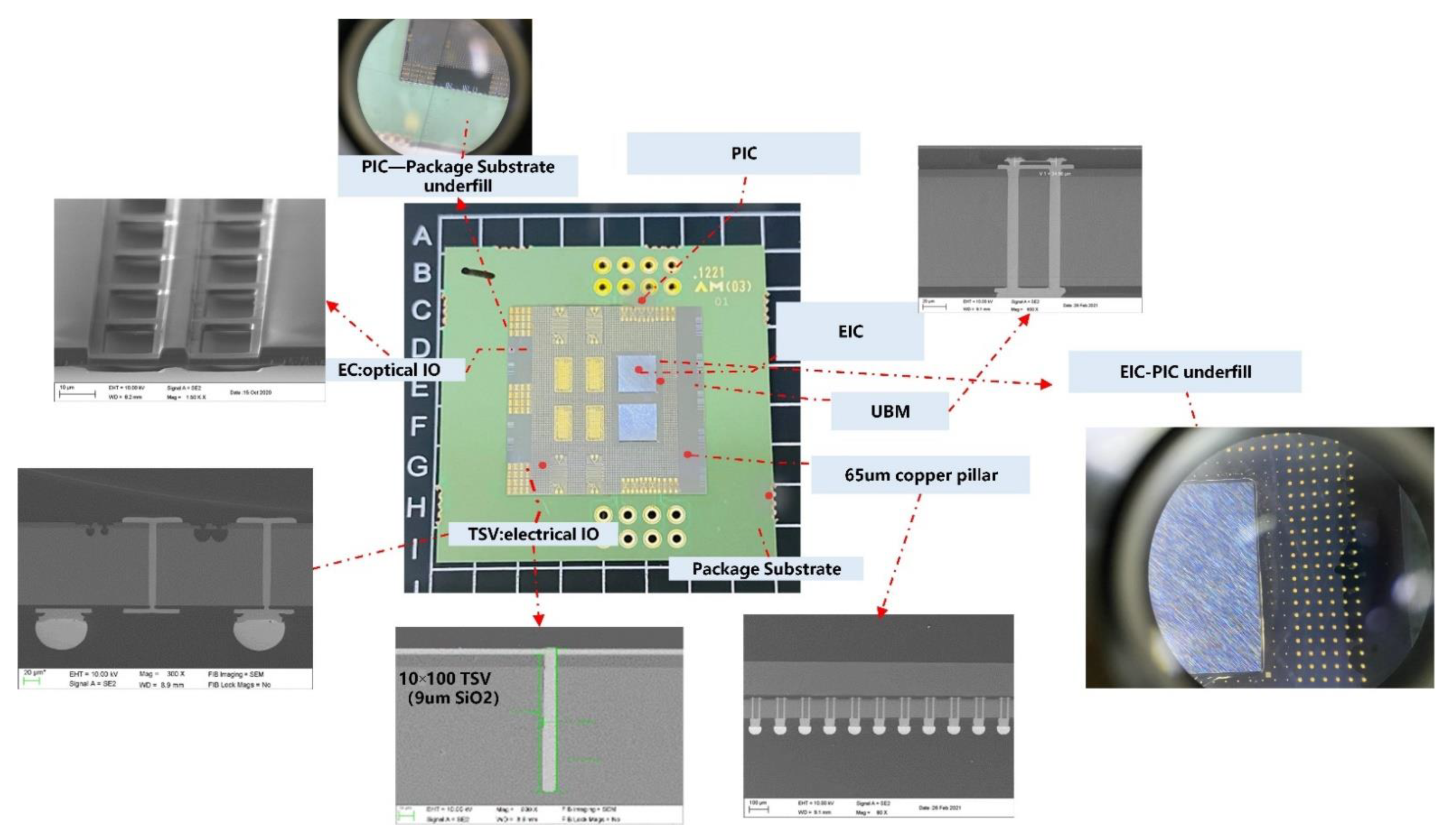
In this paper, two dummy EIC (electrical integrated circuit) chips are designed for 3D assembly. One is 4 mm × 4 mm and 200 um thickness and another is 2 mm × 4 mm. The active photonic interposer is 20 mm × 20 mm. The mask design of the electrical chip and the optical interposer chip is shown in the
Figure 3.
3. Manufacture of Active Photonic Interposer
Considering the process compatibility of edge coupler and TSV fabrication, two different schemes were considered: TSV first and then EC (Edge Coupler); EC first and then TSV. In the following, these two schemes were introduced and evaluated in detail.
The process flow diagram of different active adapter board manufacturing solutions is shown in
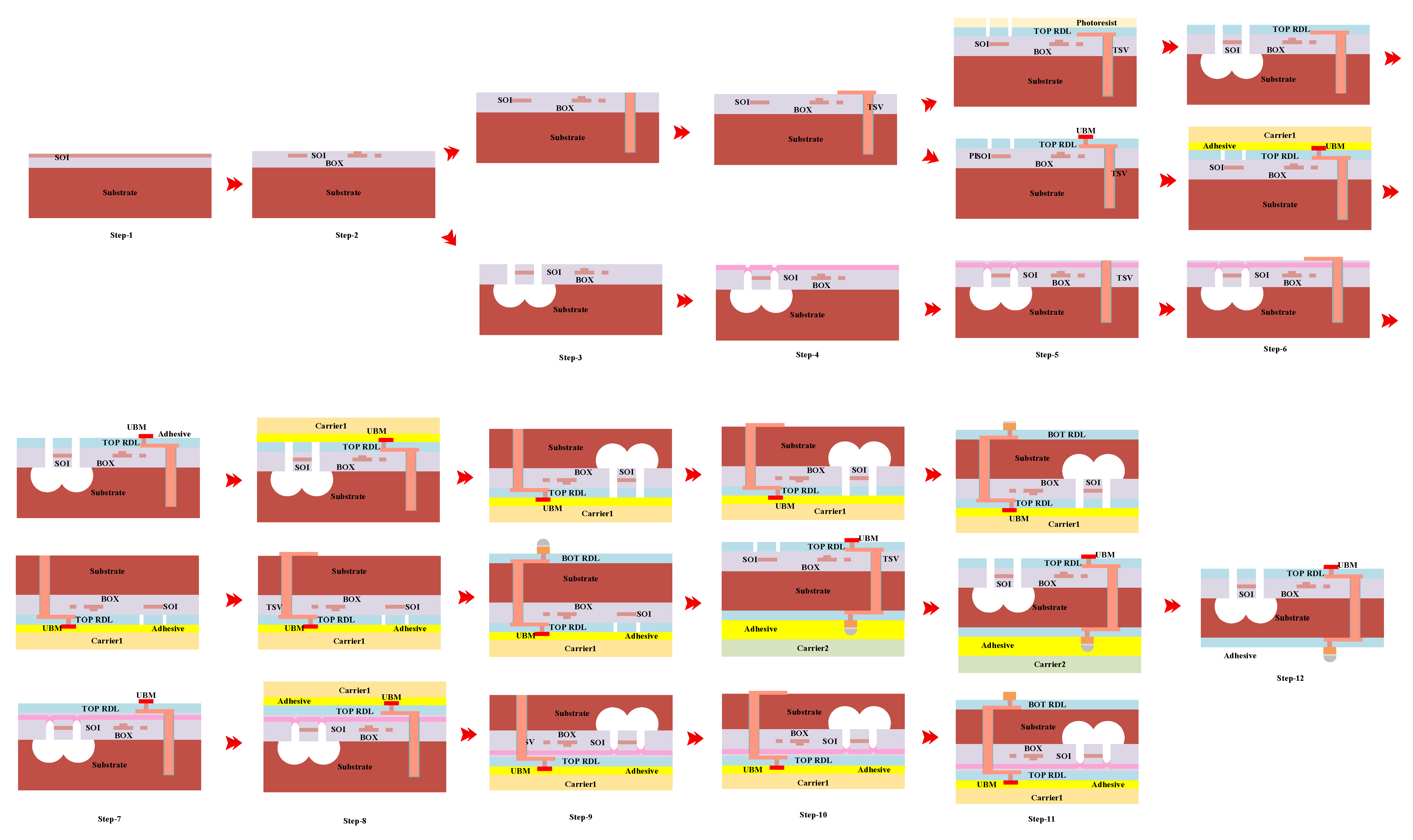
Figure 4. The process design is based on SOI (silicon on insulator) wafers. The etching of the waveguide was completed first, followed by the TSV process (etching, insulation and seed layer deposition and copper filling). Edge coupler etching and the release of silicon were conducted and then the temporary bonding above was used to further make the outcrop of TSV and to complete the RDL and copper pillar bumps (CPBS) on the backside.
However, there will be temporary bonding glue on the cavity of the edge coupler, which will inevitably affect the subsequent assembly and the performance of the edge coupler. Therefore, improved process flow methods are considered and implemented. The EC process is moved to the temporary bonding and back thinning process, which will solve the risk of bonding glue into EC cavity. After the front process of RDL and UBM (under-bump metallization) is completed, the temporary bonding above is used to further make the outcrop of TSV and to complete the RDL and copper pillar bumps (CPBS) on the backside. Similarly, temporary bonding is required to further complete edge coupler etching and the release of silicon.
To achieve blind hole etching of 10 × 100 um TSV on a wafer with
thickness of about 7 um, it is necessary to optimize the
/Si interface, for which a single step process is performed to verify the optimization, shown in
Figure 5 By using PE-TEOS process [
24],
film with target thickness of 7 um was deposited on the wafer surface. The 10 × 100 um TSV blind hole etching, side wall insulation and side wall metal deposition are realized.
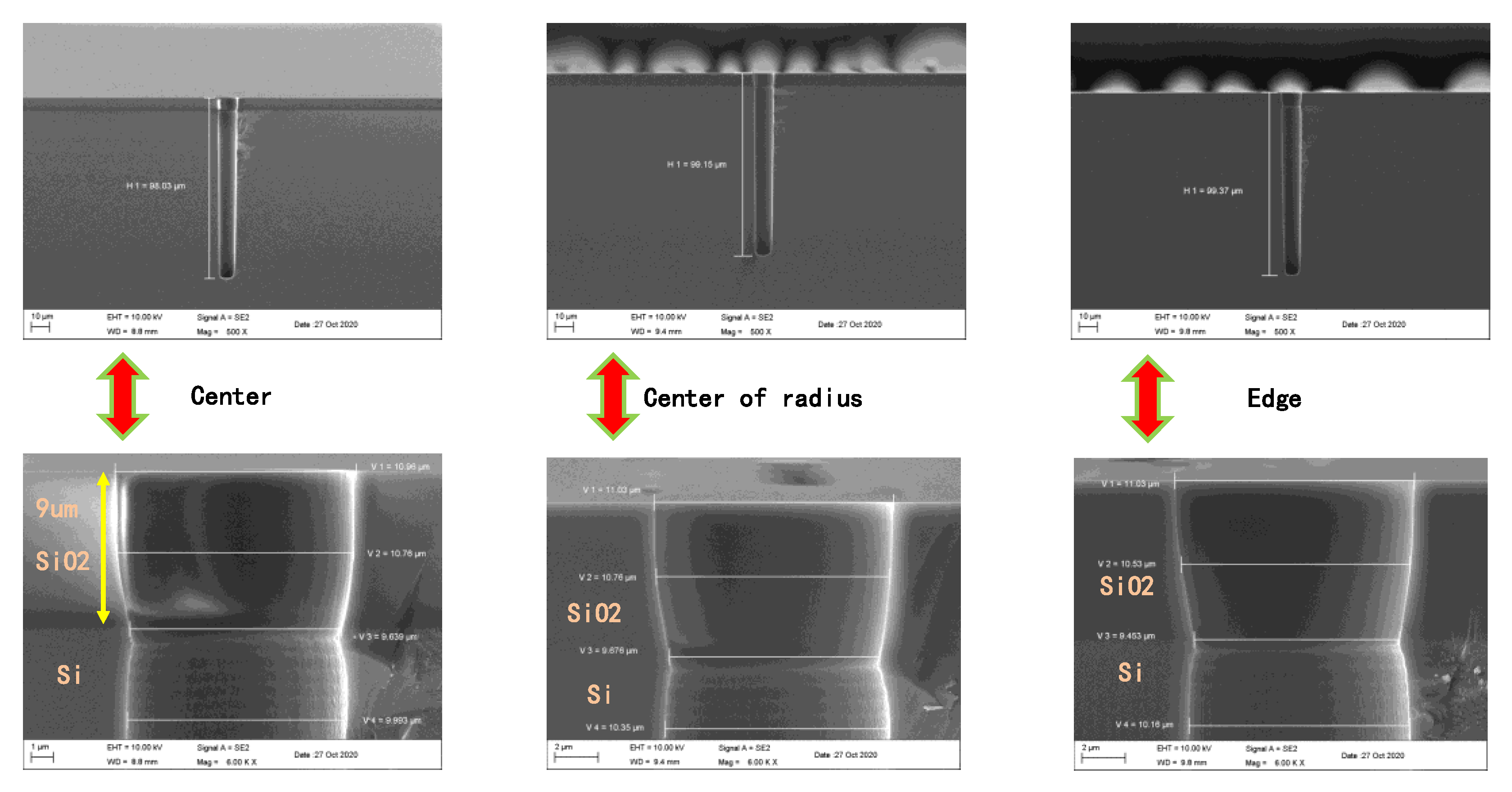
Furthermore, the plating filling of the TSV was performed and validated, as shown in
Figure 6. TSV sampling results at different locations show that copper is completely filled at all locations. The
thickness and TSV depth at different positions are shown in
Table 1.
At the same time, the etching process of edge coupler is verified. The side wall steepness of the ridge waveguide is optimized to achieve 80°. The release depth of silicon should be controlled within 25 um to prevent excessive dispensing after fiber coupling resulting in split. What is more, the spacing of the openings is reduced to prevent residual silicon from appearing under the BOX (buried oxide layer).
For the process diagram of EC first and TSV, the etching of the waveguide is first completed and then edge coupler etching and the release of silicon were conducted. The sealing process of the edge coupler needs to be performed to prevent the contamination of subsequent bonding. TSV process (etching, insulation and seed layer deposition and copper filling) and top RDL and UBM were conducted. The temporary bonding above is used to further make the outcrop of TSV and to complete the bottom RDL and copper pillar bumps (CPBS) on the backside.
Since SiO2 deposition is required to seal after EC process in order to prevent subsequent pollution, it will lead to the thickening of the
layer on Si, which highlights the problem of reliability and yield of TSV drilling process. In order to ensure the reliability of TSV process; the TSV first and then EC scheme was adopted to prepare the interposer. The stacking diagram of TSV preparation is shown in
Figure 7.
4. Package Substrate and Manufacture
The packaging substrate is designed with four layers and its size is 3.5 cm × 3.5 cm. Because it was not equipped with the actual signal transmission function, the design of high-speed interconnect was not carried out but some test structures were added. The detailed lamination design and material selection are shown in
Figure 8. SI10U(S) is the core material and PP 1078RC 54% is the interlayer dielectric material. The detailed electrical, thermal and mechanical properties of the materials are given in
Table 2.
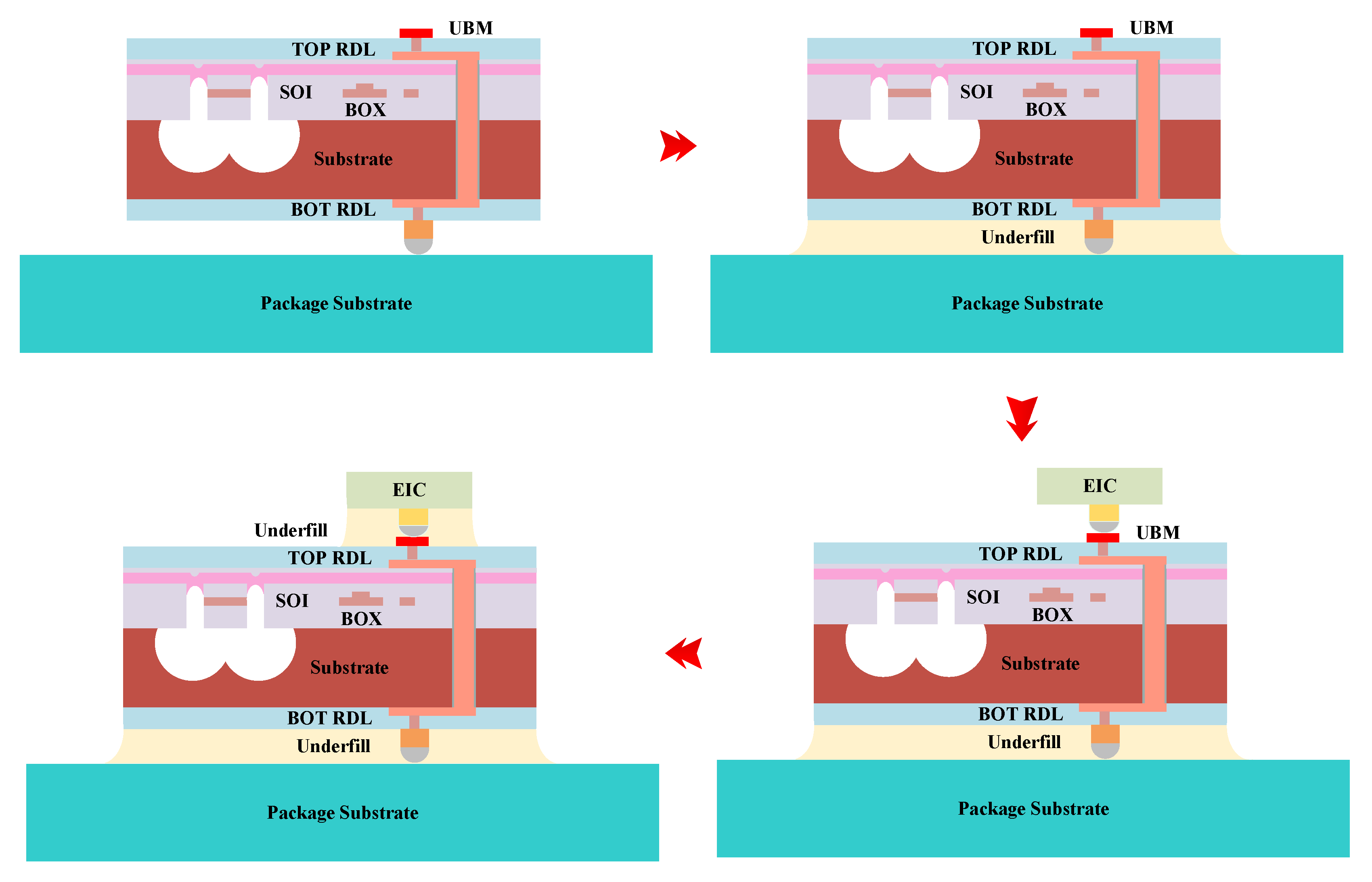
Figure 9 shows the assembly process of the 3D optical module. To avoid increasing the number of reflows, the active interposer is first mounted on the packaging substrate for reflow soldering and underfill filling and then the electrical chip is mounted on the adapter plate for reflow soldering and underfill filling. During underfill, excess glue entering the cavity of the edge coupler, causing breakage and reduced coupling performance, needs to be prevented. Therefore, it is necessary to avoid the position of the solder ball and the position of the edge coupler and fill the glue through the other side. The schematic diagram of cross-section of EIC on PIC on sub after assembly is shown in
Figure 10. The assembled 3D optical module is shown in
Figure 11. The detailed process and assembly flow is also shown in
Figure 11. In order to solve the problems of warpage and the influence of glue overflow on the edge coupler cavity in the three-dimensional assembly, underfill needs to be controlled to within 200 um of the chip and package substrate should preferably be controlled to above 1 mm.
5. Conclusions
Optical interconnection in data centers is becoming very important as the requirements for bandwidth, performance, power consumption and integration are further increasing. With the development of advanced packaging technology, the packaging schemes of optical chips and electrical chips have evolved from 2D to 2.5D and 3D. The application of active photonic interposer chips needs to solve the problem of the co-manufacturing of coupler and RDL-TSV-RDL interconnection structure and meet the requirements of high speed and low coupling loss.
Therefore, the fabrication of optical transceiver integrated with edge coupler and RDL-TSV-RDL and 3D assembly of modules were designed, validated and analyzed, and ideal high-frequency characteristics and extremely low optical coupling loss were achieved in this paper. Compatibility challenges for TSV and edge coupler manufacturing are validated and implemented. Different manufacturing processes were selected, validated and optimized to finally realize the active interposer manufacturing and 3D assembly.
This paper compares and selects different manufacturing solutions for active optical adapter boards and gives detailed design references for risk point parameters related to the assembly of 3D optical transceiver modules.
Author Contributions
Conceptualization, Q.Z. and H.X.; methodology, Q.Z. and H.H.; software, Q.Z. and F.D.; validation, H.X., F.L. and L.C.; formal analysis, F.L.; investigation, Q.Z.; resources, F.L., L.C. and P.S.; data curation, Q.Z.; writing—original draft preparation, Q.Z.; writing—review and editing, Q.Z. and H.X.; visualization, Q.Z..; supervision, Q.W.; project administration, H.X. and F.L. and L.C.; funding acquisition, F.L. and L.C. All authors have read and agreed to the published version of the manuscript.
Funding
This work was supported by the National Key Research and Development Program of China (No. 2022YFB2804403).
Data Availability Statement
The datasets generated during and/or analysis during the current study are available from the corresponding author on reasonable request.
Conflicts of Interest
The authors declare no conflict of interest.
References
- Minkenberg, C.; Krishnaswamy, R.; Zilkie, A.; Nelson, D. Co-packaged datacenter optics: Opportunities and challenges. IET Optoelectron. 2021, 15, 77–91. [Google Scholar] [CrossRef]
- Spyropoulou, M.; Kanakis, G.; Jiao, Y.; Stabile, R.; Calabretta, N.; Williams, K.; Avramopoulos, H. The path to 1Tb/s and beyond datacenter interconnect networks: Technologies, components, and subsystems. Metro Data Cent. Opt. Netw. Short-Reach. Links IV 2021, 11712, 73–81. [Google Scholar]
- Fathololoumi, S.; Hui, D.; Jadhav, S.; Chen, J.; Nguyen, K.; Sakib, M.N.; Liao, L. 1.6 Tbps silicon photonics integrated circuit and 800 Gbps photonic engine for switch co-packaging demonstration. J. Light. Technol. 2020, 39, 1155–1161. [Google Scholar] [CrossRef]
- Lorenz, L.; Hanesch, F.; Nieweglowski, K.; Hamjah, M.K.; Franke, J.; Hoffmann, G.A.; Bock, K. Reliability of 3D-Opto-MID Packages for Asymmetric Optical Bus Couplers. In Proceedings of the 2021 IEEE 71st Electronic Components and Technology Conference (ECTC), San Diego, CA, USA, 1–4 June 2021; IEEE: Piscataway, NY, USA, 2021; pp. 14–21. [Google Scholar]
- Abrams, N.C.; Cheng, Q.; Glick, M.; Jezzini, M.; Morrissey, P.; O’Brien, P.; Bergman, K. Silicon photonic 2.5 d multi-chip module transceiver for high-performance data centers. J. Light. Technol. 2020, 38, 3346–3357. [Google Scholar] [CrossRef]
- Li, M.; Wang, W.; Li, X. Simulation optimization of Wire bonding line matching based on FDTD algorithm. In Proceedings of the 2021 13th International Symposium on Antennas, Propagation and EM Theory (ISAPE), Zhuhai, China, 1–4 December 2021; IEEE: Piscataway, NY, USA, 2021; pp. 1–3. [Google Scholar]
- Guan, L.T.; Ching, E.W.L.; Ching, J.M.; Leng, L.W.; Wee, D.H.S.; Bhattacharya, S. FOWLP and Si-Interposer for High-Speed Photonic Packaging. In Proceedings of the 2021 IEEE 71st Electronic Components and Technology Conference (ECTC), San Diego, CA, USA, 1–4 June 2021; IEEE: Piscataway, NY, USA, 2021; pp. 250–255. [Google Scholar]
- Razdan, S.; de Dobbelaere, P.; Xue, J.; Prasad, A.; Patel, V. Advanced 2.5 D and 3D packaging technologies for next generation Silicon Photonics in high performance networking applications. In Proceedings of the 2022 IEEE 72nd Electronic Components and Technology Conference (ECTC), San Diego, CA, USA, 31 May–3 June 2022; IEEE: Piscataway, NY, USA, 2022; pp. 428–435. [Google Scholar]
- Zhang, W.; Ebert, M.; Reynolds, J.D.; Chen, B.; Yan, X.; Du, H.; Thomson, D.J. Buried 3D silicon photonics spot-size convertors. In Proceedings of the 2021 IEEE 17th International Conference on Group IV Photonics (GFP), Malaga, Spain, 7–10 December 2021; IEEE: Piscataway, NY, USA, 2021; pp. 1–2. [Google Scholar]
- Mu, X.; Wu, S.; Cheng, L.; Fu, H. Edge couplers in silicon photonic integrated circuits: A review. Appl. Sci. 2020, 10, 1538. [Google Scholar] [CrossRef]
- Cheng, L.; Mao, S.; Li, Z.; Han, Y.; Fu, H. Grating couplers on silicon photonics: Design principles, emerging trends and practical issues. Micromachines 2020, 11, 666. [Google Scholar] [CrossRef] [PubMed]
- Motoyoshi, M. Through-silicon via (TSV). Proc. IEEE 2009, 97, 43–48. [Google Scholar] [CrossRef]
- Yoon, S.W.; Yang, D.W.; Koo, J.H.; Padmanathan, M.; Carson, F. 3D TSV processes and its assembly/packaging technology. In Proceedings of the 2009 IEEE International Conference on 3D System Integration, San Francisco, CA, USA, 28–30 September 2009; IEEE: Piscataway, NY, USA, 2009; pp. 1–5. [Google Scholar]
- Wang, M.J.; Hung, C.Y.; Kao, C.L.; Lee, P.N.; Chen, C.H.; Hung, C.P.; Tong, H.M. TSV technology for 2.5 D IC solution. In Proceedings of the 2012 IEEE 62nd Electronic Components and Technology Conference, San Diego, CA, USA, 29 May–1 June 2012; IEEE: Piscataway, NY, USA, 2012; pp. 284–288. [Google Scholar]
- Papatryfonos, K.; Selviah, D.R.; Maman, A.; Hasharoni, K.; Brimont, A.; Zanzi, A.; Kraft, J.; Sidorov, V.; Seifried, M.; Baumgartner, Y.; et al. Co-package technology platform for low-power and low-cost data centers. Appl. Sci. 2021, 11, 6098. [Google Scholar] [CrossRef]
- Stone, R.; Chen, R.; Rahn, J.; Venkataraman, S.; Wang, X.; Schmidtke, K.; Stewart, J. Co-packaged optics for data center switching. In Proceedings of the 2020 European Conference on Optical Communications (ECOC), Brussels, Belgium, 6–10 December 2020; IEEE: Piscataway, NY, USA, 2020; pp. 1–3. [Google Scholar]
- Zheng, Q.; Yang, P.; Xue, H.; He, H.; Cao, R.; Dai, F.; Sun, P. Research on 3D Optical Module Integrating Edge Coupler and TSV. J. Light. Technol. 2022, 40, 6190–6200. [Google Scholar] [CrossRef]
- Traverso, M.; Mazzini, M.; Lakshmikumar, K.; Sunder, S.; Kurylak, A.; Appel, C.; Webster, M. Integrated silicon photonics transceiver module for 100Gbit/s 20km transmission. In Proceedings of the 2021 Optical Fiber Communications Conference and Exhibition (OFC), San Francisco, CA, USA, 6–10 June 2021; IEEE: Piscataway, NY, USA, 2021; pp. 1–3. [Google Scholar]
- Werner, S.; Navaridas, J.; Luján, M. A survey on optical network-on-chip architectures. ACM Computing Surveys (CSUR) 2017, 50, 1–37. [Google Scholar] [CrossRef]
- Ramirez, J.M.; Elfaiki, H.; Verolet, T.; Besancon, C.; Gallet, A.; Néel, D.; Achouche, M. III-V-on-silicon integration: From hybrid devices to heterogeneous photonic integrated circuits. IEEE J. Sel. Top. Quantum Electron. 2019, 26, 1–13. [Google Scholar] [CrossRef]
- Pares, G.; Bresson, N.; Moreau, S.; Lapras, V.; Henry, D.; Sillon, N. Effects of stress in polysilicon via-first TSV technology. In Proceedings of the 2010 12th Electronics Packaging Technology Conference, Singapore, 8–10 December 2010; IEEE: Piscataway, NY, USA, 2010; pp. 333–337. [Google Scholar]
- Liu, X.; Sun, Q.; Huang, Y.; Chen, Z.; Liu, G.; Zhang, D.W. Optimization of TSV leakage in via-middle tsv process for wafer-level packaging. Electronics 2021, 10, 2370. [Google Scholar] [CrossRef]
- Hicks, J.O.; Malta, D.; Bordelon, D.; Richter, D.; Hong, J.; Grindlay, J.; Allen, B.; Violette, D.P. TSV-last integration to replace ASIC wire bonds in the assembly of x-ray detector arrays. In Proceedings of the 2021 IEEE 71st Electronic Components and Technology Conference (ECTC), San Diego, CA, USA, 1 June–4 July 2021; IEEE: Piscataway, NY, USA, 2021; pp. 170–177. [Google Scholar]
- Chong, G.; Tan, C. Low temperature PE-TEOS oxide bonding assisted by a thin layer of high-κ dielectric. Electrochem. Solid-State Lett. 2009, 12, H408. [Google Scholar] [CrossRef]
| Publisher’s Note: MDPI stays neutral with regard to jurisdictional claims in published maps and institutional affiliations. |
© 2022 by the authors. Licensee MDPI, Basel, Switzerland. This article is an open access article distributed under the terms and conditions of the Creative Commons Attribution (CC BY) license (https://creativecommons.org/licenses/by/4.0/).


 ,
, 


